一种低开销的三节点翻转容忍锁存器设计
2024-06-21秦学伟
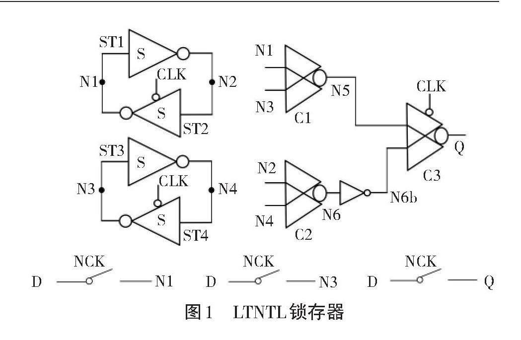
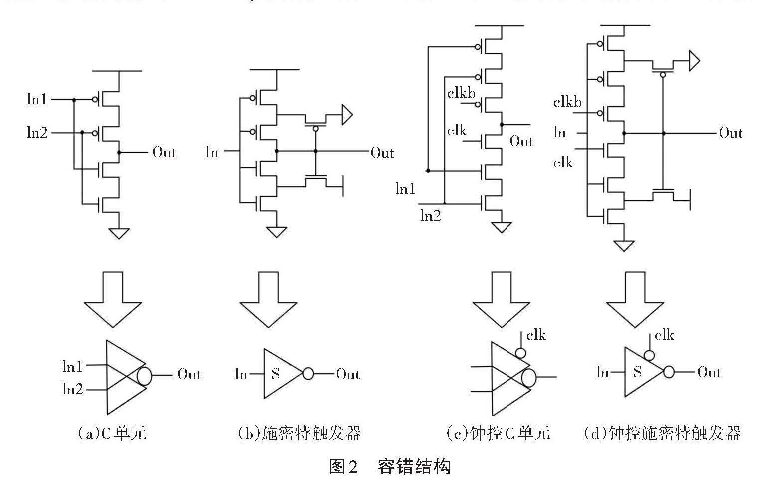

摘 要:【目的】随着半导体技术的发展,集成电路特征尺寸不断缩小,导致其对软错误更加敏感,因此需要对集成电路存储单元进行加固。【方法】使用Hspice进行实验与仿真,基于PTM32nm CMOS工艺,提出了一种低开销的三节点翻转容忍锁存器结构。【结果】该锁存器包含2个单节点自恢复模块、1个二级错误拦截模块、3个传输门。每个自恢复模块由1个施密特触发器和1个钟控的施密特触发器组成,首尾相连形成环形结构,有效地实现了三节点翻转的容忍。【结论】仿真结果表明:与现有的其他功能相同的锁存器相比,所提出的锁存器具有完整的三节点容忍能力,并且将功耗、延迟、面积、功率延迟积分别降低了约37.58%、41.25%、27.77%、75.83%。
关键词:锁存器;软错误;三节点翻转
中图分类号:TN47 文献标志码:A 文章编号:1003-5168(2024)08-0009-05
DOI:10.19968/j.cnki.hnkj.1003-5168.2024.08.002
Design of a Low-Cost Triple-Node-Upsettolerant Latch
QIN Xuewei
(School of Computer Science and Engineering, Anhui University of Science and Technology, Huainan 232001, China)
Abstract: [Purposes] With the development of semiconductor technology, the shrinking feature size of integrated circuits has made them more sensitive to soft errors, necessitating reinforcement of the storage units in integrated circuits. [Methods] Experiments and simulations were conducted using Hspice. Based on the PTM32nm CMOS process, a low-cost triple node upsets tolerant latch (LTNTL) structure was proposed. [Findings] The latch consists of 2 single-node self-recovery modules, 1 secondary error interception module, and 3 transmission gates. Each self-recovery module consists of a Schmitt trigger and a clock-gating Schmitt trigger connected in a loop structure, effectively achieving tolerance to TNU. [Conclusions] Simulation results demonstrate that compared to other latches with same functions, the proposed latch has complete TNU tolerance capability and reduces power consumption, delay, area, and power-delay product by approximately 37.58%, 41.25%, 27.77%, and 75.83%, respectively.
Keywords: latch; soft errors; triple node upset
0 引言
自从半导体技术进入纳米时代以来,晶体管的尺寸显著减小,导致电路节点的临界电荷也显著减少。集成电路(IC)越来越容易受到高能辐射影响而发生错误[1]。当辐射环境中的中子、质子、α粒子、γ射线等高能粒子撞击电路的敏感区域时,在库伦作用下,会有电子空穴对沿着高能粒子的运动轨迹产生[2]。晶体管的漏极会收集这些产生的电荷,当收集到的电荷超过临界电荷时,电路的逻辑状态可能会发生变化,从而导致单节点翻转(SNU)的发生。近年来由于集成电路尺寸的进一步缩小,产生的电荷共享效应使双节点(DNU)和三节点(TNU)翻转也变得更普遍[3]。而锁存器是集成电路中最常用的时序结构,硬化锁存器以容忍这些错误已成为一个重要的课题。……