Characteristic studies on positive and negative streamers of double-sided pulsed surface dielectric barrier discharge
2022-05-05YanJIANG姜岩BangfaPENG彭邦发ZhengyanLIU刘政妍NanJIANG姜楠NaLU鲁娜KefengSHANG商克峰andJieLI李杰
Yan JIANG (姜岩), Bangfa PENG (彭邦发), Zhengyan LIU (刘政妍),Nan JIANG (姜楠), Na LU (鲁娜), Kefeng SHANG (商克峰)and Jie LI (李杰),∗
1 School of Electrical Engineering,Dalian University of Technology,Dalian 116024,People’s Republic of China
2 School of Environmental Science & Technology, Dalian University of Technology, Dalian 116024,People’s Republic of China
Abstract The mechanisms of streamer generation and propagation in double-sided pulsed surface dielectric barrier discharge (SDBD)on both sides have been analyzed and investigated by experiment and numerical simulation.The fully exposed asymmetric SDBD has two discharge processes located on the high voltage electrode (HVE)side and the ground electrode(GE)side.Discharge images of the HVE side and GE side are taken by a digital camera under continuous pulse and ICCD (Intensified Charge Coupled Device)is utilized to diagnose the generation and propagation of streamers in single pulse discharge.In order to understand the physical mechanisms of streamer evolution more deeply,we establish a 2D simulation model and analyze it from the aspects of electron density, ion density, reduced electric field and electron impact ionization source term.The results show that the primary and secondary discharges on the HVE side and the GE side of the double-sided SDBD are composed of positive streamer and negative streamer, respectively.On the HVE side, the accumulation of positive charges on the dielectric surface causes the direction of the electric field to reverse, which is the principal factor for the polarity reversal of the streamer.On the GE side,both the negative charges accumulated on the dielectric surface and the falling voltage are the key factors for the streamer polarity switch.
Keywords: double-sided SDBD, positive streamer, negative streamer, nanosecond pulse
1.Introduction
Surface dielectric barrier discharge(SDBD)is a common form of discharge to generate non-thermal plasma extending along the dielectric surface,which uses the dielectric layer to separate two metal electrodes to prevent the discharge from turning into sparks or arcs.It has attracted enormous research interest in gas treatment or flow control due to its simple structure and low flow resistance[1-3].In recent years,some researchers also put forward the use of SDBD for anti-icing and de-icing application, which is considered a promising method [4-7].
While the application field of SDBD is expanding,people are further studying its discharge mechanisms.Peng et al studied the phenomena of primary and secondary streamers in the discharge process of traditional two-electrode nanosecond pulse SDBD[8].When a second GE was arranged on the HVE side, a transitional streamer stage was found, which occurred between the primary streamer stage and secondary streamer stage [9].Lei et al obtained the energy curve of the two discharge processes by the circuit model of nanosecond pulse SDBD discharge [10].Zhu et al studied the development process of streamer in the process of nanosecond pulse SDBD by means of numerical simulation and experiment [11], and obtained the energy distribution curve during discharge by coupling fluid model, photoionization model and Euler equation [12].Their further research demonstrated that secondary ionization waves occurred at the edge of the HVE during streamer extension[13].In addition,the surface charge sensors [14, 15], dielectric temperature [16] and optical emission spectroscopy[17] are also utilized to provide insight into the discharge characteristics and discharge process of SDBD.
However, the above studies on discharge plasma in encapsulated SDBD [18, 19] were restricted to one side of the dielectric where the plasma ignites from only the single-phase electrode, that is, either cathode or anode.In fact, the plasma generated only on one side of the dielectric limits the extension of the plasma area, and prevents the efficiency of the SDBD plasma actuator from being wholly utilized in practical applications.Nevertheless,exposing the GE to produce the double-sided discharge of the dielectric can not only expand the discharge area,but can also generate more active particles and heat without increasing the number of electrodes.This also means that doublesided SDBD will be an efficient and promising method in gas purification [20], de-icing [21], conversion of organic compounds [22] and catalyst-enhanced plasma oxidation [23].Meanwhile,the inherent mechanisms behind the evolution of the plasma discharge in double-sided SDBD are still not thoroughly understood.It denotes that we lack substantial knowledge and essential research for the discharge of such configurations.
Therefore,the plasma propagation process of asymmetric double-sided SDBD is investigated in the present work.The research of this paper is primarily composed of the experimental part in section 3.1 and the simulation part in section 3.2.In section 3.1, the discharge morphology and power of double-sided SDBD under continuous pulse discharge at different rising times are firstly explored, and then the positive and negative streamer process of double-sided SDBD under single pulse discharge is studied by ICCD camera.In section 3.2, we computationally investigate the underlying mechanisms of streamer formation and behavior in double-sided SDBD through species generation and distribution in the discharge domain and dielectric surface.
2.Experimental setup and numerical modeling
2.1.Experimental setup
The experimental system diagram and geometric structure diagram are shown in figure 1.The dielectric is Kapton film with a thickness of 0.25 mm, and the electrode material is 0.08 mm aluminum foil.The width and length of HVE and GE are both 10 mm and 60 mm,and the overlap gap is 1 mm.The power supply is a positive high voltage nanosecond pulse supply (HVP-20P, Xi’an Smart Maple Electronic Technology Co.Ltd,China.Rise time and drop time of pulse range from 50 to 500 ns, pulse amplitude ranges from 0 to 20 kV).Under continuous pulse discharge, the images are captured by a digital camera(Canon 700D,canonEF-M28M MF3.5 IS STM lens),the aperture is set as 2.8,the exposure time is 0.04 s,and the sensitivity is 12800.During the discharge process,5 V TTL signal from the nanosecond pulse power supply is used to trigger ICCD camera (Princeton, Pi-Max 3 1024I, minimum gate width 2.87 ns, with Canon 50 mm F/1.8 lens)to obtain the evolution and propagation of streamers.In the experiment,a voltage probe (Tektronix P6015A)and a current probe(Tektronix P6021)are used to monitor the applied voltage and current.Both voltage and current waveforms are recorded by a digital phosphor oscilloscope (Tektronix DPO3012).
2.2.Numerical modeling
2.2.1.The governing equation.In order to further disclose the development and propagation mechanisms of doublesided SDBD streamers along the dielectric surface,COMSOL Multiphysics built-in plasma module is used for simulation analysis.The module coupled the particle continuity equation,the electron energy conservation equation, and the Poisson equation describing the electric potential.Where the continuity equation is as follows:

In formula (1),tis time,niis the number density of neutral particles,ions and electrons,iμis the migration coefficient of electrons and ions, and E is the vector electric field.Siis the chemical source term, representing the change of particleiobtained through the reaction of generation and consumption,which can be obtained by the following formula:

Whereci,rrepresents the stoichiometric coefficient of particle i in reactionr, andRi,rrepresents the reaction rate.
As an important parameter in the study of lowtemperature plasma, the change of electron energy can be used to describe the plasma discharge process, and the expression is as follows:

Herenεis the electron energy density;μεrepresents the electron energy transfer coefficient;Dεis the diffusion coefficient of electron energy;Sεrepresents the chemical source term of electron energy, expressed as follows:

-e(μene·E-De∇ne)·Eis the Joule heat of an electron in an electric field,is the change in electron energy due to a chemical reaction, andrepresents the energy transfer of an electron in reaction r.
In SDBD, the dielectric surface charge and space charge have a significant influence, and the change of electric field caused by the dielectric surface charge and space charge in the discharge process can be obtained by solving the Poisson equation:

Where,0εis the vacuum permittivity,εris the relative permittivity of materials, andqρis the space charge density.
The rate coefficient of electron collision reaction can be obtained by the following formula:
In the computation process, Einstein’s relation is as follows:
The electron diffusion coefficientDe,electron energy migration coefficientμεand electron energy diffusion coefficientDεcan be obtained by the above formula.Where,μeis the elect ron energy mobility coefficient, which is consistent with the reduced electron mobilityμεNnin [26],whereNnis the density of neutral particles;Tεis the electronic temperature,which can be obtained by the following formula,andkBis Boltzmann constant:

Diffusion coefficients of ion and neutral particles can be obtained by the following formula:

In the formula,iωis the mass fraction of particlesi;xjis the mole fraction of the particlej;Dijis the binary diffusion coefficient of particleiand particlej.
The ion mobility is as follows,where the gas temperature isTg:

2.2.2.Initial values and boundary conditions.Reasonable boundary conditions and initial values are necessary for effective numerical simulation [27].Since the discharge is carried out at atmospheric pressure,the gas temperature is set as 273.15 K and the pressure is set as 1 atm in the simulation.The gas heating in the discharge process is ignored.The initial electron density and charged particle density are both 1 × 10¹⁵m−3to maintain the initial electric neutrality of the gas.Considering the composition of air, the volume fraction of N2is set as 0.79, and O2satisfies the principle of mass constraint.The electron flux and electron energy flux at the outer boundary of the discharge area are 0,which satisfies the equations-n·Γe= 0and-n·Γε=0.Set the charge to be conserved in the dielectric region and able to accumulate on the dielectric surface, satisfying the following expression:

In the formula,sρis the surface charge density,n·Jiis the normal component of the total ion current density,n·Jeis the normal component of the total electron current density.
The secondary electron flux and the secondary electron energy flux on the dielectric surface and electrode surface are expressed by the following formula:

Here,ve,this the electron thermal velocity,neis the electron density, andpγis the secondary electron emission coefficient of the ionp.The nanosecond pulsed voltage waveform applied on the HVE in simulation comes from an oscilloscope in the experiment.
2.2.3.Computational domain.In order to reduce the consumption of computation resources and time, simplification of the calculation region is required, as shown in figure 2.Through pre-simulation and experiments, it is found that the upper and lower surface plasmas have different lengths, so the high voltage electrode and ground electrode must have a suitable range.Here,the width of the HVE is set as 5 mm,the width of the GE is 6 mm,and the overlap is 1 mm.The thickness of the electrode and the dielectric are 0.08 mm and 0.25 mm respectively.The whole computational domain is divided by triangular mesh,and the mesh refinement is carried out near the electrode and dielectric surface, where the particle density changes greatly and the reaction is more.
2.2.4.Chemical reaction model.Discharge in air is a complex process, which includes a series of chemical reactions(ionization, excitation, dissociation, recombination, attachment,quenching and charge transfer[8]).In this simulation model,61 dominated chemical reactions are considered, including 25 species, as listed in table 1.The SEEC (secondary electron emission coefficient)is set to 0.01 [35].
The maximum BDF (backward differentiation formula)order is set to 2 and the minimum BDF order is set to 1 for time integration.A parallel sparse direct solver(PARDISO)is chosen to solve the equations.Due to the highly nonlinear nature of the discharge and the refinement of the partial grid,the calculation consumes about 577 h by using a computer with a 3.07 GHz Intel(R)Xeon(R)processor in 64-bit mode running in 48 GB memory.
3.Results and analysis
3.1.Experimental results and analysis
3.1.1.Continuous pulse discharge image.In practical application, the steady working state of double-sided nanosecond pulse SDBD is supplied by continuously pulsed voltage.Therefore, researching discharge characteristics under this condition contributes to a preliminary understanding of the discharge process of such a structure.Figure 3 shows the variation of voltage and current waveform and discharge image with different pulse rising times as pulse voltage peak is 9 kV and pulse repetition frequency is 1000 Hz.From the discharge image in figure 3,we can see that the HVE presents the characteristics of bright discharge channel and apparent filaments positivepolarity streamer,while the GE side presents the characteristics of diffuse discharge channel and non-filament-like negative-polarity streamer.This also indicates that the discharges of the HVE side and the GE side have a great difference, and the specific discharge process needs to be further investigated.With the rise time increasing from 50 to 500 ns, the luminance of the HVE side and GE side gradually decreases, but the discharge uniformity and the number of filaments are on the rise.This is because the voltage rise rates du/dt decrease from 1.8 × 10⁸to 1.8 × 10⁷kV s−1leading to the degree of electric field distortion weakening, which denotes that the probability of electron collision and electron velocity is reduced.Correspondingly, the energy obtained by the electrons also cut back,as we can see the discharge power decrease in figure 4.The discharge power is calculated as followswhere f represents pulse repetition frequency, u(ε)and i(ε)represent voltage and current respectively.Meanwhile, the peak value of the positive current is decreasing,while the peak value of the negative current is basically unchanged.These phenomena indicate that there may be different discharge stages in the double-sided pulsed SDBD,and the variation of the pulse voltage rise time will only affect the discharge stage corresponding to the positive peak current.The discharge process will be further explored in the next section under single pulse power supply.

Figure 1.Experimental setup.(a)Experimental system diagram, (b)geometric structure diagram.

Figure 2.Numerical computation domain.

Figure 3.Voltage and current waveform and discharge image at different rising time.(a)HVE side, (b)GE side.

Figure 4.Variation of pulse discharge power of double-sided SDBD with rising time at different voltages.
3.1.2.Streamer evolution, primary streamer and secondary streamer under single pulse discharge.After studying thedischarge characteristics of the double-sided SDBD in a stable discharge state, an ICCD camera is used to acquire time-resolved images of the plasma evolution for analyzing the dynamics of the streamer along the surface on different sides.In the experiment, the pulse voltage rise time, pulse duration time, and fall time are all 50 ns, and the discharge voltage is 9 kV.As can be seen from the streamer evolution diagram in figure 5,the streamer development process of both the HVE side and the GE side has two stages, namely the positive streamer stage in primary discharge(primary positive streamer)and the negative streamer stage in secondary discharge (secondary negative streamer)on HVE side,negative streamer stage in primary discharge (primary negative streamer)and positive streamer stage in secondary discharge (secondary positive streamer)on GE side.
The purchase of the card each week is not done out of habit. It is my romantic mission each week to find the right card. At times, my search takes me to many different card stores to find that perfect offering. I have been known to spend a considerable amount of time in front of the card displays, reading up to a dozen different cards before I choose the right one. The picture and the words in the card must have specific meaning to me and must remind me in some way of Patricia and our life together. The card needs to evoke6 an emotion in me. I know that if a card brings a tear of happiness to my eyes, I have found the right one.

Table 1.The considered collision reactions in the model(Units for two-body reactions in cm3 s−1,three-body reactions in cm6 s−1,electron temperature Te in eV and gas temperature Tg in K).

Table 1.(Continued.)
Firstly, in the HVE side region in figure 5(a), from 5 to 65 ns, after applying a positive high-voltage pulse to the HVE, a forward electric field is formed from the HVE to the dielectric surface.With the further increase of the voltage,the forward electric field enhances, inducing the electrons avalanche, and then generating streamer propagating along the dielectric surface.As the streamer head moves forward,a large amount of positive charge accumulates on the dielectric surface,thus weakening the positive electric field between the HVE and the dielectric surface.As a result, the luminous intensity of the streamer changes from weak to strong,then to weak until it disappears.It is worth noting that at 25 ns in figure 5(a), before the extended streamer disappears, we can observe that re-generation of discharge occurs at the edge of the HVE.This is because the streamer channel during the streamer propagation process cannot shield the increasing external electric field, and there remains a highly pre-ionized plasma near the electrode left by the streamer head, which causes the discharge to occur again.This discharge process is called the secondary ionization wave [13], which has the same polarity as the streamer head passed by in the streamer channel.Therefore, the primary positive streamer consists of the luminous streamer head and the secondary ionization wave.From 135 to 195 ns, in the process of pulse voltage drop, the polarity of the electric field between the HVE and the dielectric surface is reversed.At this time, the dielectric surface acts as a virtual anode and the metal electrode acts as a cathode.Further reduction of the supply voltage strengthens the reverse electric field, and a large number of electrons move towards the dielectric surface, forming a secondary negative streamer that propagates along the dielectric surface.The extended secondary negative streamer makes the positive charge accumulated on the dielectric surface be neutralized and consumed continuously which weakens the reverse electric field, and the secondary negative streamer process on the HVE side comes to an end.
Secondly, in figure 5(b), we can see that the primary negative streamer and the secondary positive streamer on the GE side have remained near the vicinity of the electrode,and there is no detached streamer head moving in the streamer channel like the HVE side.In the primary negative streamer process, from 5 to 35 ns, electrons move towards the dielectric surface and cause ionization through electron collision, so the number of electrons and ions increases exponentially.Therefore, the luminescence intensity of the primary negative streamer on the GE side increases continuously, meanwhile, the coverage area of plasma also extends.Nonetheless, with the accumulation of negative charge on the dielectric surface, the original electric field weakens, causing the luminous intensity of the streamer to gradually decrease from 45 to 65 ns.Thereafter, a large number of negative charges accumulated on the dielectric surface reverse the direction of the electric field,resulting in a secondary positive streamer process.From 135 to 195 ns, it can be seen that the discharge in this process is considerably feeble, and both the luminous intensity and the propagation distance are far inferior to the primary negative streamer process.
By adjusting the ICCD gate width time according to the streamer evolution process in figure 5, complete primary streamer images, secondary streamer images and the whole streamer images on the HVE side and GE side are displayed in figure 6.Corresponding to the voltage and current waveform acquired in the discharge process, we found that the primary streamer occurs in the rising stage and the initial falling stage of the pulse voltage, and the secondary streamer occurs in the falling stage of the pulse voltage.In addition,discharge current in the primary streamer stage is positive,whereas in the secondary streamer stage is negative.This is consistent with the results obtained by Peng et al [8] in the study of streamer development mechanisms in encapsulated SDBD.
Figure 7 is the cross-section distribution of the average luminous intensity of streamers.It can be seen that the primary streamer has a stronger luminous intensity and a longer propagation distance than the secondary streamer regardless of on the HVE side or GE side.Particularly,primary negative streamers have a higher streamer intensity than primary positive streamers,by about a factor of two.It is shown that the charge accumulated on the dielectric surface is less after the primary streamer passes through, hence the secondary streamer has a shorter propagation distance and weaker luminous intensity.

Figure 5.Evolution diagram of streamer development process.(a)HVE side, (b)GE side.

Figure 6.Waveform of voltage and current and morphology of primary and secondary streamers.(a)HVE side, (b)GE side.

Figure 7.Cross-section distribution of streamer luminescence intensity on dielectric surface.

Figure 8.Spatial evolution of electron density.

Figure 9.Spatial evolution of positive ion density.
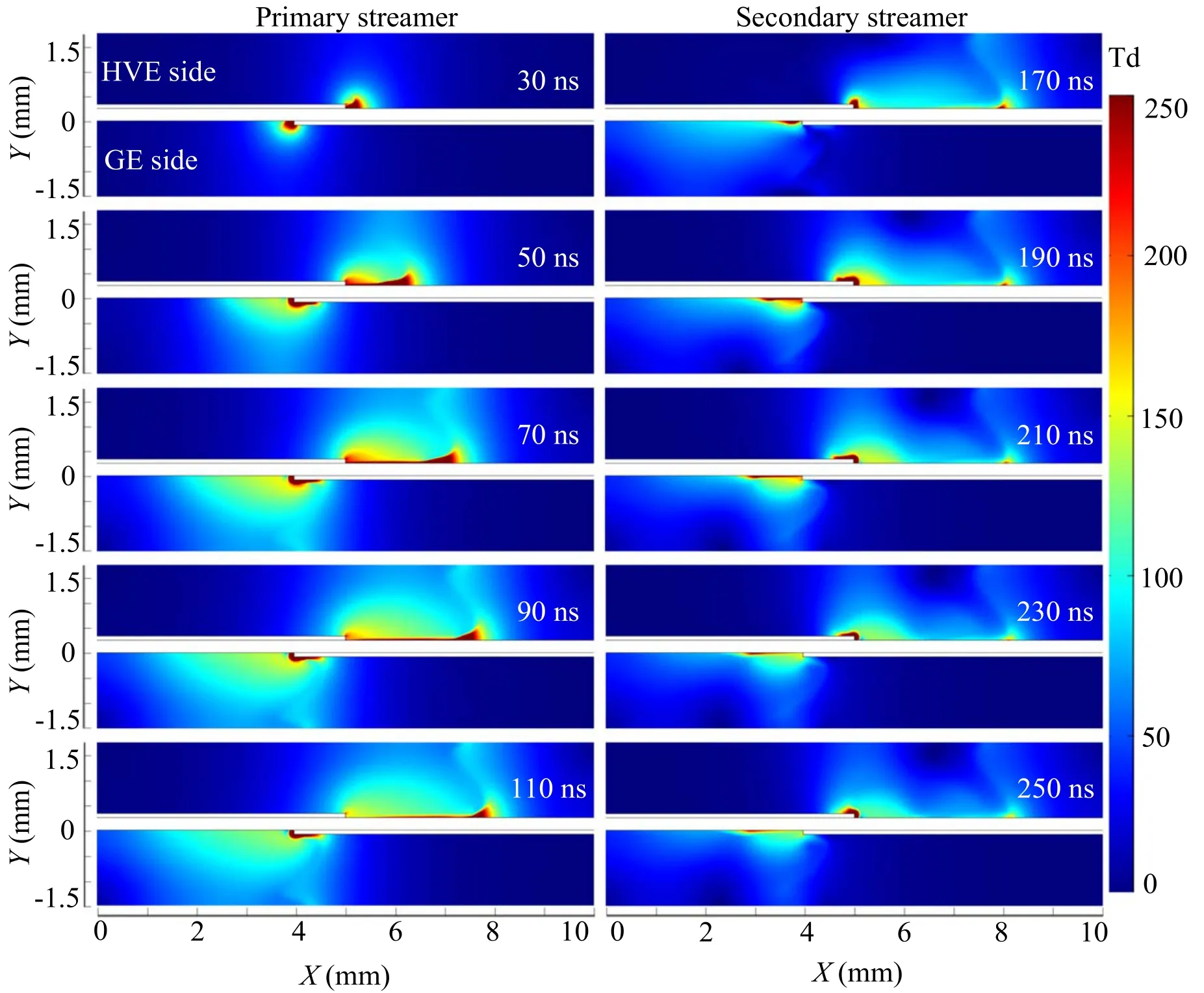
Figure 10.Evolution process of spatially reduced electric field.

Figure 11.Evolution process of electron collision ionization source term.

Figure 12.Calculated electrical characteristic.

Figure 13.Variation of dielectric surface charge during primary and secondary streamers.(a)GE side, (b)HVE side.
3.2.Numerical simulation results and analysis
In the experimental results and analysis in the previous section, it is uncovered that primary and secondary streamers occur on both the HVE and the GE side.In addition,a partial explanation is provided for the generation and propagation of streamers.In this section, we will further explore the entire streamer initiation and propagation process of double-sided SDBD through numerical simulation and give a more detailed explanation.The electron density distribution, positive ion density distribution, i.e., summation of O+,N2+and O2+ions,and reduced electric field and electron collision ionization source term are shown in figures 8-11, respectively.
3.2.1.Evolution process of streamer on the HVE side.In figure 8, as positively pulsed voltage is implemented to the HVE, the seed electrons uniformly distributed in space migrate to the HVE, resulting in extremely high electron density at the HVE.At 30 ns, it can be observed that the primary positive streamer initiates in the local proximity of HVE.The accelerated electrons in the electric field collide with the background gas, causing the electron avalanche and the extension of the primary positive streamer.As the mobility of positive ions is much lower than that of electrons, positive ions are left in the streamer head.Under the effect of electric field force, positive ions move towards the dielectric surface and form a cathode sheath layer between the dielectric surface and plasma.This can be proved by the distribution and evolution diagram of positive ions in figure 9.In figure 8, during the primary positive streamer process, the existence of the cathode sheath layer makes a gap of dozens of microns between the streamer and the dielectric surface,and the gap is the largest at the streamer head.With the streamer propagating continuously, the gap between the streamer head and the dielectric surface keeps shrinking.In figure 10, from 30 to 110 ns, we can see that the floating streamer head and the cathode sheath layer located on dielectric surface always have the highest reduced field strength.The reason for this phenomenon is that the positive ions further strengthen the electric field between streamer and dielectric surface when they are close to the dielectric surface,and the corresponding electron impact ionization reaction takes place in cathode sheath layer and streamer head.This also proves that the propagation of the primary positive streamer on the HVE side mainly depends on the strong ionization reaction at the floating streamer head.Between 30 and 110 ns, with the continuous expansion of volume and propagation distance of streamer, the electron density in figure 8,the reduced electric field in figure 10 and the electron collision ionization reaction in figure 11 show a trend of increasing first and then decreasing, while the positive ion density in figure 10 shows a trend of increasing first and then unchanged.This indicates that the reverse electric field generated by the positive ions accumulated on the dielectric surface begins to counteract the forward electric field generated from HVE, resulting in the decrease of electron density, the corresponding reduction of the reduced electric field, and the reduction of ionization reaction of electron collision.As the power supply voltage decreases,the intensity of the reverse electric field is greater than that of the forward electric field.It means that the polarity of the electric field reverses and discharge enters the secondary negative streamer stage.
Between 170 and 250 ns, electrons no longer move towards the metal electrode but towards the dielectric surface,which acts as a virtual anode.In figure 8,the location close to the metal electrode has higher electric field intensity,thus it can be seen that the secondary negative streamer ignites on the dielectric surface several hundred microns away from the metal cathode and then moves towards the metallic cathode at 170 ns.From figure 9, we can see that the streamer head oriented toward the metal cathode gathers a large number of positive ions.After reaching the metal cathode,the positive ions adhere to the metal cathode to form a cathode sheath layer at 210 ns and extend within a small range, which is consistent with the results obtained by Nguyen-Smith et al [36].In figure 10, as the positive ions further enhance the electric field between the streamer and the metal cathode in the process of approaching the metal cathode, the high reduced electric field is primarily concentrated at the cathode sheath layer.The cathode sheath layer composed of positive ions attracts a large number of electrons around the sheath, causing new electron collision ionization reactions and enlarging the coverage of streamers in the X-axis and Y-axis.In the secondary negative streamer process,we can see from figures 9-11 that positive ion density,reduced electric field and electron collision ionization source term all show a trend of gradually increasing at first and then decreasing.The main reason is that the electrons constantly move to the dielectric surface and neutralize the positive charge on the dielectric surface, which weakens the reverse electric field and inhibits the discharge from continuing.However, in figures 10 and 11,we can still see that the electron cannot reach the dielectric surface 3 mm away from the HVE due to the weak electric field.It can explain why the residual positive charge of the primary positive streamer far away from the HVE can exist for a long time.
3.2.2.Evolution process of streamer on the GE side.During the process of primary negative streamer from 30 to 110 ns,the barrier dielectric beneath the HVE is polarized upon the application of an electric field.The closer to the GE,the greater the intensity of the electric field and the higher the degree of polarization of the barrier dielectric is.The maximum value of the surface potential of the dielectric is equal to the value of the applied pulse voltage.Consequently, the surface potential of the barrier dielectric appears as a positive potential and changes synchronously with the pulse voltage before negative charges begin to accumulate on the dielectric surface.A forward electric field is generated from the dielectric surface to the metallic cathode.Under these conditions the electron avalanche directed toward the anodic dielectric surface initiates the discharge.In essence, the ignition position of the streamer should be located where the electric field is highest, and it would be expected that the primary negative streamer would take place at the intersection of the GE and dielectric surface.However,at this point,electrons do not have enough space to obtain sufficient energy for ionization [36].Therefore, after multiple executions of the simulation, it can be seen that initially the primary negative streamer is ignited at a distance of about 200 μm away from the GE in figure 8.Subsequently,the positive ions concentrated on the right-hand side of the streamer bulk move towards the metallic cathode until they adhere to the GE and form a cathode sheath layer at 50 ns as illustrated in figure 9.We can see that the cathode sheath layer with a highly reduced electric field is mainly composed of positive ions, attracting a partial number of electrons for ionization, and promoting the propagation of streamers.Additionally, the electrons and negative ions move to the dielectric surface and are collected, then they repel each other after reaching the dielectric surface, causing the primary negative streamer to further enlarge in the X-axis and Y-axis directions.Different from the strong ionization reaction at the positively charged streamer head which leads the primary positive streamer to propagate on the HVE side, the primary negative streamer on the GE side relies on the movement of electrons and anions towards the dielectric surface.
With the accumulation of negative charges on the dielectric surface and the reduction of the pulse voltage, the polarity of the electric field switches and the dielectric surface takes on the role of a virtual cathode.In figure 8, it can be seen that the secondary positive streamer initiates near the intersection of the GE and dielectric surface, and then it propagates into both negative the X- and Y-directions.In figures 9 and 11,the propagation process similar to that of the primary positive streamer on the HVE side can be observed from 190 to 250 ns.That is to say,the positive streamer head with a strong ionization reaction dominates the streamer propagation.Meanwhile, the cathode sheath with high reduced electric field forms between streamer bulk and dielectric surface.
3.2.3.Surface charge and surface potential of the dielectric.As seen from figure 13(a),the amount of charge accumulated on the dielectric surface depends considerably on the distance from the electrode.Essentially,the farther away from the GE,the surface charge is accumulated more slowly.Accordingly,quantities of negative charges accumulate at a position 0.2 mm away from the GE, and there is virtually no accumulation of negative charges at 3.8 mm away from the GE.As for this situation, the main reason is that the electric field reduces proportional to the square of the distance from the electrode, such that electrons and negative ions are no longer able to arrive any further [36].Once the primary discharge has been ignited, the dielectric surface acts as a virtual anode attracting massive electrons and negative ions to it as the primary negative streamer propagates along the dielectric surface.Consequently, the negative charges of the whole dielectric surface increase swiftly and reach the maximum value at 100 ns.As the voltage declines, the reverse electric field generated by negative charges of dielectric surface is greater than the forward electric field causing the secondary discharge to occur at 170 ns.Due to polarity switch,the electric field is reversed,thus electrons are pushed away from the dielectric surface.The cathodeoriented positively charged streamer head promotes the propagation distance of secondary positive streamers, such that a portion of negative charges of dielectric surface are neutralized.During this process, the reduction of negative charges,in turn,weakens the reverse electric field.Therefore,the secondary positive streamer has a smaller propagation length compared to the primary negative streamer.It should be noted that the residual surface charge is not readily removed or dissipated due to the limited length of the secondary positive streamer, such that residual charge can be detected on the surface after several hours and even days[15].
In figure 13(b), we can see the dynamics distribution of surface charges on the HVE side.Similarly, as the primary positive streamer propagates continuously along the dielectric surface, the coverage distance of the positive surface charge on the dielectric surface increases, up to 2.8 mm from the electrode.Note that the largest surface charge accumulation occurs at the edge of the metallic electrode.At 170 ns, the secondary discharge takes place in reverse electric field and dielectric surface takes on the role of virtual anode.Subsequently, electrons and negative ions in the secondary negative streamer are pushed toward the dielectric surface leading to the dissipation of positive surface charge.Likewise, on the HVE side, primary positive streamers have longer propagation distance than secondary negative streamers, by about a factor of two.These results are in good agreement with the experimental results.
Figure 14 is a cross-sectional distribution diagram of the dielectric surface potential at different discharge times on the HVE side and the GE side.In figure 14(b),we can see that the surface potential is exclusively determined by the accumulated charge on the dielectric surface.Thus,the variation curve of the dielectric surface potential is completely consistent with the variation trend of the dielectric surface charge.Nevertheless,the surface potential on the GE side is determined by both the negative charge accumulated on the dielectric surface and the applied pulse voltage.In figure 14(a), the dielectric surface potential is equivalent to the pulse voltage due to the dielectric surface being polarized before primary negative streamers have formed.The disparity of the surface potential located at different positions on the dielectric surface appears and further increases with the extension of negative streamers.At 160 ns,we can see that the surface potentials of +5.6 kV and −0.4 kV simultaneously exist on the dielectric surface.That is to say,the applied voltage and negative charges of the dielectric surface work together to promote the generation of secondary positive streamers.At 210 ns, namely after the applied voltage drops to 0,the dielectric surface always presents negative potential due to the existence of residual negative charge.Figure 15 is the evolution of spatial electric field vector distribution in different discharge periods.We can see that the source term of the excited electric field changes constantly, which corresponds to the development and propagation of streamers and the accumulation of charge on the dielectric surface.

Figure 14.Variation of dielectric surface potential during primary and secondary streamers.(a)GE side, (b)HVE side.

Figure 15.Evolution of spatial electric field vector distribution.
4.Conclusions
In this work,the studies of streamer evolution of double-sided asymmetric structure SDBD are carried out via experiment and numerical simulation.The main characteristics can be obtained as follows:
(1)From the images of continuous pulses discharge, it has been identified that the discharge presents a filamentlike positive streamer on the HVE side and diffuse negative streamer on the GE side, respectively.In addition, the discharge power of double-sided SDBD decreases with the increase in rise time.From ICCD,the streamer development process of both the HVE side and the GE side has two stages, namely primary positive streamer and secondary negative streamer on the HVE side,primary negative streamer and secondary positive streamer on GE side.
(2)For streamers on the HVE side,the streamer process on the HVE side consists of primary positive streamers and secondary negative streamers.The propagation of the primary positive streamer is dominated by the ionization reaction at the streamer head,corresponding to the bright streamer head seen in the experiment.The positive charge on the dielectric surface progressively accumulates with the extension of the primary positive streamer causing the surface potential of the dielectric to increase until the reverse electric field is generated.Subsequently, the secondary negative streamer is ignited from the dielectric surface close to the metal electrode.The dielectric surface acting as a virtual anode attracts a large number of electrons at the same time, expanding the streamer until the positive charge near the metallic electrode dissipates,and the secondary negative streamer process ends.It should be noted that the positive charges accumulated on the dielectric surface are the principal factor for the polarity reversal of the streamer on the HVE side.
(3)However, the streamer evolution on the GE side is different from the HV side.The whole streamer process on the GE side consists of the primary negative streamer and the secondary positive streamer.During the primary negative streamer process, the barrier dielectric is polarized by a pulsed voltage into a virtual anode.Therefore, we can see the primary negative streamer ignited at a distance of 200 μm from the GE.With the accumulation of negative charges on the dielectric surface far away from the GE, the reverse electric field appears and weakens the original electric field until the end of the primary negative streamer process.Due to the accumulation of negative charge and polarization of the pulse voltage, both positive and negative potentials appear on the dielectric surface on the GE side, and work together to promote the generation of the secondary positive streamer.After the pulsed voltage drops to 0, the whole dielectric surface presents negative potential because of the existence of residual negative charge.
Acknowledgments
This work is supported by National Natural Science Foundation of China (Nos.51877027 and 52107140)and Project funded by China Postdoctoral Science Foundation (No.2021M700662).
ORCID iDs
猜你喜欢
杂志排行

Plasma Science and Technology的其它文章
- Numerical analysis on the effect of process parameters on deposition geometry in wire arc additive manufacturing
- Investigation of the gas bubble dynamics induced by an electric arc in insulation oil
- The influence of charge characteristics of suspension droplets on the ion flow field in different temperatures and humidity
- Hydrophobicity changes of polluted silicone rubber introduced by spatial and dose distribution of plasma jet
- Characteristics of water volatilization and oxides generation by using positive and negative corona
- Preparation of N-doped graphite oxide for supercapacitors by NH3 cold plasma