沟道长度对IGZO薄膜晶体管性能的影响
2021-10-18刘璐高晓红孟冰付钰孙玉轩王森刘羽飞胡顶旺
刘璐 高晓红 孟冰 付钰 孙玉轩 王森 刘羽飞 胡顶旺
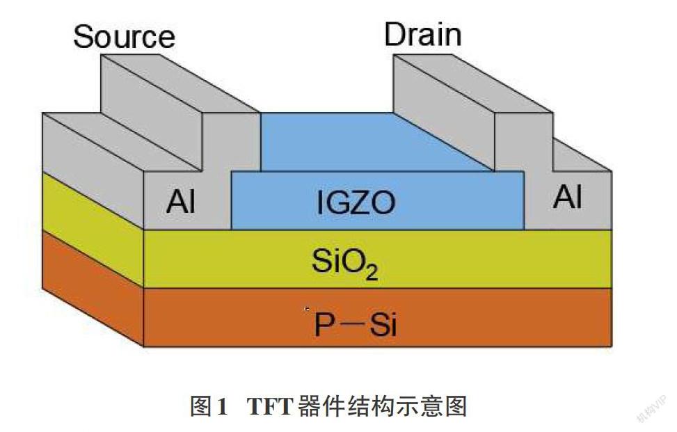
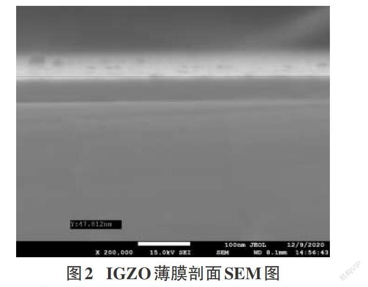
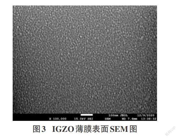
摘要:在室温条件下采用射频磁控溅射的方法在热氧化SiO2衬底上生长IGZO薄膜作为有源层,并将其制备为薄膜晶体管器件.研究不同的沟道长度对IGZO薄膜晶体管电学性能的影响.使用场发射扫描电子显微镜(SEM)表征IGZO薄膜的厚度,使用原子力显微镜(AFM)表征薄膜的表面形貌.实验结果表明,沟道长度对IGZO薄膜晶体管有着重要影响.当沟道长度为10[μm]时,IGZO薄膜晶体管的开关电流比达到1.07×10⁸,载流子迁移率为3.81cm2/V,阈值电压为27V,亚阈值摆幅为2V/dec.
关键词:IGZO;薄膜晶体管;磁控溅射;沟道长度
中图分类号:TB383 文献标识码:A
文章编号:1009-3044(2021)26-0138-03
开放科学(资源服务)标识码(OSID):
The Influence of Channel Length on the Performance of IGZO Thin Film Transistors
LIU Lu, GAO Xiao-hong, MENG Bing, FU Yu, SUN Yu-xuan, WANG Sen, LIU Yu-fei, HU Ding-wang
(Jilin Jianzhu University, Changchun 130119, China)
Abstract: At room temperature, using RF magnetron sputtering method to grow IGZO thin film as active layer on thermally oxidized SiO2 substrate, and prepare it into thin film transistor device. Study the influence of different channel length on the electrical performance of IGZO thin film transistor Use the field emission scanning electron microscope (SEM) to characterize the thickness of the IGZO film, and use the atomic force microscope (AFM) to characterize the surface morphology of the film. The experimental results show that the channel length has an important influence on the IGZO thin film transistor. When the channel length is 10 μm, the switching current ratio of the IGZO thin film transistor reaches 1.07×10⁸, the carrier mobility is 3.81 cm2/V, and the threshold voltage is 27V , The sub-threshold swing is 2V/dec.
Key words: IGZO; thin film transistors; magnetron sputtering; channel length
金屬氧化物半导体场效应晶体管近年来在高帧速、大尺寸、超高清晰平板显示器中引起广泛关注.与传统的非晶硅薄膜晶体管相比,金属氧化物基薄膜晶体管具有理想的场效应迁移率、较好的均匀性和稳定性和低工艺温度等优点[1, 2],能够满足有源矩阵有机发光二极管显示器高驱动电流的基本要求.金属氧化物半导体材料中,非晶氧化铟镓锌(IGZO)的性能最为突出,因此备受研究者们的关注[3]。
IGZO是一种n型半导体,带隙在3.5eV左右, 其组分中的In具有特别的外层电子结构会通过S轨道的重叠来运输载流子[4],有利于载流子的高速运输;Ga的掺入可以实现抑制薄膜晶体管沟道层中氧空位等本征缺陷,实现对载流子的调控. 2004年东京工业大学的Hosono等人首次报道了在室温条件下成功生长铟镓锌氧化物(IGZO)薄膜并应用于制备TFT器件,此后以IGZO为有源层的薄膜晶体管受到学术界和工业界越来越多的关注[5-6]。……