Plasmonic properties of graphene on uniaxially anisotropic substrates∗
2021-03-19ShengchuanWang汪圣川BinYou游斌RuiZhang张锐KuiHan韩奎XiaopengShen沈晓鹏andWeihuaWang王伟华
Shengchuan Wang(汪圣川), Bin You(游斌), Rui Zhang(张锐), Kui Han(韩奎),Xiaopeng Shen(沈晓鹏), and Weihua Wang(王伟华)
School of Materials and Physics,China University of Mining and Technology,Xuzhou 221116,China
Keywords: graphene,plasmonics,anisotropy,hexagonal boron nitride
1. Introduction
Graphene, a two-dimensional (2D) carbon crystal, since first produced by the group led by Geim through exfoliation procedures in 2004,[1]has attracted much attention from physical,chemical,and material communities. Graphene has many extraordinary electrical and optical properties,[2,3]including high optical absorptance, tunable surface conductivity,[4]and ultra-fast electron transport.[5]Due to its unique electronic band structure, graphene behaves like a metal at far infrared and terahertz (THz) frequencies, which could support collective excitations such as plasmons. It has been proved theoretically[6-10]and experimentally[11-13]that graphene plasmons have many promising characteristics, such as ultralong inherent lifetime, highly-confined electromagnetic field,huge local field enhancement, strong light absorption,[14-17]and relatively low loss.[18]However, the loss could be extremely increased with graphene placed on some substrates such as silicon dioxide,[19-21]much more than that in suspended graphene. To solve the issue,hexagonal boron nitride(hBN)can be chosen as the substrate,for example,plasmonic loss in graphene-hBN heterostructures is only about 20% of that in graphene-silicon structures.[18]
In addition to an ideal substrate for graphene, hBN has its own merit as an optical material. The hBN is a hyperbolic material in nature,[22]in which the dielectric constants are the same in plane(εxx=εyy=ε‖),but have opposite signs compared to that of out plane (ε‖·εzz=ε‖·ε⊥<0). Because of this property, hBN can be used in many fields to achieve peculiar optical response,[23]including negative refraction,[24]ultra-slow phase velocity, and nano-focusing.[25-31]Furthermore,graphene-hBN heterostructures support hybrid surfaceplasmon-phonon polariton modes, which could combine the advantages of graphene plasmons and surface phonons,[32]and similar to graphene plasmons, the hybrid modes can be further engineered through the structures and the doping of graphene.[33,34]Very recently, such heterostructure has been demonstrated as a prominent platform for investigating physics under extreme conditions, for instance plasmonic in nanoscale cavities[35,36]and electron scattering at arbitrarily low energies,[37]and designing photoelectric devices with diverse functionalities, such as ultrafast Zener-Klein transistor,[38]high-performance polarization splitter,[39]and active plasmonic switch.[40]
On the other hand, the screening effect of isotropic substrate on graphene plasmons is well known (resonance frequency inversely proportional to dielectric constant),but hBN is a uniaxially anisotropic material. The anisotropy could change the behavior of graphene plasmons,thus provides another route to manipulate the plasmonic resonances.[41]However, most of the previous works only utilize the 2D nature of hBN and its lattice matching with graphene. The effects of anisotropic and hyperbolic properties of hBN on graphene plasmonic excitations are still not well understood,especially at epsilon-near-zero (ENZ) band. Obviously, promoting the relevant understanding is quite beneficial, which will essentially enrich the studies of graphene plasmonics and pave the way for related device applications. In this work, we mainly discuss the plasmonic properties of graphene nanoribbons on uniaxially anisotropic substrates,and especially as the components of dielectric constant approaching zero from both positive and negative sides. Such anisotropic dielectric substrates can be easily achieved in hBN at THz frequency region,which provides experimental possibilities of our work.
2. Theoretical model of graphene on uniaxially anisotropic substrate
Similar to noble metals, graphene also supports collective excitations,which are transverse magnetic(TM)polarized surface modes as well. In this part,we are going to study the fundamental properties of graphene plasmons as described in Fig.1. The graphene nanoribbon array is placed on a uniaxially anisotropic substrate,[42]whose dielectric matrix can be expressed as a tensor
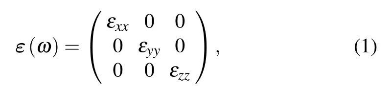
with εxx=εyy=ε‖and εzz=ε⊥. Above graphene,there is an isotropic medium with dielectric constant εr. In the region of z >0,the TM modes can be assumed to have the form

and the electromagnetic fields in z <0 region (inside the anisotropic substrate)can be expressed as
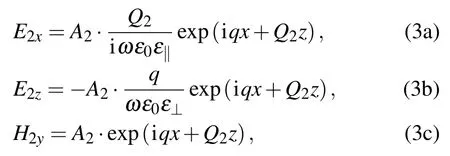
where the wave vectors in z direction are given by

After matching the boundary conditions at z=0 for electric field Exand magnetic field Hy:
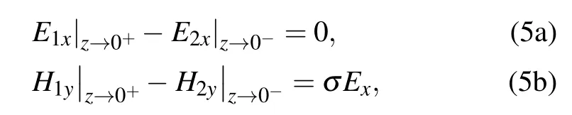
we obtain the dispersion relation for the TM modes
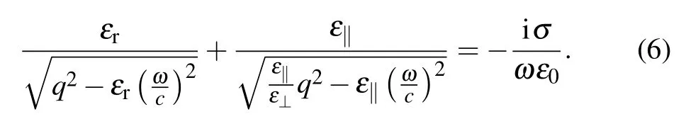
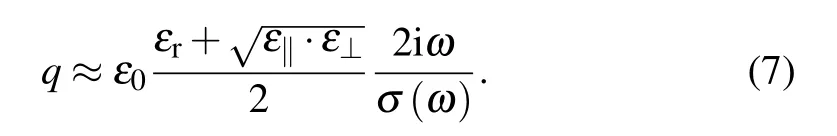
By explicitly writing the dependence of the conductivity on the wave vector q, it is possible to study nonlocal optical response, where the mean free path of electrons can be smaller than q−1. Throughout this work,we consider the nonretarded regime(q≫ω/c),so equation(6)can be simplified to
Here,σ(ω)is the surface conductivity of 2D graphene,which can be obtained from the linear response theory(so-called random phase approximation, RPA).[43]As the structures are up to hundreds of nanometers in size, their optical response is mostly determined by the leading term of the surface conductivity,and thus σ(ω)can be approximately reduced to a simple Drude form[44]
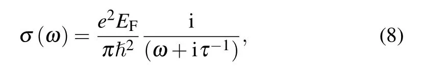
with EFthe Fermi level and τ the relaxation time. This Drude surface conductivity is used throughout our work,and the parameters EF=0.4 eV,τ=0.5 ps.[45]However,we should emphasize that the quantum size effect and edge effect of optical response are ignored in our modelling, which will be extremely important as the structures scale down to tens of nanometers.[43,46]While in structures of hundreds of nanometers,the common treatment based on classical electromagnetic theory will give reliable results.
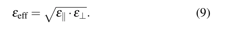
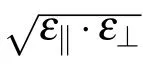
Comparing with the well-known graphene dispersion relation,[47]we can easily obtain the effective dielectric constant of the anisotropic substrate[48]
This theoretical formula only applies to semi-infinite substrates, and the dielectric components in all directions should be great than zero. It does not fit the Restatrahlen bands in hBN,[49]in which the eigenstates should be guided waves instead of plane waves. Using the dispersion relationship Eq. (7), we are able to estimate the plasmonic resonance frequencies for given wave vector q. The procedure can be easily performed in the structures with high symmetry,for example,in disks of radius R, q=n/R,[50]and in ribbons of width W,q=nπ/W,[51]where n is the order of plasmonic modes.
In order to verify such a simple formula, we calculate the plasmonic resonance frequencies in graphene nanoribbons by means of full wave simulations, in which the plasmonic resonance frequencies can be extracted from the positions of the absorption peaks. In practice, the commercial finite element computation package COMSOL MULTIPHYSICS is employed for all full wave simulations. Because of the threedimensional(3D)modelling requirement, graphene is treated as a transitional boundary condition (TBC), with an artificial thickness tg(sufficiently small compared to the lateral size,tg=0.5 nm throughout the work) and thus an effective 3D permittivity[52]

Since graphene ribbons possess translational invariance along y direction,it is sufficient to investigate field scattering in the plane of cross section, namely, x-z plane (see Fig.1). In practice, we place a single graphene ribbon (one-unit cell) in the center of a square waveguide, with the periodic boundary condition (PBC) in x direction and two ports in z direction.And then, the absorption spectra can be calculated from Sparameter. In such modelling, the anisotropic substrate can be directly implemented through the material setting, for instance,assigning different values to the diagonal terms in the matrix of dielectric constant.In order to simplify the following discussion,the effects of ε‖and ε⊥are investigated separately,for instance, as studying the effect of ε‖, the value of ε⊥is fixed to be 1, and vice versa. In particular, the variable component of permittivity is varied by either increasing from 1 to 10 or decreasing from 1 to 0(epsilon-near-zero,ENZ).For the permittivity exactly being 0,a tiny imaginary part of the order of 10−5is introduced for the convergence requirement of the simulations.
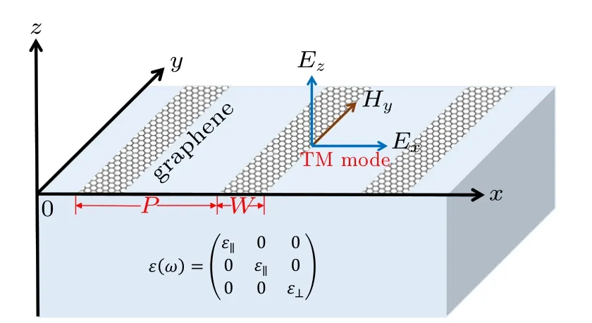
Fig.1. Schematic diagram of an array of graphene nanoribbons on a uniaxially anisotropic substrate,and the TM mode with magnetic field along the ribbons. The width of graphene ribbons W =100 nm and the period of the array P=300 nm throughout the work expect noted otherwise. The graphene ribbons are infinitely long which indicates translational invariance along y direction.
For the case of a single interface (ribbons of width W =100 nm and period P=300 nm on a semi-infinite substrate),the results obtained from simulations (dots) and the formula(solid curves) are shown in Fig.2, in which region I (blue shaded) is for ε‖>ε⊥and region II (pink shaded) is for ε‖<ε⊥. It is clear that the results from the formula show very good agreement with those from simulations,which confirms the validity of the formula. Furthermore, it can be seen that the curves from two figures are exactly consistent. Such consequence can be easily understood from the formula, in which the effective dielectric constant depends on the product of permittivities in parallel ε‖and in perpendicular direction ε⊥. However, the electric field distributions for the two situations are very different. In anisotropic substrates,the electric fields decay rapidly in the direction of low dielectric constant,which thereby causes energy concentrated in another direction.[53]When ε‖<ε⊥(see Fig.2(c)), the electric fields penetrate deeper into the substrate, while ε‖>ε⊥(see Fig.2(d)), the electric fields are more concentrated at the interface. This can also be explained by Eq.(4b)that as ε‖<ε⊥,Q2is relatively small and thus the electric field decays away from the interface slowly.
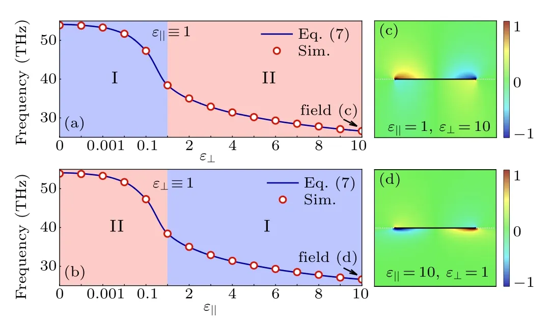
Fig.2. The plasmonic frequencies as the function of ε⊥(a)and as the function of ε‖ (b), obtained from Eq.(7)and full wave simulations, in case of a semi-infinite substrate. Region I (blue shaded) for ε‖ >ε⊥and region II (pink shaded) for ε‖ <ε⊥. (c) and (d) The electric field distributions at situations marked in(a)and(b).
In reality, the substrates can not be semi-infinite. If the substrates are not thick enough, the corresponding thickness will affect the plasmonic properties, and apparently the resonance frequencies. In order to study this effect, we take the substrate thickness of 300 nm, 200 nm, and 100 nm for numerical simulations. The corresponding simulation results are shown in Fig.3. Compared to the theoretical curve(obtained from the formula), the dots exhibit obvious deviations when reducing the thickness of the substrate. For fixed values of ε⊥and ε‖, the deviations are more significant for smaller thickness. However,the largest deviation of each thickness occurs at different regions. Since the theoretical curve is for a semiinfinite substrate, or equivalently a slab of infinite thickness,the results here indicate that the impact of thickness depends on the values of ε⊥and ε‖. In fact, such phenomena can be easily explained by the argument above. The impact of the thickness relies on the direction of energy concentration. If the energy penetrates deeper into the substrate, the thickness will play a more important role. To achieve such a consequence, the dielectric constant ε⊥should be larger than the dielectric constant ε‖(region II in Figs. 3(a) and 3(b)). In Fig.3(a) ε‖=1, and thus ε⊥should be larger than 1, while in Fig.3(b)ε⊥=1,and similarly ε‖should be smaller than 1.However,if both ε⊥and ε‖locate roughly from 1 to 4,100 nm would be thick enough,and the impact of the thickness could be ignored.
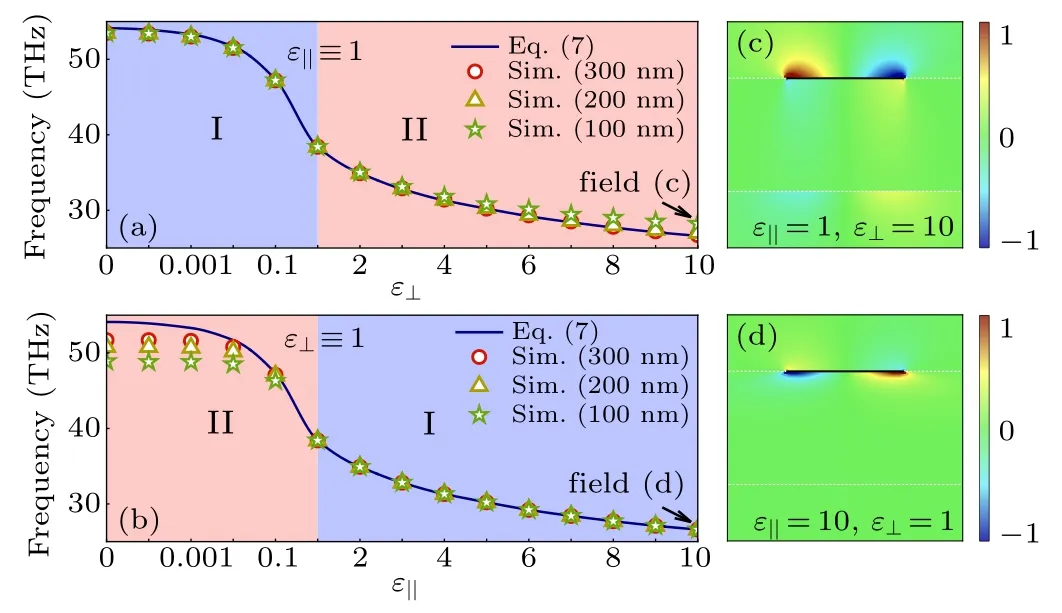
Fig.3. The plasmonic frequencies as the function of ε⊥(a)and as the function of ε‖ (b), in case of the finite substrates with thicknesses of 300 nm,200 nm,and 100 nm. Region I(blue shaded)for ε‖>ε⊥and region II(pink shaded)for ε‖<ε⊥. (c)and(d)The electric field distributions at the situations marked in(a)and(b).
As is well known,the most appealing feature of graphene plasmons is its active tunability by an external gate voltage.Specifically,the plasmonic properties will be varied for different Fermi level which is involved in surface conductivity(see Eq. (8)). Thus, it is very necessary to extend recent studies to structures with different Fermi level. We compute the resonance frequencies of graphene ribbons on hBN of 100 nm thickness (see Fig.1 for other parameters). The results are shown in Fig.4. It is clear that for both situations, the spectrum will globally shift up with increasing Fermi level and down with decreasing Fermi level. Meanwhile, the asymptotic behaviors at two limits, namely, large epsilon and ENZ,are also reserved as comparing with Fig.3.
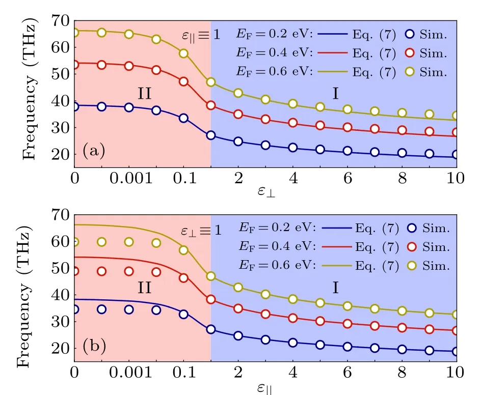
Fig.4. Resonance frequencies as the functions of ε⊥(a)and ε‖ (b),in graphene ribbons with the Fermi level of 0.2 eV(blue curves), 0.4 eV(red curves), and 0.6 eV (brown curves). The thickness of the hBN dielectric layer is set to 100 nm for all calculations.
So far, we have discussed in detail the evolution of graphene plasmons as the function of non-negative dielectric components of the substrates.However,if one of the dielectric components is negative (hyperbolic material), the plasmonic properties would be changed dramatically due to the strong Coulomb screening. But if either ε⊥or ε‖is of a very small negative value, they will also lead to different consequences.For substrates of thickness 100 nm,the other parameters consistent with the above discussions, the simulation results are shown in Fig.5. It is clear that inside the hyperbolic material, the graphene plasmons are not bounded to the interface,but can propagate inside the hyperbolic slab. These modes are actually phonon-polariton modes,[54]guided in the slab. For non-magnetic media,the condition of the propagation solution in hyperbolic materials asymptotically approaches[55]

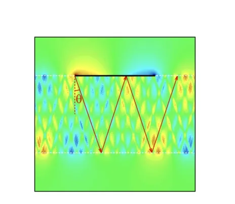
Fig.5. Electric field distributions in graphene nanoribbons on 100 nm thick uniaxially anisotropic substrates. θ is the refractive angle of the guide wave inside the hyperbolic slab.
3. Graphene on hBN

Hexagonal boron nitride is a promising substrate for graphene. Since matching the lattice, the carrier mobility of graphene on hBN can be one order larger than that of graphene on silicon dioxide (SiO2).[56]Furthermore, hBN is a uniaxial anisotropic material, and a nature hyperbolic material at specific frequency region.[57]Thus the above discussions have lots of practical significance. In hBN, there are transverse(ωTO)and longitude optical phonons(ωLO),which determine its optical response,for example,the Lorentz-like expressions of dielectric functions given by[58]Here, the parameters are as follows: ε∞,‖= 4.87, ωTO,‖=41.1 THz,ωLO,‖=48.3 THz,Γ‖=15.0 THz,and ε∞,⊥=2.95,ωTO,⊥=23.4 THz,ωLO,⊥=24.9 THz,Γ⊥=12.0 THz.These two dielectric components are plotted in Fig.6. At a large frequency region, hBN is a uniaxially anisotropic material with positive ε⊥and ε‖, and only exhibits hyperbolic behaviour at two isolated Restatrahlen bands (close to ω =ωLO,‖and ω =ωLO,⊥), where we can also find the frequency regions of epsilon-near-zero (insets shown in Fig.6). Hence, hBN also provides a platform for studying plasmonic properties as graphene on a uniaxial epsilon-near-zero substrate.
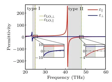
Fig.6. Dispersion of two dielectric components of hBN, type I and type II Restatrahlen bands are shaded,dashed lines plot longitude optical phonon frequencies(epsilon-near-zero,ENZ regions).
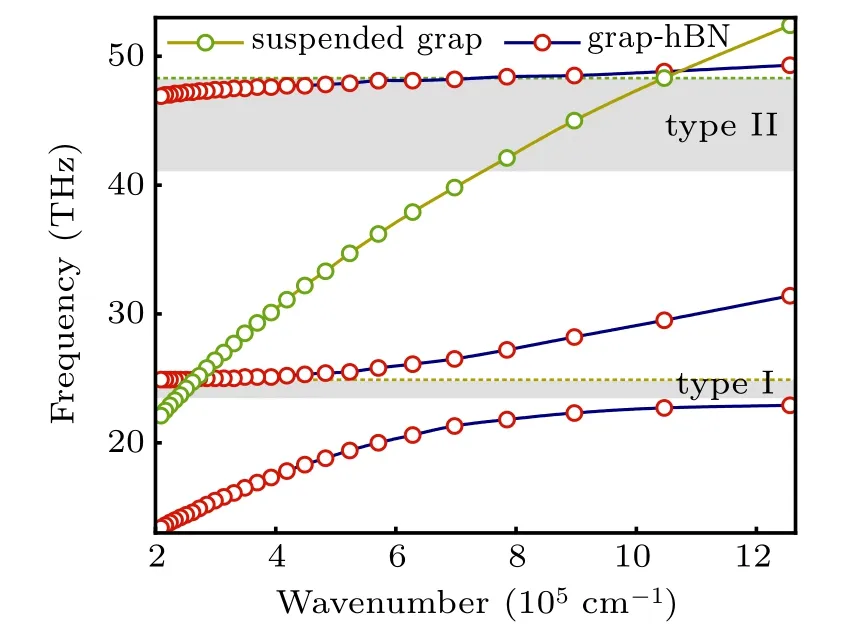
Fig.7. Plasmonic dispersions in suspended graphene (green dotted)and in graphene-hBN heterostructure(red dotted). HBN has thickness 100 nm as above.
In order to examine further the plasmonic behavior when one of the dielectric components being a very small negative number(see Fig.5),we map the plasmonic dispersion of graphene-hBN heterostructures (100 nm thickness as above)in Fig.7,where the width W of graphene ribbons varies from 25 nm to 150 nm, and the period is three times the width.As before, we extract the plasmonic frequencies from simulations and the equivalent wavevector can be obtained through q=nπ/W (see illustration in Section 2). Compared to the plasmonic dispersion of suspended graphene (green dotted curve), the plasmonic dispersion of graphene-hBN is divided into three parts by two Reststrahlen bands of hBN (red dotted curves). It is clear that near the Reststrahlen band of type II, with varying the width of the ribbon, the dispersion curve crosses the epsilon-near-zero frequency band (dashed lines).The results presented here are consistent with the numerical simulation results shown in Fig.5.
4. Conclusion
猜你喜欢
杂志排行
Chinese Physics B的其它文章
- Transport property of inhomogeneous strained graphene∗
- Beam steering characteristics in high-power quantum-cascade lasers emitting at ~4.6µm∗
- Multi-scale molecular dynamics simulations and applications on mechanosensitive proteins of integrins∗
- Enhanced spin-orbit torque efficiency in Pt100−xNix alloy based magnetic bilayer∗
- Soliton interactions and asymptotic state analysis in a discrete nonlocal nonlinear self-dual network equation of reverse-space type∗
- Discontinuous event-trigger scheme for global stabilization of state-dependent switching neural networks with communication delay∗