Analysis of non-uniform hetero-gate-dielectric dual-material control gate TFET for suppressing ambipolar nature and improving radio-frequency performance∗
2019-11-06HuiFangXu许会芳JianCui崔健WenSun孙雯andXinFengHan韩新风
Hui-Fang Xu(许会芳),Jian Cui(崔健),Wen Sun(孙雯),and Xin-Feng Han(韩新风)
Institute of Electrical and Electronic Engineering,Anhui Science and Technology University,Fengyang 233100,China
Keywords:non-uniform gate–oxide layer,ambipolar current,radio-frequency performances,tunnel fieldeffect transistor
1.Introduction
In order to be better applied to integrated circuits,reduce the cost,and improve the on-state current(Ion)and high-frequency characteristics,the size of device needs to be reduced continuously. However,downscaling of the device leads to the increased power dissipation in electronic circuits because of increased leakage current in the off-state.As far as the traditional metal–oxide–semiconductor fieldeffect transistor(MOSFET)is concerned,it is very difficult to reduce the supply voltage for the purpose of preventing power from dissipating due to the minimum achievable thermionic emission limit of the subthreshold swing(SS)(SS=60 mV/decade)and large off-state current(Ioff).The appearance of tunnel field-effect transistor(TFET)is consistent with the trend of the continuous downsizing of devices for future ultralow power dissipation integrated circuit applications.The TFET can achieve an SS value less than 60 mV/decade at room temperature due to the fact that the carrier injection of the device from source region to channel region is based on band-to-band tunneling(BTBT).[1]Moreover,the TFET can offer other advantages such as low Ioffwhen the barrier width at the source-channel junction is very large in the off-state,[2–4]high immunity against short-channel effects(SCEs),and small supply voltage below 0.5 V.[5,6]However,the TFET has some shortcomings such as low Ion,ambipolar current(Iamb),and large Miller capacitance. The Ionshould be enhanced and ambipolar behavior and Miller capacitance should be well reduced in order to make TFET a better application prospect in the future integrated circuit.Therefore,researchers should comprehensively carry forward the advantages of TFET and overcome its shortcomings. Up to now,many techniques have been proposed to improve Ion,such as narrow bandgap materials,[7–11]high-k gate dielectric,[12]hetero-junction mechanism,[13,14]and doping-less TFETs,[15]source-side pocket doping,[16]hetero-stacked TFET,[17]heteromaterial gate,[18,19]etc. The Iambcan be reduced by using the dual-material control-gate(DMCG)TFETs,[20]charge plasma-based TFETs with gate engineering,[21,22]gate material workfunction engineering,[23]lightly doped drain,[24]and gate–drain underlap structure.[25,26]Moreover,a hetero-gatedielectric(HGD)TFET with a high gate–oxide dielectric near the source side and a low gate–oxide dielectric near the drain side can enhance Ionand obtain promising radio frequency performance.[27–29]
The downscaling of gate–oxide layer thickness is an important method to enhance the steep switching characteristics of TFETs. But it also leads to large gate leakage current.Moreover,the thickness of the gate–oxide layer is assumed to be uniform in almost all existing TFET devices.Therefore,it is necessary to study the variation of the TFET characteristics in the case of non-uniform gate–oxide layer thickness. The non-uniform structure is defined as a structure whose gate–oxide thickness is thinner on the source-channel side while larger gate–oxide thickness on the drain-channel side. Recently,a TFET with non-uniform gate–oxide shape and an asymmetric hetero-dielectric engineered dual-material double gate(DG)TFET has been analyzed.[30,31]In the present work,a novel device is proposed by combining various advantages together such as non-uniform gate–oxide shape,HGD and DMCG,and named NDMCG TFET.It is intended that in the proposed device the Iambvalue can be reduced,the on-off current ratio can be enhanced,and the radio-frequency(RF)performance can be improved by optimizing the structural parameters of device.
2.Device structure
The structure of NDMCG TFET is shown in Fig.1.The gates closer to the source and the drain are denoted as G(tunneling gate)and G2(auxiliary gate),respectively. The gate between G and G2is marked as G1(control gate).In the proposed device,the work function of G is selected to be the same as that of G2,but their work functions are less than that of G1.The parameters used in the following simulations are P+source,channel,and N+drain,and they are doped with concentration 1020cm−3,1016cm−3,and 5×1019cm−3,respectively.The thickness of silicon(tsi)is 10 nm,the thickness of HfO2(t1)and the maximum thickness of SiO2(t2)are 1 nm and 3 nm,respectively.The length of P+source(Ls),channel(Lch),and N+drain(Ld)are 50 nm,50 nm,and 50 nm,respectively.The length of HfO2,G,G1,and G2are Lox,L1,L2,and L3,respectively.

Fig.1. Structure of non-uniform gate–oxide layer hetero-gate-dielectric DMCG TFET.
The simulations are performed by using silvaco atlas simulator,[32]and the models such as dynamic nonlocal bandto-band tunneling model,Shockley–Read–Hall model,auger recombination model,bandgap narrowing model,and Fermi statistics model are used in this work. The dynamic nonlocal band-to-band tunneling model is an important model in describing the operating principle of TFET.Using the Kane model,[33]the band-to-band tunneling generation rate is expressed as[34]
where A and B are the tunneling parameters,which are 4×1014cm−1/2·V−5/2·s−1and 1.9×10⁷V/cm,respectively;[32]E is the lateral electrical field;D is a material-dependent constant,which is 2 and 2.5 for the direct and indirect band-gap materials,respectively.The values of Ion,Ioff,and Iambdefined at Vgs=0.8 V,0 V,and −0.5 V respectively are calculated when Vdsis fixed at 0.5 V,here Vgsand Vdsare the gate–source voltage and drain–source voltage,respectively.
3.Results and discussions
3.1.Performance comparison between NDMCG TFET and DMCG TFET
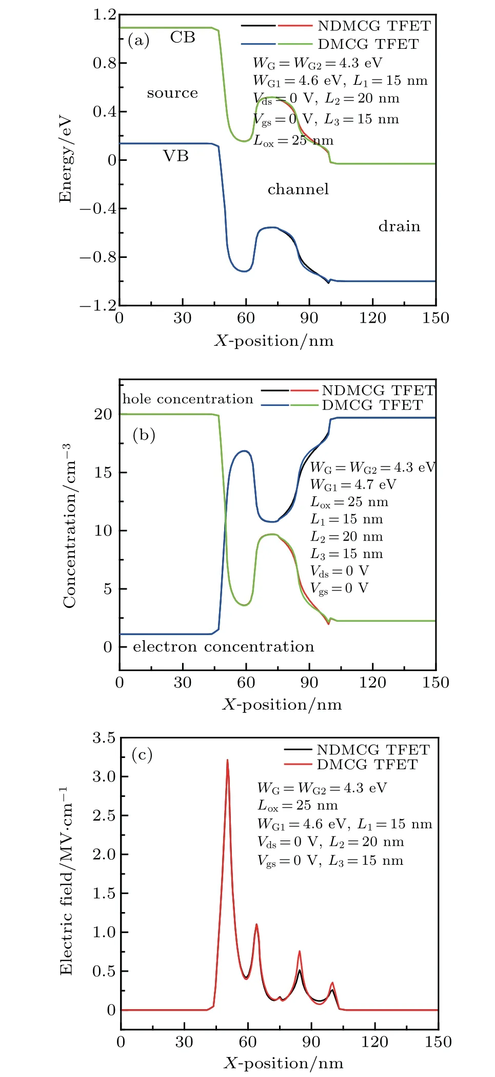
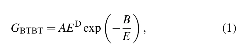
Fig.2.Comparisons of curves of(a)energy band,(b)carrier concentration,and(c)electric field versus X pointion between NDMCG TFET and DMCG TFET under thermal equilibrium state.
Figure 2 shows the energy band,carrier concentration,and electric field for two devices under thermal equilibrium state.From Fig.2(a),it can be found that there is no change of the tunneling distance at the source/channel interface since the modification is made on the channel close to the drain side.However,the increased tunneling barrier at the drain/channel junction can be seen for the NDMCG TFET.The NDMCG TFET provides higher hole concentration and lower electron concentration than the DMCG TFET as shown in Fig.2(b).Hence,the electric field varies at the drain/channel junction along the lateral direction between NDMCG TFET and DMCG TFET as shown in Fig.2(c).The reduced electric field can be observed for the NDMCG TFET due to the varying band levels and the different carrier concentrations.
Fig.3.Comparisons(a)energy band under ambipolar state,(b)transfer characteristics,and(c)subthreshold swing between NDMCG TFET and DMCG TFET.
Figure 3 shows the energy bands under ambipolar state,transfer characteristics,and SS for two devices.It can be seen that the tunneling width of NDMCG TFET is larger than that of the DMCG TFET at the drain/channel junction under ambipolar state,which can limit the number of holes to tunnel from the drain to the channel.Therefore,the NDMCG TFET can reduce the ambipolar current as depicted in Fig.3(b).The SS as a function of Idsis shown in Fig.3(c).It can be seen that the extracted SS behavior appears relatively gradual lasting nearly 4 orders of magnitude of drain current variation.But it is worth noting that the two devices show little difference in SS.This is mainly due to the fact that the non-uniform gate–oxide shape of NDMCG TFET is made on the channel close to the drain side,so it has little effect on the ∆GBTBTincreament as well as on the drain current increament ∆logIdswith Vgsincreasing.
3.2.Optimization of ,and for NDMCG TFET
This subsection is dedicated to the study of the influence of variation in L2on Ionand Iofffor NDMCG TFET as depicted in Fig.4(a).In this case,L1is fixed at 15 nm.The increase in L2leads to the reduction of Ionwhen the length of L2is larger than 5 nm. Moreover,the NDMCG TFET can generate optimum results of Ioffand Ionwhen L2is fixed at 10 nm.The Iambfor NDMCG TFET is less than that for the DMCG TFET because the tunneling width of NDMCG TFET is larger than that of the DMCG TFET at the drain/channel junction,hence tunneling of carriers from drain to channel is reduced,resulting in reduced Iambas shown in Fig.4(b).Therefore,we can conclude that the proposed device provides a decent amount of suppression in Iamband large on-off current ratio when L1,L2,and L3are 15,10,and 25 nm,respectively.
Figure 5(a)is dedicated to the study of the influence of variation in L1on Ionand Iofffor NDMCG TFET.In this case,L3is fixed at 15 nm. The NDMCG TFET can generate a large on-off current ratio when L1is 15 nm. However,Iambfor NDMCG TFET is not significantly degraded with variation in L1since the energy band at the drain/channel junction hardly changes under these conditions as indicated in Fig.5(b). The Iambfor NDMCG TFET is less than that for DMCG TFET,which is due to the fact that the tunneling width of NDMCG TFET is larger than that of the DMCG TFET at the drain/channel junction.Hence,we can infer that selecting L1=15 nm along with L2=20 nm and L3=15 nm provides a decent amount of suppression in Iamband large on-off current ratio.Based on the preceding analysis,it is clear that the optimized dual-material control-gate lengths(L1,L2,L3)are 15,10,25 nm and 15,20,15 nm in terms of suppression in Iamband large on-off current ratio.
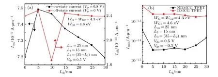
Fig.4.(a)Ion and Ioff varying with L2 for NDMCG TFET,and(b)Iamb varying with L2 for NDMCG TFET and DMCG TFET.
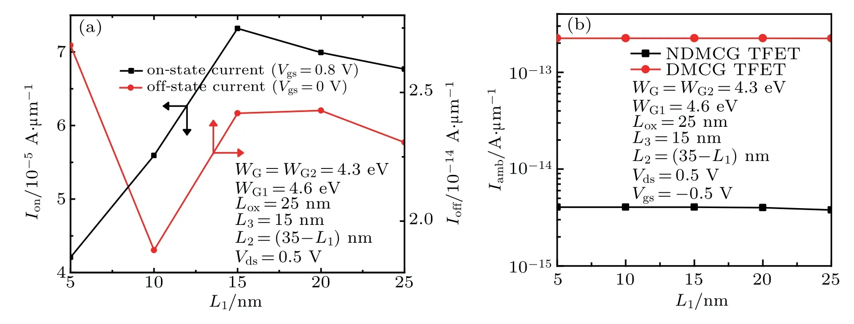
Fig.5.(a)Ion and Ioff varying with L1 for NDMCG TFET,and(b)Iamb varying with L1 for NDMCG TFET and DMCG TFET.
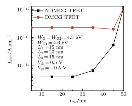
Fig.6.Iamb varying with Lox for NDMCG TFET and DMCG TFET.
Figure 6 shows the influence of variation in Loxon Iambfor NDMCG TFET and DMCG TFET when L1,L2,and L3are fixed at 15,20,and 15 nm,respectively.It is expected that as Iambincreases the Loxincreases because the gate control is strengthened.Moreover,when the length of Loxis longer than 35 nm,Iambis increased sharply.It should be noted that the length of Loxis 50 nm,which represents the uniform HfO2case(t1=t2=1 nm).The proposed device can generate small Iambespecially when Loxis less than 35 nm.Generally speaking,suppression in Iamband large on-off current ratio can be obtained by optimizing L1,L2,L3,and Loxfor the NDMCG TFET,but the optimized device has not achieved superior performance about SS compared with the DMCG TFET.However,a hetero-stacked TFET with stacked source configuration can effectively suppress the SS degradation behavior and obtain a steeper average SS by self-adaptive current replenishing with bandgap engineering.[17,35]The optimization of SS for the NDMCG TFET is not considered and it will be dealt with in our subsequent work.
3.3.Parasitic capacitance and radio-frequency performance for NDMCG TFET
This subsection is dedicated to the study of the influence of variation in L3,and L1on the gate–drain capacitance(Cgd)of NDMCG TFET as depicted in Fig.7.The increase in Cgdwith Vgsis due to the formation of an inversion layer in the channel region from the drain to the source.Moreover,Cgdis dominated by the inversion capacitance in the on-state.The increase of L3in Fig.7(a)or L1in Fig.7(b)represents the decrease of L2in the proposed device.Therefore,the effect of control gate’s work function on the threshold voltage of the device becomes smaller with L2decreasing. The threshold voltage of the proposed device decreases,which leads to an increase in charge and ultimately an increase in capacitance.
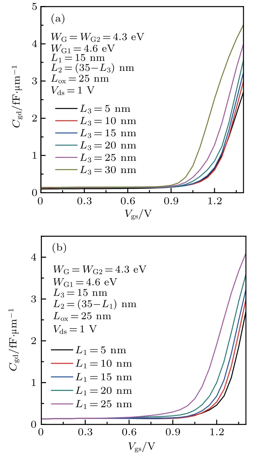
Fig.7.Cgd varying with(a)L3 and(b)L1 for NDMCG TFET.
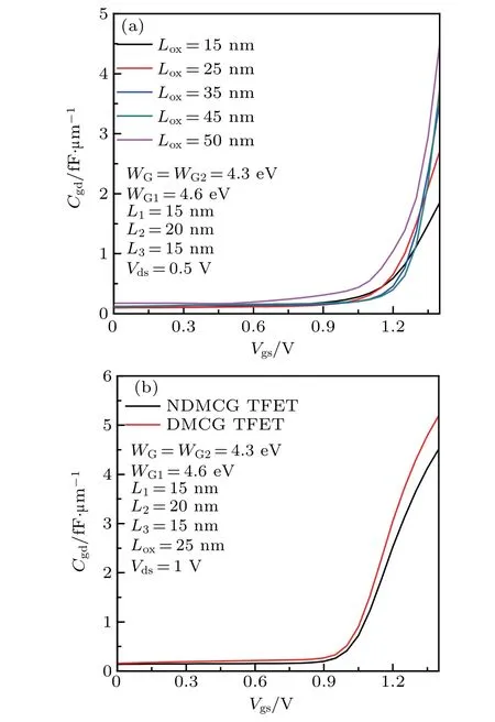
Fig.8.(a)Cgd–Vgs curves for NDMCG TFET with different values of Lox,and(b)comparison of Cgd–Vgs curve between NDMCG TFET and DMCG TFET.

Fig.9.Curves of(a)GBP,(b)ft,(c)τ,and(d)TFP versus Vgs of NDMCG TFET for different values of L3.
Figure 8(a)shows the variation of Cgdwith Vgsfor NDMCG TFET with L1,L2,and L3being 15,20,and 15 nm,respectively.It can be found that Cgdincreases with Loxincreasing,which is due to the fact that the gate–oxide thickness near the drain region is varied.This effect indicates the importance of the design of non-uniform gate–oxide layer.Moreover,non-uniform gate–oxide layer can reduce the coupling between the gate and the drain regions,thereby reducing Cgd.The Cgdof NDMCG TFET is less than that of DMCG TFET under all the same conditions as shown in Fig.8(b).Therefore,The NDMCG TFET can better control the gate over the channel region.
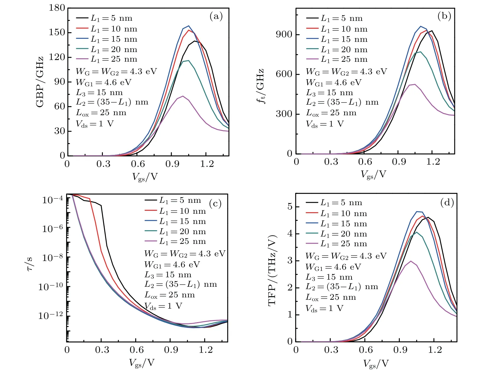
Fig.10.Curves of(a)GBP,(b)ft,(c)τ,and(d)TFP versus Vgs for NDMCG TFET with different values of L1.
Figure 11 shows the influences of variation in Loxon GBP,ft,τ,and TFP for NDMCG TFET,with L1,L2,and L3fixed at 15,20,and 15 nm,respectively.It can be found that the maximum values of GBP,ft,and TFP increase with the value of Loxincreasing,but the values of three parameters described above decrease when the length of Loxis 50 nm.It should be noted that the length of Loxis 50 nm,which represents the uniform HfO2case(t1=t2=1 nm).The proposed device embodies the advantages of non-uniform hetero-gate-dielectric in terms of three parameters,and an optimum value(Lox=45 nm)exists at which the parameters are maximum.It is worth noting that there is little difference among the three parameters when Loxis 45 nm and 35 nm,separately.By combining with the analysis results of Fig.6,the optimum value of Loxis obtained to be 35 nm.But the difference in transit time is not obvious in the above cases.
Figure 12 shows comparison of curves of GBP,ft,τ,and TFP versus Vgsbetween NDMCG TFET and DMCG TFET,with Lox,L1,L2,and L3fixed at 35,15,20,and 15 nm,respectively. The results show that the NDMCG TFET has a better RF performance than the conventional DMCG TFET.High GBP implies larger gain as well as bandwidth,the increase in ftresults in small switching delay.All these results demonstrate that the proposed device has a better prospect of high-speed and high-frequency applications in the advanced integrated circuits.
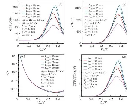
Fig.11.Curves of(a)GBP,(b)ft,(c)τ,and(d)TFP versus Vgs for NDMCG TFET with different values of Lox.
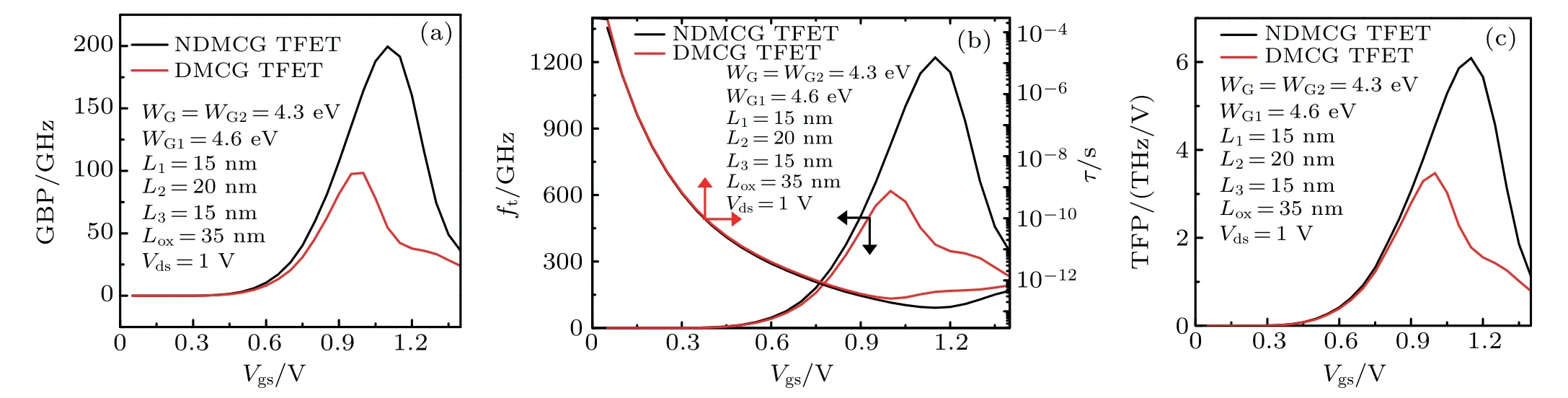
Fig.12.Comparison of curves of(a)GBP,(b)ft,τ,and(c)TFP versus Vgs between NDMCG TFET and DMCG TFET,with Vds fixed at 1 V.
The above-mentioned parasitic capacitance and RF parameters for TFETs are analyzed when Vdsis 1 V,and the maximum values for GBP,ft,and TFP are achieved when Vgsis nearly 1.1 V.However,according to the projection of International Technology Roadmap for Semiconductor(ITRS),the TFET has a great potential for low-power applications.In this case,Vdsis lower than 1 V.Therefore,the device optimization is also analyzed when Vdsis fixed at 0.5 V as indicated in Fig.13,from which we can infer that the NDMCG TFET enhances the RF parameters compared with the conventional DMCG TFET under lower power supply voltage.Moreover,the maximum values for GBP,ft,and TFP are achieved when Vgsis nearly 0.7 V.Therefore,the proposed device is also suitable for power supply voltage applications.
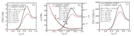
Fig.13.Comparison of curves of(a)GBP,(b)ft,τ,and(c)TFP versus Vgs between NDMCG TFET and DMCG TFET,with Vds fixed at 0.5 V.
4.Conclusions
The performances of NDMCG TFET are studied based on TCAD simulations. We demonstrate that the increase of Loxaffects Iamb,but has little effect on Ionand Ioff.The results show that the design of a non-uniform gate–oxide layer with Loxbeing 35 nm and the dual-material control-gate lengths L1,L2,and L3being respectively 15,20,15 nm can realize high Ion/Ioffand RF parameters with relatively low value of Iamb. When the drain–source voltage is fixed at 1 V for the optimized device,the RF parameters GBP,ft,and TFP are investigated,of which the maximum values are 199 GHz,1.2 THz,and 6.1 THz,respectively.Moreover,the RF parameters of the NDMCG TFET are enhanced compared with those of the conventional DMCG TFET under lower power supply voltage.The results indicate that the NDMCG TFET has the great potential applications in high-performance RF component,which should be the superiority in future high-frequency,and high-switching-speed electronics applications.
杂志排行

Chinese Physics B的其它文章
- Compact finite difference schemes for the backward fractional Feynman–Kac equation with fractional substantial derivative*
- Exact solutions of a(2+1)-dimensional extended shallow water wave equation∗
- Lump-type solutions of a generalized Kadomtsev–Petviashvili equation in(3+1)-dimensions∗
- Time evolution of angular momentum coherent state derived by virtue of entangled state representation and a new binomial theorem∗
- Boundary states for entanglement robustness under dephasing and bit flip channels*
- Manipulating transition of a two-component Bose–Einstein condensate with a weak δ-shaped laser∗