Ⅲ-族氮化物半导体的研究进展
2015-01-12李钟玉兰云军
韩 波,李钟玉,兰云军
(温州大学化学与材料工程学院,浙江 温州 325035)
Ⅲ-族氮化物半导体的研究进展
韩 波,李钟玉,兰云军
(温州大学化学与材料工程学院,浙江 温州 325035)
近年来,Ⅲ-族氮化物材料引起了科学工作者的极大兴趣,并取得了重大的进展。本文介绍了Ⅲ-族氮化物材料和器件的发展,评述了Ⅲ-族氮化物的掺杂和Ⅲ-族氮化物合金的研究现状。最后,简要展望了Ⅲ-族氮化物未来的应用潜能。
Ⅲ-族氮化物 ;半导体;研究进展
Ⅲ-N基半导体是一类重要的光电功能材料,具有较宽的带隙,它们的透光范围可以从紫外光区一直延伸到近红外光区。同时,它们还具有较低的压缩性、较高的导热性以及良好的化学稳定性,相比大多数镉化合物半导体材料,Ⅲ-N基类半导体材料毒性更低。这些突出的物理和化学性质使其成为一类备受关注的光电功能材料。1962年GaAs激光二极管的问世,拉开了对Ⅲ-V族材料特别是GaN和InN以及他们的固溶体等研究开发的序幕。以GaN、InN等为代表的第三代半导体宽禁带化合物比以前的半导体材料有更大的优势和应用前景,成为21世纪初最活跃的半导体材料体系。表1列出了300K下二元氮化物的一些基本属性。
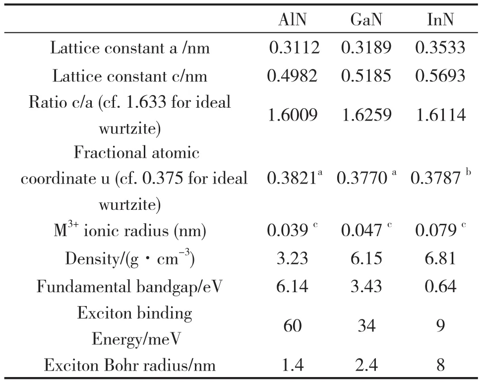
表1 300K下二元氮化物的基本属性Table 1 the properities of binary nitride under 300k
1 Ⅲ-族氮化物材料和器件的发展
Ⅲ-族氮化物材料被广泛用于光电子器件,如发光二极管(LED)、激光二极管(LD)、紫外线(UV)检测器、太阳能电池、表面声波装置、高温和高频率的场效应晶体管(FET)、异质结双极晶体管(HBT)等[3-7],而这些光电器件可以用于固态照明、全彩显示屏、激光打印机、高密度信息存储和通信的电子设备中,同时这些电子设备又可以应用于汽车发动机、未来先进的配电系统、电子汽车和航空等领域。在过去的几十年里,Ⅲ-族氮化物已获得研究者的显著关注,并取得了突飞猛进的发展[8-14]。
纤维锌矿结构的GaN和AlN在室温下的带隙能为3.4eV和6.2eV(图1),由于在之前一直认为InN的带隙能为1.9eV,所以InN与GaN合金的带隙能处于1.9eV到3.4eV的范围内,InN和AlN合金的带隙能处于1.9eV到6.2eV的范围内。这为Ⅲ-族氮化物材料应用到绿色、蓝色和紫外范围的光电设备中增添了吸引力。至1993年首次将InGaN/ GaN双异质结构用于LED制造上以来[15],高效率,高亮度(HB)和长寿命不同波长的Ⅲ-族氮化物基LED已经被商业化。据报道,2010年高亮度LED市场份额猛增53%,达到82亿美元。到2014年,LED市场的复合年均增长率(CAGR)将增至30.6%,达到202亿美元。预计该市场在2021年将达到697亿美元。Ⅲ-族氮化物基LED尤其是白光LED的重大发展在照明领域产生了革命性的影响——从传统照明时代过渡到固态照明时代。我们相信固态照明的大发展,不久的将来会改变这个世界的照明方式。紫外和深紫外GaN基LEDs也已经取得了较大的进步,并蕴藏着许多潜在的用途,比如替换水银灯、作为生物和化学传感器的激发源。一个InGaN 多量子肼(MQW)结构的激光视盘(LD)在环境温度为50℃、5mW恒定的输出功率下寿命可以提高3000h以上,这种激光视盘在1999年已经商品化[16]。
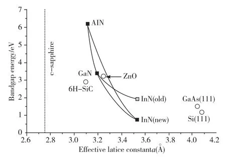
图1 Ⅲ-氮化物的带隙能和晶格常数(实心矩形)。异质外延Ⅲ-氮化物作基板的有效晶格常数(空心圆圈)Fig.1 Bandgaps energy and lattice constants of Ⅲ-nitrides (solid rectangles). Effective lattice constants considered as substrates for hetero-epitaxy of Ⅲ-nitrides (hollow circles).
目前,InN已被证明是一个窄带隙半导体材料,在低温带隙能为0.65eV,室温下约为0.7eV[17-22]。这一观察结果具有很大的价值,因为这使得Ⅲ-氮化物和它们的三元、四元合金带隙宽度范围不仅仅是1.9e~6.2eV,而是扩大至0.65e~6.2eV,覆盖了从红外到深紫外全部区域,使得Ⅲ-族氮化物在光电器件中的应用比以前更具吸引力。例如,先前以Ⅲ-族氮化物为基础的发光二极管(LED),通常仅仅活跃在绿色、蓝色和紫外范围内,现在可以一直延伸到红色范围内。这表明,Ⅲ-族氮化物基LED可以取代其它诸如GaAs基材料的LED。因此,仅基于Ⅲ-族氮化物的LED就足以形成大屏幕显示器和白光照明,那么GaN基蓝光和绿色LED与GaAs基LED的组合就不再是唯一的选择。由于InN狭窄的带隙,Ⅲ-族氮化物基的LD也可以延伸到红外范围内,因而可广泛应用于光通信。此外,InN和GaN合金的发射谱线几乎可以匹配整个太阳光谱。因此,我们不仅可以通过设计最佳的光学带隙比例(1.1/1.7eV)构制成双层电池[23],而且可以多层组合制成优异的叠层电池。InAlN的带隙能同样覆盖0.65~6.2eV范围,同样能够制成高效率的太阳能电池。
宽带隙的GaN、AlN和它们的合金在高温度和高功率电子器件的应用上有很大的潜能。相比较GaAs、Si和Ge,由于禁带宽度大,Ⅲ-族氮化物具有较大热导率,这对器件和设备冷却系统非常有益。GaN、AlN和它们的合金的的击穿场强也高于Si和GaAs。GaN还具有非常出色的电子输送性质(室温下一个电子的迁移速率为1300cm2·v-1)和高饱和电子漂移速度(室温下3×107cm·s-1)。GaN异质结场效应晶体管(HFETs)材料和一系列的单极型和双极型晶体管电子器件优异特性是其实用化最引人注目的例子[24]。InN已被预测是Ⅲ-族氮化物中电子有效质量最低的氮化物,并拥有最快的迁移速率(室温下约4400 cm2·V-1·s-1)。室温下InN具有非常高的漂移速度峰值(4.2×107cm·s-1)。这说明InN的电子输送能力比GaN还要好,已经预测,0.1μm的InN基场效应管,截止频率在1Hz以上。因此,InN是制造如高速FETs等电子设备的优良半导体材料。
2 Ⅲ-族氮化物的掺杂
掺杂是对包括氮化物在内的所有半导体的一个重要研究方向。未掺杂的GaN属于N-型材料,具有最低的电子浓度(1016cm-3)。降低电子浓度一直是研究氮化物以来面临的一个难题。20世纪80年代后期使用Mg掺杂p型GaN的研究使得氮化物获得快速发展。
2.1 N-型掺杂
硅掺杂和锗掺杂都能有效地得到高电子浓度的N型Ⅲ-族氮化物。由于Si在Ⅲ-族氮化物中溶解度更高,所以Si掺杂使用的更加广泛。硅和锗在GaN中取代Ga产生浅施主能级。Jain等得出结论,通过电气方法确定的Si的活化能在12~17meV的范围内。据报道[25]通过MBE生长Si掺杂的GaN的电子浓度在1020cm-3以上。Hageman等[26]报道掺Ge的GaN电子浓度高达4×1020cm-3。除了硅和锗外,硒也常用于N-型掺杂。
2.2 P-型掺杂
P型掺杂的GaN一直是一个难以攻克的难题,研究者已经进行了大量工作对P型掺杂的GaN及其合金的研究。20世纪80年代后期Amano等[27-28]利用MOVPE技术用Mg作掺杂剂首次获得P型GaN。他们发现,掺杂Mg的GaN可以用低能电子束照射反转为P型GaN,这可能与Nakamura等人[29-30]报告的加热GaN层具有相同的效果。Nakamura发现,在真空或氮气气氛下经热处理也能成功获得P型材料。并且,为了激活Mg,热退火处理对于MOVPE法生长GaN是不可或缺的。G☒tz等[31]报告说,通过热退火处理后活化的Mg杂质使GaN电阻率下降了超过6个数量级。
分子束外延法生长的Mg-掺杂GaN的性能与MOVPE生长的GaN不同,没有必要经过热退火处理,因为热退火处理甚至都不改变掺杂的GaN膜的电特性[32]。Mg的掺入取决于GaN的生长条件。Berishev等[33]报道,在富N和较低生长温度条件下Mg更容易融入到GaN。在MBE生长GaN中,极性对掺杂效率有较大的影响。相比N-极性表面,Mg更容易掺入Ga-极性的GaN中。Ptak报告说[34],通过二次离子质谱法已经检验到在一定条件下能使高达30倍以上的Mg掺入到Ga的极层。
其他P型掺杂物包括C、Be、Cd、Ca。理论上Be是P型掺杂的一个非常理想的候选金属,因为处在纤锌矿氮化镓的Ga晶格位点上时其电离能达到60 meV[35-36],Nakano等[37]报道当Be掺杂的活化能为231meV时可获得轻微的P型导电性。C通常被用来置换GaN中的N原子变成一个电子接受体。研究已经表明在Ga和N浓度较高的生长条件下C可以很容易地被掺入,当C的浓度在1017~1019cm-3之间时没有观察到结构质量被破坏[38]。Schurman等[39]报道MOMBE生长掺杂碳P型氮化镓,最大的空穴浓度为3×1017cm-3,而流动性约为100cm2·V-1·s-1。Mensching等[40]报道用MBE生长法在Ca植入的GaN中发现了P型载流子的存在。
2.3 其他掺杂
由于光通信用1.55μm区域的重要性,很多研究者已经花了大量精力研究Er掺杂Ⅲ-氮化物。从掺铒GaN和AlN的PL光谱中观察1.55μm排放[41]。在这个波长,Qiu等[42]演示电致发光设备(ELD)的室温操作。掺铒GaN的光致发光和电致发光在537nm和558 nm也出现了绿光发射[43]。Eu掺杂GaN,在621 nm有一条狭窄的红色发射线,在543~663 nm范围间有几个较弱的发射线[45]。Steckl等[46]报道由固态源分子束外延生长法生长的各种稀土元素掺杂GaN薄膜的发射光能覆盖整个可见光谱。原位稀土掺杂的氮化镓发光二极管,基于铒掺杂的规律能产生绿光,基于镨掺杂的规律能产生红光[47-49]。
由于电荷载流子的自旋,强磁性半导体可能会引发新一代微电子器件热潮,这使得其近年来备受关注[50]。 因为Ⅲ-族氮化物的居里温度预测在室温以上,所以Ⅲ-族氮化物是非常合适的候选材料[51]。在铁磁Ⅲ-族氮化物之中研究最多的是Mn掺杂GaN。Sasaki等[52]报道了用MBE在C-蓝宝石上生长Mn掺杂GaN薄膜,其居里温度高达940K。磁化场和温度的关系呈现铁磁相和顺磁相共存。Kim等[53]报道Mn和Mg的共掺杂可以提高GaN的磁性。Graf等[54]报道了MBE生长Mn掺杂的铁磁性氮化铝。 在Fe掺杂GaN中发现低于100K的铁磁行为。EXAFS数据表明,约为1019cm-3浓度的Fe取代Ga的位置[55]。MBE展现了生长高品质掺杂锰或其他元素的铁磁Ⅲ族氮化物的优势。
3 Ⅲ-氮化合物合金
3.1 InGaN
InGaN和InGaN量子肼是LED和LD有源区的关键结构。In1-xGaxN的能带隙可以表示为:

其中Eg(InN)和Eg(GaN)分别是InN和GaN的带隙能,b是In1-xGaxN的弯曲系数。
目前,InN的能带隙能被重新证明是0.7eV左右,Wu等[56]报道了通过拟合MBE生长的纤维锌矿In1-xGaxN(0≤x≤0.5),结果得出能带隙的弯曲指数为1.43eV,因此,方程(1)可直接表示为:

六方和立方氮化铟镓都已通过MBE成功生长。生长InGaN通常需要一个GaN和AlN缓冲层或者模板。六方晶系InGaN的生长也常受极性的影响。Shen等[57]报道在极性GaN模板上通过MBE生长InGaN薄膜,他们发现在Ga极性GaN模板生长的InGaN质量优于N极性生长的InGaN。Chen等[58]报道当In作为表面活性剂沉积在N-极性GaN表面时,In原子对平滑到粗化生长的过渡只有一个很小的影响,沉积在Ga极性氮化镓表面时对平滑生长起着很大的作用。已经有报道[59-60]在砷化镓(GaAs)和3C-SiC上生长立方InGaN层。在InGaN的生长过程中In的分布是不均匀的,这种非均匀分布大大影响PL性能,这就是所谓的独立定位效应[61]。Wang Yadong等[62]通过控制生长时间合成了一系列类型的InGaN纳米结构材料(图2)。
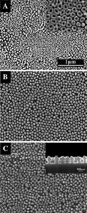
(a)纳米环(插图为放大尺寸图);(b)纳米点;(c)纳米箭(插图为剖面图)图2 InGaN纳米结构SEM图(a) nanorings (inset shows the larger magnitude); (b) nanodots; and (c) nanoarrows (inset shows the cross-sectional view)Fig 2 . SEM images of InGaN nanostructures
3.2 InAlN
相比于InGaN,AlGaN的研究报道相对较少,InAlN吸引人的特点是从0.65~6.2eV宽的带隙以及In0.17Al0.83N与GaN高的的晶格匹配。与InGaN类似,In1-xAlxN的能带隙可以表示为:

InAlN的弯曲系数报道的有很多,如2.5eV、2.74eV、1.32eV和2.38eV。He Hong等[63]研究了通过磁控溅射法制备的In富裕InxAl1-xN薄膜的透射光谱和吸收系数(图3)。InAlN通常生长在GaN或AlN层模板上。Higashiwaki等人[64]报道了InAlN薄膜在InN层上的生长。最近,Gačević ☒等[65]研究了InAlN单层组成,应变和表面形貌,与生长温度的函数关系,并构建了一个全面的InGaN生长图。
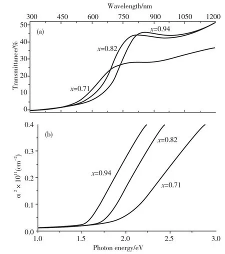
a)透射光谱;(b)平方吸收系数α2图3 不同浓度InxAl1-xN薄膜的光学性质(a) transmittance spectra (b) squared absorption coefficient α2Fig. 3. Optical properties of InxAl1-xN films with different In content
3.3 AlGaN
AlGaN已被人们深入的研究并广泛应用于LDs的阻挡层和电子设备。AlGaN的带隙能可以表示为:

Lee等[66]将自己得到的AlGaN弯曲系数与其他人报道的弯曲系数做了比较,发现所测带隙与外延生长的AlxGa11-xN之间有相关性,在温度大于800℃下直接核化或缓冲生长在蓝宝石衬底上的InGaN,通常有一个较大的弯曲系数(b>+1.3eV)。若最初使用低温缓冲生长在蓝宝石衬底上,然后在高温下生长,会导致一个较弱的弯曲系数(b<+1.3eV)。lliopoulos等[67]报道了AlGaN薄膜生长动力学。他们发现,Al的掺入概率在整个温度范围是统一的。他们研究了富N和富Ⅲ基团的生长情况。另一方面,只有在富N条件下,Ga的掺入概率是恒定的(小于1)。在这种情况下Ga的掺入概率取决于薄膜表面Ga的解吸与活化能,在富金属情况下,掺杂的Al和Ga原子之间存在相互竞争,并且掺杂的Ga单独由没有被Al消耗完的有效氮流所控制。He Chengyu等[68]通过化学气相沉积法成功的制备了整个组成范围的AlxGa1-xN 合金纳米锥,通过电子显微镜,X射线衍射,能量色散型X射线光谱仪,和选区电子衍射等表征揭示了所制备的纤锌矿型AlxGa1-xN纳米锥组成分布均匀,具有单晶结构,并且沿c轴优先生长(图4),这为进一步发展先进的纳米光电设备提供了新的可能性。
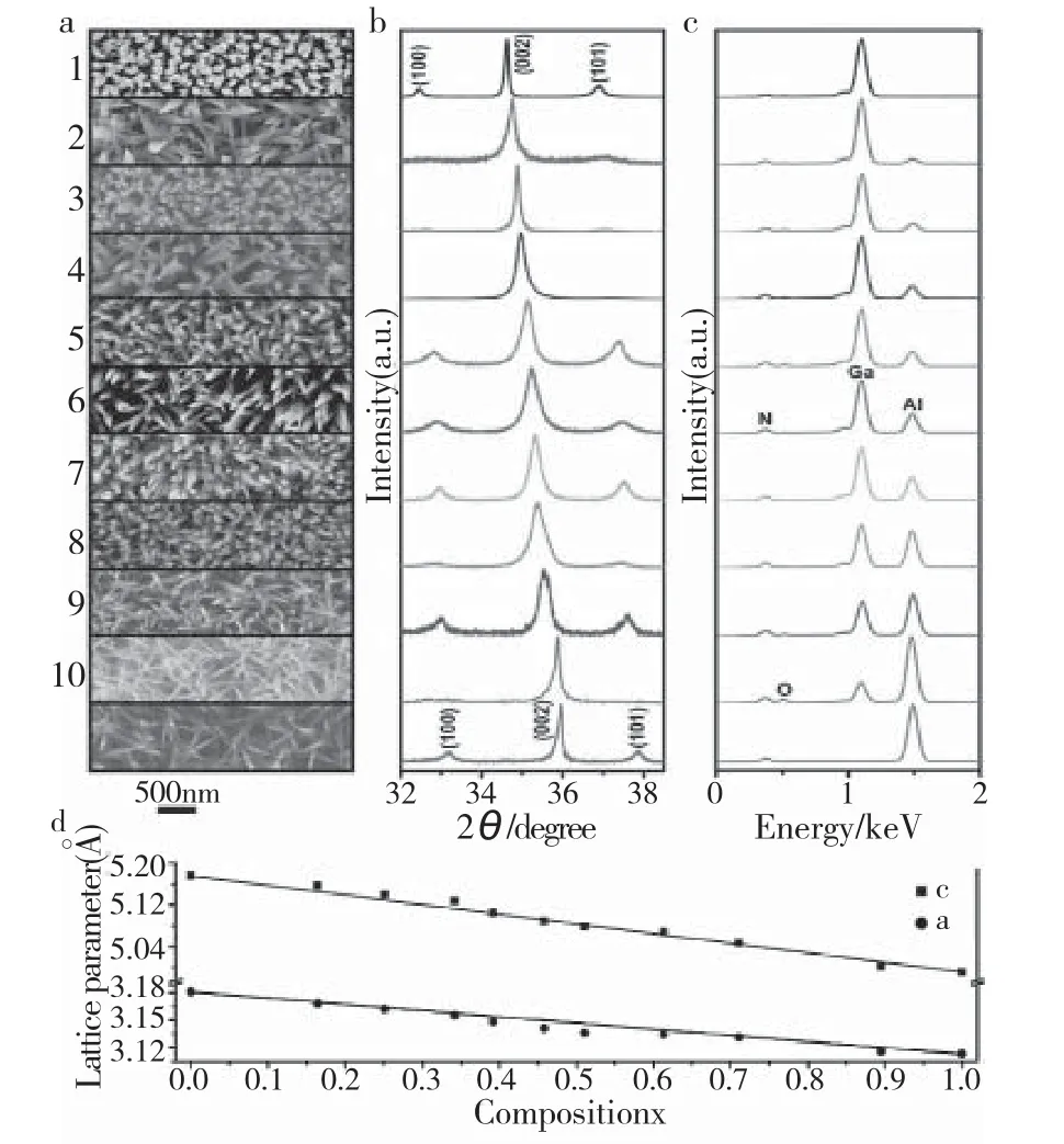
a)SEM图;(b)特征峰为 (100),(002),(101)的XRD谱图;(c)有明显元素信号的SEM-EDS光谱;(d)AlxGa1-xN的晶格常数c和a随着x的变化曲线图4 1号到11号,随着铝含量增加AlxGa1-xN的SEM、XRD以及EDS表征谱图(a) SEM images. (b) XRD patterns with the characteristic peaks of (100), (002), and (101). (c) SEM-EDS spectra with marked elemental signals. (d) The curve of lattice parameters c and a of AlxGa1-xN with x changedFigure 4 SEM, XRD and EDS characterizations on a sequence of AlxGa1-xN products with increasing Al content from no.1 to no.11.
由于能够作为包覆层应用在LDs中,掺杂的AlGaN具有很高的价值。Si常常被用作一种N型掺杂物,Mg常常被用作一种P型掺杂物,当铝的浓度较小时,Si掺杂效率很高,一个浓度为1019cm-3的Si,在室温下足以使准金属导电[69]。对于更高的Al浓度,由于电子迁移率的降解和Si施主能级带隙的移位,导电性会急剧降低。P型掺杂十分困难。由于Al掺入会引起受主能级移位,关于P型AlGaN研究报道很少。Stutzmann等[69]通过使用热电势观察过掺杂Mg的AlGaN的P型电导系数。
6 结语
Ⅲ-族氮化物带隙能从红光波段一直覆盖到紫外波段,不仅是制作红、黄、绿,特别是蓝光发光二极管(LED)和激光二极管(LD)、大功率晶体管的最佳候选材料,而且由于其在紫外光检测器、太阳能光伏、场效应晶体管等方面同样具有广阔的应用前景,近年来,Ⅲ-族氮化物引起了科学工作者的极大兴趣,并取得了重大的进展。单分散、高密度、无缺陷、排列有序Ⅲ-族氮化物材料制备,均一尺寸Ⅲ-族氮化物量子点掺杂于透明玻璃和陶瓷等基质内的可控生长,大的带隙发射材料的合成具有重要的学术意义和广阔的应用前景,都将是未来半导体材料领域具有挑战性的研究课题。经过各国研究者的不断努力,相信Ⅲ-族氮化物半导体材料和器件将会在更多的领域实现实用化。
[1] Bernardini F. Spontaneous and piezoelectric polarization:Basic theory vs. practical recipes[M].Wiley-VCH, Weinheim, 2007.
[2] Ambacher O. Growth and applications of group Ⅲ-nitrides[J]. Journal of Physics D: Applied Physics, 1998, 31(20): 2653.
[3] Morkoc H. Nitride semiconductors and devices[M]. Springer Verlag, 1999.
[4] Nakamura S, Pearton S, Fasol G. The blue laser diode: the complete story[M]. Springer, 2000.
[5] Pearton S J, Kuo C. GaN and related materials for device applications[J]. MRS Bulletin, 1997,22(2): 17-21.
[6] GroupⅢ nitride semiconductor compounds: physics and applications[M]. Clarendon, 1998.
[7] Pankove J I, Moustakas T D, Willardson R K. Gallium Nitride (GaN) I[M]. Academic Press, 1998.
[8] Jain S C, Willander M, Narayan J, et al.Ⅲ-nitrides: Growth, characterization, and properties[J].Journal of Applied Physics, 2000, 87(3): 965-1006.
[9] Pearton S J, Ren F. GaN electronics[J]. Advanced Materials, 2000, 12(21): 1571-1580.
[10] Morko☒ H, Carlo A D, Cingolani R. GaN-based modulationdoped FETs and UV detectors[J].Solid-State Electronics, 2002, 46(2): 157-202.
[11] Pearton S J, Zolper J C, Shul R J, et al. GaN: Processing, defects, and devices[J]. Journal of Applied Physics, 1999, 86(1): 1-78.
[12] Deger C, Born E, Angerer H, et al. Sound velocity of AlGaN thin films obtained by surface acoustic-wave measurements[J]. Applied physics letters, 1998, 72: 2400.
[13] VurgaftmanI,Meyer JR. Band parameters for nitrogencontaining semiconductors[J].Journal of Applied Physics, 2003, 94(6): 3675-3696.
[14] Strite S, Morkoc H. GaN, AlN, and InN: a review[J]. Journal of Vacuum Science & Technology B: Microelectronics and Nanometer Structures, 1992, 10(4): 1237-1266.
[15] Nakamura S, Senoh M, MukaiT.P-GaN/N-InGaN/N-GaN double-heterostructure blue-light-emitting diodes[J]. Japanese Journal of Applied Physics Part 2 Letters, 1993(32): L8.
[16] Nakamura S, Senoh M, Nagahama S,et al.Violet InGaN/ GaN/AlGaN-based laser diodes operable at 50 C with a fundamental transverse mode[J]. Japanese journal of applied physics, 1999(38): L226-L229.
[17] Xu K, Yoshikawa A. Effects of film polarities on InN growth by molecular-beam epitaxy[J]. Applied physics letters, 2003, 83(2): 251-253.
[18] Wu J, Walukiewicz W. Band gaps of InN and groupⅢnitride alloys[J]. Superlattices and Microstructures, 2003, 34(1): 63-75.
[19] Davydov V Y, Klochikhin A A, Seisyan R P, et al. Absorption and emission of hexagonal InN.Evidence of narrow fundamental band gap[J]. physica status solidi (b), 2002, 229(3): r1-r3.
[20] J. Wu, W. Walukiewicz, K.M. Yu, J.W. ArgerⅢ , E.E. Haller, H. Lu, W.J. Schaff, Y. Saito,Y. Nanishi, Appl. Phys. Lett., 2002(80): 3967.
[21] Bhuiyan A G, Hashimoto A, Yamamoto A. Indium nitride (InN): A review on growth,characterization, and properties[J]. Journal of Applied Physics, 2003, 94(5):2779-2808.
[22] Nanishi Y, Saito Y, Yamaguchi T. RF-molecular beam epitaxy growth and properties of InN and related alloys[J]. Japanese journal of applied physics, 2003, 42(part 1):2549-2559.
[23] Rault F K, Zahedi A. Ideal quantum well solar cell designs[J]. Physica E: Low-dimensional Systems and Nanostructures, 2004, 21(1): 61-70.
[24] Nakajima A, Dhyani M H, Narayanan E M S, et al. GaN based Super HFETs over 700V using the polarization junction concept[C]//Power Semiconductor Devices and ICs (ISPSD), 2011 IEEE 23rd International Symposium on. IEEE, 2011: 280-283.
[25] Ng H M, Doppalapudi D, Korakakis D, et al. MBE growth and doping of Ⅲ-V nitrides[J]. Journal of crystal growth, 1998(189): 349-353.
[26] Hageman P R, Schaff W J, Janinski J, et al. n-type doping of wurtzite GaN with germanium grown with plasmaassisted molecular beam epitaxy[J]. Journal of crystal growth, 2004, 267(1): 123-128.
[27] Amano H, Sawaki N, Akasaki I, et al. Metalorganic vapor phase epitaxial growth of a high quality GaN film using an AlN buffer layer[J]. Applied Physics Letters, 1986(48):353.
[28] Amano H, Akasaki I, Kozawa T, et al. Electron beam effects on blue luminescence of zinc-doped GaN[J]. Journal of Luminescence, 1988(40):121-122.
[29] Nakamura S, Mukai T, Senoh M, et al. Thermal annealing effects on p-type Mg-doped GaN films[J]. Jpn. J. Appl. Phys., 1992, 31(2B): L139-L142.
[30] Nakamura S, Mukai T, Senoh M, et al. Thermal annealing effects on p-type Mg-doped GaN films[J]. Jpn. J. Appl. Phys., 1992, 31(2B): L139-L142.
[31] Gotz W, Johnson N M, Walker J, et al. Activation of acceptors in Mg-doped GaN grown by metal organic chemical vapor deposition[J]. Applied physics letters, 1996, 68(5): 667-669.
[32] Kim W, Salvador A, Botchkarev A E, et al. Mg-doped p-type GaN grown by reactive molecular beam epitaxy[J]. Applied physics letters, 1996, 69(4): 559-561.
[33] Berishev I, Kim E, Fartassi A, et al. Mg doping studies of electron cyclotron resonance molecular beam epitaxy of GaN thin films[J]. Journal of Vacuum Science & Technology A:Vacuum, Surfaces, and Films, 1999, 17(4):2166-2169.
[34] Ptak A J, Myers T H, Romano L T, et al. Magnesium incorporation in GaN grown by molecular-beam epitaxy[J]. Applied Physics Letters, 2001, 78(3): 285-287.
[35] Bernardini F, Fiorentini V, Bosin A. Theoretical evidence for efficient p-type doping of GaN using beryllium[J]. Applied physics letters, 1997, 70(22): 2990-2992.
[36] Neugebauer J, Van de Walle C G. Chemical trends for acceptor impurities in GaN[J]. Journal of applied physics, 1999, 85(5): 3003-3005.
[37] Nakano Y, Jimbo T. Electrical characterization of acceptor levels in Be-implanted GaN[J].Applied physics letters, 2002, 81(21): 3990-3992.
[38] Green D S, Mishra U K, Speck J S. Carbon doping of GaNwith CBr4 in radio-frequency plasma-assisted molecular beam epitaxy[J]. Journal of applied physics, 2004, 95(12):8456-8462.
[39] Schurman M J, Slagaj T, Tran C, et al. Reproducibility of GaN and InGaN films grown in a multi-wafer rotating-disc reactor[J]. Materials Science and Engineering: B, 1997, 43(1): 222-227.
[40] Mensching B, Liu C, Rauschenbach B, et al. Characterization of Ca and C implanted GaN[J].Materials Science and Engineering: B, 1997, 50(1): 105-108.
[41] V. Dierolf, C. Sandmann, J. Zavada, P. Chow, B. Hertog, J. Appl. Phys.,2004(95): 5464.
[42] Qiu C H, Leksono M W, Pankove J I, et al. Cathodoluminescence study of erbium and oxygen coimplanted gallium nitride thin films on sapphire substrates[J]. Applied physics letters, 1995, 66(5): 562-564.
[43] Lee D S, Steckl A J. Lateral color integration on rare-earthdoped GaN electroluminescent thin films[J]. Applied physics letters, 2002, 80(11): 1888-1890.
[44] Heikenfeld J, Garter M, Lee D S, et al. Red light emission by photoluminescence and electroluminescence from Eudoped GaN[J]. Applied physics letters, 1999, 75(9): 1189-1191.
[45] Steckl A J, Heikenfeld J, Garter M, et al. Rare earth doped gallium nitride-light emission from ultraviolet to infrared[J]. Compound Semicond, 2000, 6(1):48-50.
[46] Steckl A J, Garter M, Birkhahn R, et al. Green electroluminescence from Er-doped GaN Schottky barrier diodes[J]. Applied physics letters, 1998, 73(17): 2450-2452.
[47] Garter M, Scofield J, Birkhahn R, et al. Visible and infrared rare-earth-activated electroluminescence from indium tin oxide Schottky diodes to GaN: Er on Si[J]. Applied physics letters, 1999, 74(2): 182-184.
[48] Birkhahn R, Garter M, Steckl A J. Red light emission by photoluminescence and electroluminescence from Prdoped GaN on Si substrates[J]. Applied physics letters, 1999, 74(15): 2161-2163.
[49] Pearton S J, Abernathy C R, Overberg M E, et al. Wide band gap ferromagnetic semiconductors and oxides[J]. Journal of Applied Physics, 2003, 93(1): 1-13.
[50] Dietl T, Ohno H,Matsukura F, et al. Zener model description of ferromagnetism in zinc-blende magnetic semiconductors[J].Science, 2000, 287(54/55): 1019-1022.
[51] Sasaki T, Sonoda S,Yamamoto Y, et al. Magnetic and transport characteristics on high Curie temperature ferromagnet of Mn-doped GaN[J].Journal of applied physics, 2002, 91(10): 7911-7913.
[52] Kim K H, Lee K J, Kim D J, et al. Improvement of magnetic property of GaMnN by codoping of Mg[J]. Journal of applied physics,2003, 93(10): 6793-6795.
[53] Graf T, Gjukic M, Hermann M, et al. Spin resonance investigations of Mn2+in wurtzite GaN and AlN films[J]. Physical Review B,2003, 67(16): 165215.
[54] Akinaga H, Nemeth S, De Boeck J, et al. Growth and characterization of low-temperature grown GaN with high Fe doping[J]. Applied Physics Letters, 2000, 77(26): 4377-4379.
[55] Wu J, Walukiewicz W, Yu K M, et al. Small band gap bowing in InGaN alloys[J]. Applied Physics Letters,2002(80): 4741.
[56] Shen X Q, Ide T, Shimizu M, et al. Growth and characterizations of InGaN on N-and Ga-polarity GaN grown by plasma-assisted molecular-beam epitaxy[J]. Journal of crystal growth, 2002(237): 1148-1152.
[57] Chen H, Feenstra R M, Northrup J E, et al. Surface structures and growth kinetics of InGaN (0001) grown by molecular beam epitaxy[J]. Journal of Vacuum Science & Technology B:Microelectronics and Nanometer Structures, 2000, 18(4): 2284-2289.
[58] Kitamura T, Cho S H, Ishida Y, et al. Growth and characterization of cubic InGaN epilayers on 3C-SiC by RF MBE[J]. Journal of crystal growth, 2001(227): 471-475.
[59] Brandt O, Müllhaüser J R, Trampert A, et al. Properties of cubic (In, Ga) N grown by molecular beam epitaxy[J]. Materials Science and Engineering: B, 1999, 59(1): 73-79. [60] Naranjo F B, Calle F, Calleja E, et al. Strong localization in InGaN layers with high In content grown by molecularbeam epitaxy[J]. Applied physics letters, 2002, 80(2): 231-233.
[61] Wang Y, Zang K, Chua S, et al. High-density arrays of InGaN nanorings, nanodots, and nanoarrows fabricated by a template-assisted approach[J]. The Journal of Physical Chemistry B,2006,110(23):11081-11087.
[62] He H, Cao Y, Fu R, et al. Band gap energy and bowing parameter of In-rich InAlN films grown by magnetron sputtering[J]. Applied Surface Science,2010, 256(6): 1812-1816.
[63] Higashiwaki M, Matsui T. Plasma-assisted MBE growth of InN films and InAlN/InN heterostructures[J]. Journal of crystal growth, 2003, 251(1): 494-498.
[64] Gačević ☒, Gómez V J, Lepetit N G, et al. A comprehensive diagram to grow (0001) InGaN alloys by molecular beam epitaxy[J]. Journal of Crystal Growth, 2013(364): 123-127.
[65] Lee S R, Wright A F, Crawford M H, et al. The band-gap bowing of AlxGa1-xN alloys[J].Applied physics letters, 1999, 74(22): 3344-3346.
[66] Iliopoulos E, Moustakas T D. Growth kinetics of AlGaN films by plasma-assisted molecular-beam epitaxy[J]. Applied physics letters, 2002, 81(2): 295-297.
[67] He C, Wu Q, Wang X, et al. Growth and Characterization of Ternary AlGaN Alloy Nanocones across the Entire Composition Range[J]. ACS nano, 2011, 5(2): 1291-1296.
[68] Stutzmann M, Ambacher O,Cros A, et al. Properties and applications of MBE grown AlGaN[J]. Materials Science and Engineering: B, 1997, 50(1): 212-218.
Research Progress on Ⅲ-Nitride Semiconductors
HAN Bo, LI Zhong-yu, LAN Yun-jun
(College of Chemistry and Material Engineering, Wenzhou 325035, China)
Ⅲ -nitri de semiconductor materials had received the scientific researchers’ attention and obtained dramatically development in recent years. In this paper, the development of Ⅲ -nitride materials and devices were introduced. The research situation on doping of Ⅲ-nitride and alloys of Ⅲ-nitride were reviewed. Finally, potential application of Ⅲ-nitride in the future was brief y predict.
Ⅲ-nitride; semiconductor; research progress
文献标识码:A
1671-9905(2015)03-00 -
韩波(1988),男,硕士,内蒙古赤峰市人,E-mail:18367803373@163.com
2015-01-15