Digital synthesis of programmable photonic integrated circuits
2022-02-24JuanZhang张娟ZhengyongJi计正勇YipengDing丁一鹏andYangWang王阳
Juan Zhang(张娟) Zhengyong Ji(计正勇) Yipeng Ding(丁一鹏) and Yang Wang(王阳)
1Key Laboratory of Specialty Fiber Optics and Optical Access Networks,School of Communication and Information Engineering,Shanghai University,Shanghai 200444,China2School of Physical Science and Electronics,Central South University,Changsha 410012,China3Shanghai Institute of Optics and Fine Mechanics,Chinese Academy of Sciences,Shanghai 201800,China
Programmable photonic waveguide meshes can be programmed into many different circuit topologies and thereby provide a variety of functions. Due to the complexity of the signal routing in a general mesh, a particular synthesis algorithm often only accounts for a specific function with a specific cell configuration. In this paper, we try to synthesize the programmable waveguide mesh to support multiple configurations with a more general digital signal processing platform.To show the feasibility of this technique, photonic waveguide meshes in different configurations (square, triangular and hexagonal meshes)are designed to realize optical signal interleaving with arbitrary duty cycles. The digital signal processing(DSP)approach offers an effective pathway for the establishment of a general design platform for the software-defined programmable photonic integrated circuits. The use of well-developed DSP techniques and algorithms establishes a link between optical and electrical signals and makes it convenient to realize the computer-aided design of optics–electronics hybrid systems.
Keywords: photonic integrated circuit,digital signal processing,Z-transform
1. Introduction
Recent developments in nanophotonics have enabled increasing research on programmable photonic integrated circuits (PPICs) for various applications in communication, artificial neural networks, and quantum information technologies.[1–14]In PPICs, optical signal processing is performed in a linear optical core consisting of a Mach–Zehnder interferometer (MZI) waveguide mesh, where the topology and connectivity define the possible implementable functionalities. Different devices or subsystems can be demonstrated in the single hardware platform by programming its control signals. Similar to the field-programmable gate arrays (FPGAs) in electronics, the versatile architecture and multifunctionality of PPICs will enable us to considerably reduce the required time and cost to design, fabricate, and test different photonic chips.
The programming or reconfiguration of photonic waveguide meshes is realized with tunable optical building blocks in MZIs,such as couplers/beam splitters and phase shifters,normally controlled by electronics. The programmable meshes can be divided into two major categories according to the signal routing approaches. One is the forward-propagation configuration.[4,8,16]Linear optical transformations are implemented by the one-way propagation from a set of input ports to a set of output ports.[3,15]The other is the reverse-feedback configuration.[18–20]Waveguides are connected in loops that can implement differential delay lines, ring resonators, and optical feedback circuits, enabling applications such as finite/infinite impulse response(FIR/IIR)multiport filters.[6,17]In fact, both forward- and reverse-feedback programmable configurations can be realized in a general MZI mesh by selecting appropriate structural parameters of tunable optical building blocks,regardless of the shape of the mesh cell(such as square-,triangular-,and hexagonal-shaped meshes).
Due to the complexity of the signal routing in a general mesh,a particular synthesis algorithm often only accounts for a specific function (such as an FIR filter) with a specific cell configuration. It is a great challenge to synthesize the programmable waveguide mesh that supports multiple configurations with a more general design platform.[21]
From another point of view, in the FPGA-like photonic processor, the reconfigurable optical core (MZI mesh)is integrated with some electrical elements and subsystems,such as control electronics, an input/output electronics interface, and electro-optical/photoelectric converters to support software programming. Although the all-photonic system is the ultimate target, optical networks will require the cointegration of electronics and photonics over a long period of time,such as the combination of complementary metal-oxidesemiconductor(CMOS)electronics and silicon photonics.[22]Heterogeneous integration of these technologies will eventually be limited by totally different design approaches.
Fortunately, both electric and optical systems can be described using the theory of digital signal processing (DSP).Although DSP is often considered an important branch of electronics and telecommunication engineering,many popular optical devices, especially in optical communications, could be represented with a digital filter model,as described in our previous work.[23–27]The use of well-developed DSP techniques and algorithms to design these optical devices is not only a wise use of existing technology but also establishes a link between optical and electrical signals.[28,29]Furthermore,extensive DSP simulation applications make it convenient to realize software-programming and computer-aided design of optics–electronics hybrid systems.
In this paper, the digital signal model of the optical core of the PPIC is proposed for the first time. To showcase the potential of this technique, the DSP algorithm is used to design optical interleavers with tunable duty cycles. The effect of the shape of the mesh cell, and the design and fabrication errors of the tunable basic unit (TBU) on the performance of interleaving are discussed in detail. The DSP approach offers an effective pathway for the establishment of a general design platform for software-defined PPICs.
2. DSP model of integrated waveguide meshes
The integrated waveguide meshes are composed of unitary TBUs, which are interconnected to create cells with different shapes (such as square, triangular, and hexagonal configurations). Figure 1(a)shows a typical square-shaped mesh with 9 cells.[18]As shown in Fig.1(b),each TBU is composed of two 3-dB couplers and two parallel waveguides with upper and lower phase shifters,φuandφl, respectively. By controlling the phase shift, any TBU in the mesh can operate either as a directional coupler or an optical cross-bar switch, thus providing independent amplitude- and phase-controlled optical routing,as shown in Fig.1(c). The ideal transfer matrix of a TBU can be expressed as

Fig.1. The layout of a 9-cell square mesh and a zoom of an interconnection node.(b)The structure of a TBU with 1×basic unit length(BUL).(c)Signal flow for different functions of a TBU.

Fig. 2. Square (left), hexagonal (middle), and triangular (right) mesh configurations to implement (a) a single-stage ORR, (b) a coupled multi-stage ORR,(c)a cascaded multi-stage ORR,and(d)an MZI.In and out are the input and output ports of light,respectively.

whereθ=(φu−φl)/2 andΔ=(φu+φl)/2.
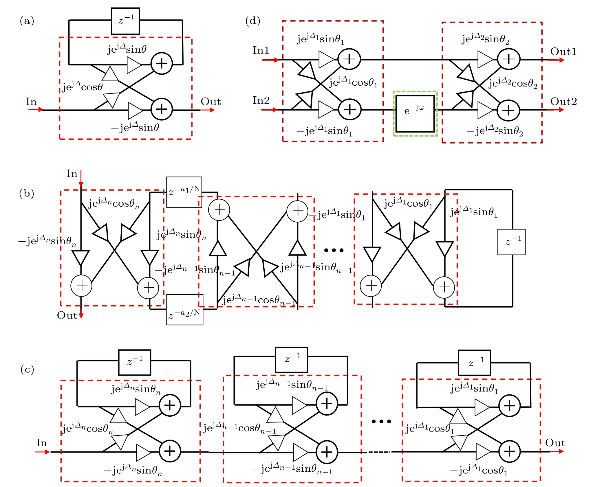
Fig.3. The DSP model of the mesh configurations shown in(a)Fig.2(a),(b)Fig.2(b),(c)Fig.2(c),and(d)Fig.2(d).
The meshes can be reconfigured from MZIs to optical ring resonators(ORRs)with the feedback response. Figure 2 shows the square, hexagonal, and triangular mesh configurations corresponding to a single-stage ORR, a coupled multistage ORR, a cascaded multi-stage ORR, and a typical MZI,respectively. The direction of light propagation in the ORRs and MZIs is indicated by arrows in the figures.
According to the transfer characteristics of the basic unit shown in Eq. (1), the DSP model of these mesh configurations can be presented in Fig. 3, respectively. The Z transformation operator, which denotes the signal delay, is related to the structural parameters of the optical systems byz−1=e−j·2π·ne·N·BUL/λ,whereneis the effective refractive index of the waveguide,BUL is the length of a TBU,andNis the number of TBUs in the ORR(for one round trip). For example, in the configuration shown in Figs.2(a)and 3(a),N=4,6,and 3 for square,hexagonal,and triangular meshes,respectively. In Fig.3(d),φis the phase delay induced by the length difference in the two arms of an MZI.For square,hexagonal,and triangular mesh configurations, the length differences in the two armsΔLare 4×BUL,6×BUL,and 3×BUL,respectively.
From Fig. 3(a), the transfer function of the single-stage ORR can be expressed as

whereis the conjugate ofρr. The transfer function of the coupled multi-stage ORR can be derived from Fig.3(b)as follows:

For the simplest multi-stage structure composed of two ring resonators, its transfer function can be deduced from Eq. (3)as

For the cascaded multi-stage ORR,its transfer function can be written as

From Fig.3(d),we can obtain the transfer function of the MZI as

whereθ1,Δ1, andθ2,Δ2are the parameters of the tunable coupler at the input and output ports,respectively. The phase delayφ=2π·ne·ΔL/λ.
From the combination of different configurations, the mesh can be reconfigured to realize different optical functions.For a mesh configuration composed of an MZI with cascaded single-stage ORR and multi-stage ORR in the upper and lower arms,its transfer function can be expressed as

whereHup(z) andHlow(z) are the transfer functions of ring resonators located in the upper and lower arms and can be obtained from Eqs.(2)and(3)(or Eq.(5)),respectively.
3. Design principle of integrated waveguide meshes
Filtering is one of the most important and complicated DSP applications. It includes complex matrix operations,which are often concerned with optics and photonics fields.Computer-based DSP platforms(such as Matlab DSP toolbox)provide various algorithms and design tools for streaming signal processing to achieve designed filtering and routing functions. Taking filters as examples,the design principles of integrated waveguide meshes are presented.
The optimum bandpass filters, which include the Butterworth, Chebyshev, and elliptic filters, are very important for signal processing to meet desired bandpass and stopband requirements. Elliptical filters have equal ripples in both the passband and stopband and no other filters with equal order can obtain a faster transition in gain between the passband and stopband.[25]Therefore,the design method for elliptical filters is adopted. The transfer function of the synthesized filter can be expressed as[29]

whereP(z)andD(z)are two polynomials ofzwith real coefficients,in whichP(z)has even symmetry. Equation(10)can be decomposed into the sum (or difference) of two all-pass functionsH1(z)andH2(z)by

whereβ=0 for an odd filter order. WhenP(z) has odd order,H1(z) andH2(z) have orderrandN −r, respectively. IfP(z)has even order,H1(z)andH2(z)are complex conjugates and each hasN/2 poles(and zeros). For an odd filter order,a simple decomposition method that utilizes the pole interlacing properties of the two all-pass functions can be used.[30]The two decomposed all-pass functions can be expressed as

whereε0,ε1,ε2,...,εN−1,numbered according to increasing angles,are the poles ofH(z).
TheH1(z)andH2(z)are expressions aboutz−1and have a similar form to Eqs.(2)and(3). It indicates that the basic optical structures, which can realize the designed filtering functions, are MZIs with cascading single-stage ORRs and (or)multi-stage ORRs. To further determine the mesh configurations,the two decomposed all-pass functionsH1(z)andH2(z)should be expressed in the format of multiplication of multiple all-pass functions with the lowest filter order. Based on the obtained Eq.(11)with the simplified decomposition form,the mesh configuration can be obtained. Then, the transfer function of the mesh(labeled as Eq.(∗))can be calculated according to Eq.(8)(or Eq.(9)). The detailed structural parameters of the mesh can be obtained by comparing and equalling the coefficients of Eq.(∗)and Eq.(11). The whole design process is shown in Fig.4.
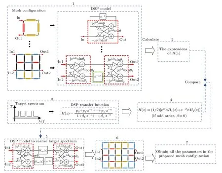
Fig.4. A flow chart of the DSP-based design process.
4. Design examples of integrated waveguide mesh
As an example, a 5-order square-wave interleaver with a duty cycle of 1:2(symmetrical interleaver), a free spectral range(FSR)of 100 GHz,and isolation<−30 dB is designed.
The transfer function of a digital elliptic low-pass filter that satisfies the required spectral characteristics can be expressed as

By using the pole interlacing properties,the transfer function can be decomposed as

After comparing Eq.(15)with Eqs.(2)and(3),it can be seen that an MZI with a double ring resonator structure on both arms with the arm length difference ofN×BUL can be used to realize the target spectral characteristics. The ratio of two polynomials in Eq. (15) is the transfer function of the double-ring resonator in the upper and lower arms, respectively. By comparing the expression with Eq.(4)and making them equal,the structural parameters of the double-ring resonator can be obtained. The DSP model,optical layout,and detailed structural parameters of the corresponding square-mesh configuration are shown in Fig.5(a)and Table 1,respectively. The obtained transmission spectra at the two output ports are presented as the green lines in Fig.5(c).We can see that the double-ring resonator becomes a single-ring resonator with doubled ring length to satisfy the requirements.

Fig.5. The DSP models and corresponding layout of square-mesh configurations for(a)5-order and(b)4-order square-wave interleavers with a duty cycle of 1:2. (c)Corresponding transmission spectra of the two output ports.
Similarly, an even-order square-wave interleaver can be designed. For the same target spectral requirements, if the filter order is 4,its transfer function can be obtained as

Then,Eq.(16)can be decomposed into the sum of two all-pass functions

It can be seen that an MZI with two cascaded single-stage ring resonators on each arm with appropriate phase delays can be configured to realize the target spectral characteristics. The four ratios of two polynomials in Eq.(15)are the transfer functions of the single-stage ring resonator in the upper and lower arms,respectively. By comparing the expression of the ratio with Eq.(2)to make them equal, the structural parameters of the ring resonator can be obtained. The DSP model and optical layout of the square mesh are shown in Fig.5(b). Table 1 gives its detailed structural parameters. The obtained transmission spectra at the two output ports are presented as the red lines in Fig.5(c).
According to this design method, square-wave interleavers with other duty cycles (asymmetrical interleavers) can also be obtained. Figure 6(a)shows the layout of the square mesh configuration for an asymmetrical 5-order interleaver. The detailed structural parameters of the mesh are given in Table 2. The transmission spectra at one of the output ports are presented as the red,green,and blue lines in Fig.6(b),respectively.
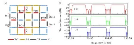
Fig.6. (a)The layout of the square mesh configuration for an asymmetrical 5-order interleaver. (b)Corresponding transmission spectra of the interleaver with duty cycles of 1:3,1:4,and 1:5.
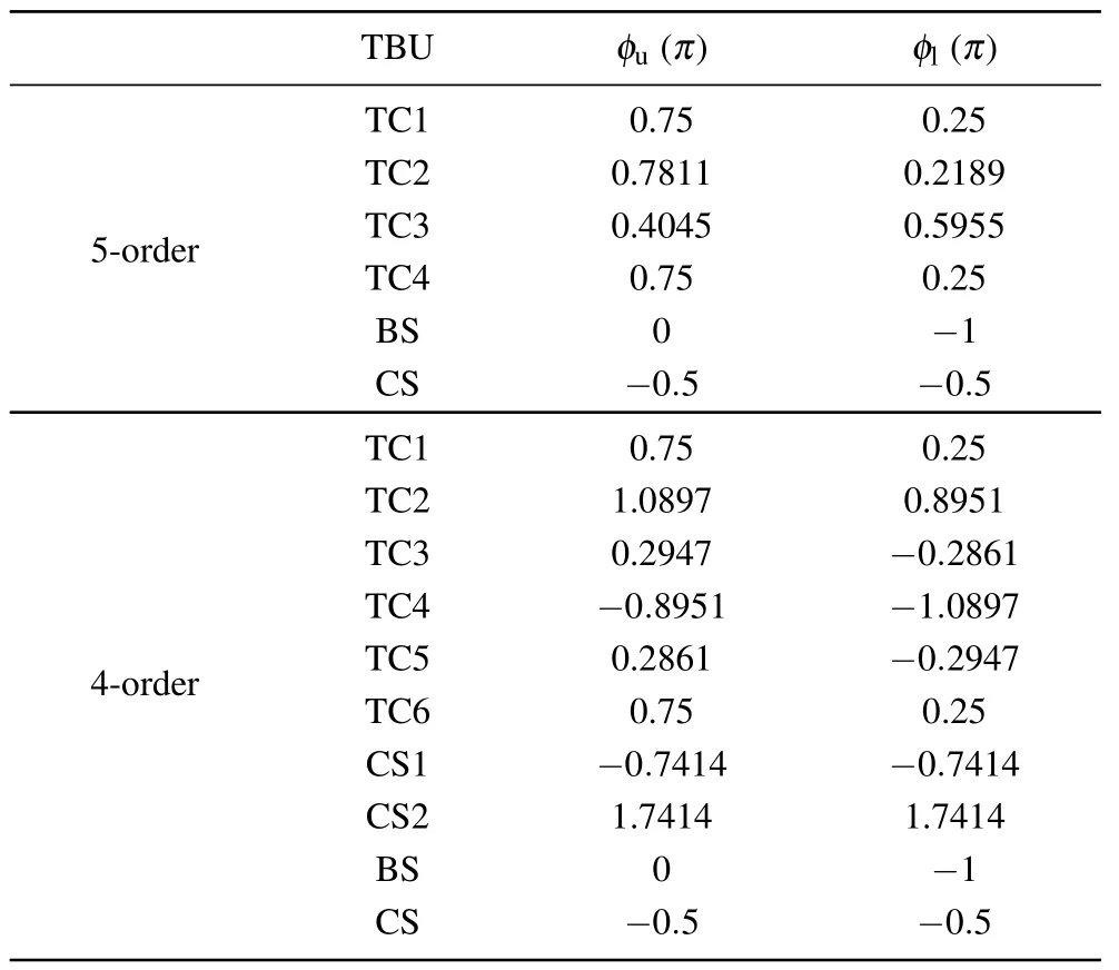
Table 1. Structural parameters of TBUs in the square mesh for 5-order and 4-order square-wave interleavers with a duty cycle of 1:2.

Table 2. Structural parameters of TBUs in the square mesh for a 5-order square-wave interleaver with duty cycles of 1:3,1:4,and 1:5.
The square mesh configurations for asymmetrical 4-order interleavers are the same as that of the symmetrical one but with different structural parameters,as shown in Table 3.
It can be seen from the above results that the higher the filter order,the closer the transmission spectra of the filter is to the ideal square wave(with a higher rectangular degree). Both even- and odd-order interleavers can be designed to achieve arbitrary duty cycles with different mesh configurations. For the same odd order, the mesh configurations of symmetrical interleavers are different from those of asymmetrical ones.While, for the same even order, the mesh configurations are the same for symmetrical and asymmetrical interleavers. Additional phase delay is needed on both arms for the even-order interleavers, whereas it is not necessary for odd-order ones.The even-order interleavers have a cascaded structure of multiple single-stage ring resonators on both arms, whereas the odd-order ones are not cascaded structures.

Table 3. Structural parameters of TBUs in the square mesh for 4-order square-wave interleavers with duty cycles of 1:3,1:4,and 1:5.
5. Discussion
5.1. Comparison of different mesh configurations
Different mesh geometries have different figures of merit.[18]Here, triangular, hexagonal, and square mesh are compared in terms of the square-wave properties. The FSR of a square-wave interleaver can be expressed as[18]

whereCis the speed of light in vacuum, andL=N×BUL is the total length of TBUs in the ORR. Due to different values ofNfor different mesh configurations, the BUL for the same FSR is different for triangular, square, and hexagonal mesh configurations. For an FSR = 100 GHz, the BUL is about 240µm,180µm,and 120µm for the triangular,square,and hexagonal mesh configurations, respectively, if the typical silicon-on-insulator(SOI)withng=4.18 is used. Table 4 lists the possible values of the FSR for triangular,square,and hexagonal mesh configurations with a BUL of 240 µm. The corresponding total ring lengthLis also shown. It can be seen from the table that the FSR can be 100 GHz, 50 GHz,33.3 GHz,25 GHz,20 GHz,16.7 GHz,...,100/nGHz withL=3n×BUL (n=1,2,3,...) for the triangular mesh configuration, 75 GHz, 37.5 GHz, 25 GHz, 18.8 GHz, 15 GHz,..., 75/nGHz withL= 4n×BUL (n= 1,2,3,...) for the square mesh configuration, and 50 GHz, 30 GHz, 25 GHz,21.4 GHz,18.8 GHz,16.7 GHz,15 GHz,...,150/(4+n)GHz withL=6×BUL, (8+2n)×BUL (n=1,2,3,...) for the hexagonal mesh configuration,respectively.Specific values of the FSR can be obtained with a selected mesh configuration,and the maximum number of FSRs(7 different FSRs)can be obtained with the hexagonal mesh configuration for the same range of total length from 1×BUL to 20×BUL.
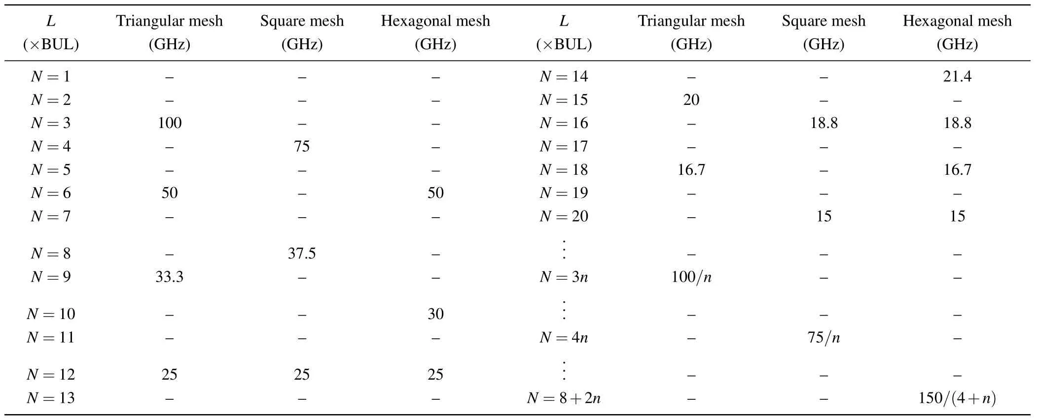
Table 4. Possible values of FSR for different mesh configurations with a BUL=240µm. The corresponding total ring length L is also shown.
The square mesh configuration for a 4-order square-wave interleaver with a duty cycle of 1:2 is shown in Fig. 5(b).A total of 31 TBUs have been used and the total size is 16×BUL2. Figure 7 shows the layout of hexagonal and triangular mesh configurations with the same filter orders and duty cycles. The configurations are the standard square-wave interleaver configuration.[31]For a hexagonal mesh configuration,39 TBUs are needed,and the total size is. For a triangular mesh configuration,27 TBUs are needed,and the total size is.

Fig. 7. The layout of (a) hexagonal and (b) triangular mesh configurations for a 4-order square-wave interleaver with a duty cycle of 1:2.
5.2. Influence of design and fabrication errors
In practical applications, there are various possible sources of errors, both in design and fabrication, that cause imperfect behavior of the TBUs, which will then introduce parasitic behavior in the mesh. These errors (which mainly include phase errors, and insertion loss) can accumulate and deteriorate the transmission spectrum of the circuit.[32]Taking the square mesh configuration (shown in Fig. 5(b)) as an example,the influence of the errors on the transmission characteristics of the circuit is discussed.All the TBUs are numbered as shown in Fig.8(a).
Firstly,the influence of the phase error of a single TBU in different states is discussed.
TBUs in the cross stateThe influence of the variation ofφu(orφl)for TBUs 1–4 on the transmission spectra is similar.The variations ofφuandφlhave almost the same influence on the transmission spectra for each TBU.A typical transmission spectrum is shown in Fig.8(b).It can be seen that the variation ofφu(orφl)for TBUs 1–4 only increases the insertion loss of the system,while the ripple of the passband and stopband,and the isolation are not changed. The positive and negative variations ofφu(orφl)have the same influence on the transmission spectra. A larger variation ofφu(orφl)would result in a larger 3-dB bandwidth.
A typical result of the influence of the variation ofφufor TBU 5 on the transmission spectra is shown in Fig.8(c). The influence of the variation ofφufor TBUs 6–12 on the transmission spectra is similar to that for TBU 5(not shown here).The variations ofφuandφlhave almost the same influence on the transmission spectra for TBUs 5–12 as well. It can be seen that the variation ofφu(orφl) for TBUs 5–12 increases insertion loss,the ripple of the passband and stopband,and the isolation. The 3-dB bandwidth also increases with the variation ofφu(orφl), which is a little larger than that for TBUs 1–4. Besides,the positive and negative variations ofφu(orφl)on the transmission spectra are different.

Fig.8. (a)The mesh configuration of the designed interleaver;(b)transmission spectra with different variations of φu for TBU 1;(c)transmission spectra with different variations of φu for TBU 5; (d) transmission spectra with different variations of φu for TBU 13; (e) transmission spectra with different variations of φu for TBU 25;(f)transmission spectra with different variations of φu for TBU 26;(g)transmission spectra with different variations of φu for TBU 28;(h)transmission spectra with different variations of φl for TBU 28. The insets show enlarged passbands.
TBUs in the bar stateA typical result of the influence of the variation ofφufor TBU 13 on the transmission spectra is shown in Fig.8(d). Similar results can be obtained for TBUs 14–24(not shown here).The variation ofφufor TBU 25 on the transmission spectra is shown in Fig.8(e).The variations ofφuandφlalso have almost the same influence on the transmission spectra for TBUs 13–25.We can see that the variation ofφu(orφl)for TBUs 13–24 and 25 increases the insertion loss,the ripple of the passband and stopband,and the isolation. For TBUs 13–24,the ripple of the passband and stopband is asymmetrical,and the positive and negative variations ofφu(orφl)have different influences on the transmission spectra. Whereas,for TBU 25, the passband and stopband have equal ripples, and the positive and negative variations ofφu(orφl)have the same influence on the transmission spectra.
TBUs in the tunable coupler stateA typical result of the influence of the variation ofφufor TBU 26 on the transmission spectra is shown in Fig. 8(f). The influences of the variations ofφufor TBUs 26 and 27 are similar,and the variations ofφuandφlhave almost the same influence on the transmission spectra for the two TBUs. The variation ofφu(orφl)for TBUs 26 and 27 only increases the insertion loss,isolation,and bandwidth. The positive and negative variations ofφu(orφl) have the same influence on the transmission spectra. The influence of the variation ofφuandφlfor TBU 28 on the transmission spectra is shown in Figs. 8(g) and 8(h), respectively.Similar results can be obtained for TBUs 29–31 (not shown here). It can be seen thatφuandφlhave different influences on the transmission spectra. The variation ofφuandφlfor TBUs 28–31 mainly increases the ripple of the passband and stopband,the isolation,and bandwidth.The ripple of the passband and stopband is asymmetrical as well,which is similar to TBUs 13–24.
By comparing Figs. 8(b)–8(h), we can see that for the small variation(±0.02π),the phase shift of TBUs 1–4 has little effect on device characteristics,whereas that of TBUs 28–31 and 13–24,which form resonators,has a greater influence.

Fig.9. Transmission spectra at the output port 1(or 2)with an insertion loss of 0.2 dB and(a)variation of φu,(b)variation of φl,and(c)simultaneous variations of φu and φl for all TBUs. (d)Transmission spectra at all ports with an insertion loss of 0.2 dB and δφu of 0.02π. The insets show enlarged passbands.
For a PPIC,when multiple TBUs have phase errors,there is a higher possibility that light will leak into adjacent paths and cause undesired interference(crosstalk)within the circuit.Furthermore, when additional insertion loss is introduced in multiple TBUs, the light intensity will be attenuated. Figure 9(a) shows the transmission spectra at output port 1 (or2)with an insertion loss of 0.2 dB andδφuof 0,±0.02π,0.1πfor all TBUs,respectively.For comparison,the ideal transmission spectrum without phase errors and insertion loss is also shown. It can be seen that the flat-top transmission decreased obviously when a 0.2dB insertion loss was considered. When the variation ofφuis small, the positive and negative variations ofφuhave almost no significant different influence on the spectrum. However,the transmission spectrum changes obviously (especially for the isolation), and the center frequency shifts greatly when the variation ofφuis large. For the positive/negative variation ofφu,the transmission spectrum shifts to a high-frequency/low-frequency direction. The influence of the variation ofφl,and simultaneous variations ofφuandφlare shown in Figs.9(b)and 9(c),respectively. The shift direction of transmission spectra is opposite for the variations ofφuandφl. Besides the prescribed output ports (1 and 2), due to the leakage of light in all adjacent TBUs,the light will also output from all other ports of the circuit. Figure 9(d)shows the result of this whenδφuequals 0.02πfor all TBUs. The upper two curves in the figure are the transmission of output ports 1 and 2, and the remaining ones are those of other ports. We can see that although most signals are transmitted to output ports 1 and 2 with high transmission, a small part of the signals is leaked out through other ports simultaneously.
6. Conclusion
In this paper, from the perspective of DSP, the digital signal model of the PPIC is established. Based on this, a software-defined general design method for the PPIC is established using mature DSP technology and algorithm. The DSP design method establishes the relationship between optical and electrical signals, which is especially suitable for the design of the optoelectronic hybrid system, and which is not a feature of the conventional optical design method. To show the feasibility of this technique, photonic waveguide meshes with square configurations are designed to realize optical signal interleaving with tunable duty cycles. The influence of the shape of the mesh cell (mesh configuration) and the design and fabrication errors(which mainly include phase errors and insertion loss)of the tunable basic unit(TBU)on the performance of the interleavers is discussed in detail. The DSP approach offers an effective pathway for the establishment of a general design platform for software-defined PPICs.
猜你喜欢
杂志排行

Chinese Physics B的其它文章
- High sensitivity plasmonic temperature sensor based on a side-polished photonic crystal fiber
- Non-Rayleigh photon statistics of superbunching pseudothermal light
- Refractive index sensing of double Fano resonance excited by nano-cube array coupled with multilayer all-dielectric film
- A novel polarization converter based on the band-stop frequency selective surface
- Effects of pulse energy ratios on plasma characteristics of dual-pulse fiber-optic laser-induced breakdown spectroscopy
- Simulation of detection and scattering of sound waves by the lateral line of a fish