Refractive index sensing of double Fano resonance excited by nano-cube array coupled with multilayer all-dielectric film
2022-02-24XiangxianWang王向贤JianZhang张健JiankaiZhu朱剑凯ZaoYi易早andJianliYu余建立
Xiangxian Wang(王向贤) Jian Zhang(张健) Jiankai Zhu(朱剑凯) Zao Yi(易早) and Jianli Yu(余建立)
1School of Science,Lanzhou University of Technology,Lanzhou 730050,China2Joint Laboratory for Extreme Conditions Matter Properties,Southwest University of Science and Technology,Mianyang 621010,China3School of Electronic Engineering,Chaohu University,Chaohu 238000,China
We propose a hybrid structure of a nano-cube array coupled with multilayer full-dielectric thin films for refractive index sensing. In this structure,discrete states generated by two-dimensional grating and continuous states generated by a photonic crystal were coupled at a specific wavelength to form two Fano resonances. The transmission spectra and electric field distributions of the structure were obtained via the finite-difference time-domain method. We obtained the optimal structural parameters after optimizing the geometrical parameters.Under the optimal parameters,the figure of merit(FOM)values of the two Fano resonances reached 1.7×10⁴ and 3.9×10³,respectively. These results indicate that the proposed structure can achieve high FOM refractive index sensing,thus offering extensive application prospects in the biological and chemical fields.
Keywords: Fano resonance,refractive index,nano-cube array,all-dielectric film
1. Introduction
Owing to rapid development in fabrication technology,complex micro-nano structures have become a reality in recent years. When the size of a material enters the micro-nano scale,it creates multiple new effects in micro-nano structures,such as those of the surface local field, quantum size, and macroscopic quantum tunneling. These effects cause micronano materials to exhibit specific mechanical,thermal,optical,electrical, and magnetic properties. Studying the novel properties of micro-nano materials is vital for optical physics research;it promotes the development of micro-nano materials.Micro-nano structures are widely used in photocatalysis,[1,2]photonic crystals,[3,4]surface-enhanced Raman scattering,[5,6]and solar absorption.[7–10]In addition,optical refractive index sensors[11–16]based on micro-nano structures have garnered significant interest as they can dynamically detect the refractive index of a sample by identifying the formant drift in the spectral curve.
Spectral curves predominantly have a symmetric Lorentz line and an asymmetric Fano line.[17–19]However, when the sensing characteristics of the sensing structure are described using Lorentz lines, the optical characteristics are relatively simple, limiting the diversity of the sensing structures.[20]In contrast to the formation mode of Lorentz resonance,Fano resonance is caused by destructive interference between the discrete states and adjacent states. It has a very high slope spectrum and strong dispersion.[21,22]Strongly constrained electric fields can enhance the interaction between light and matter significantly. In addition, Fano resonance is very sensitive to geometric parameters and medium environment. Moreover,a multiple Fano resonance structure is advantageous when compared to a single Fano resonance structure as the former provides more reliable results than the latter and can even be implemented with multispectral sensors.[23]Therefore, its parallel processing capability offers tremendous advantages in chip-level optical circuits that can be applied in sensors and other fields.[24–28]
This study proposed a hybrid structure coupled with multilayer full-dielectric thin films and a nano-cube array that can excite two independently tunable Fano resonances. We explain the cause of Fano resonance by using analogue simulation. In other words, upon satisfying the phase-matching condition,a guided-mode resonance that provides two narrowband discrete states was generated in the two-dimensional array grating structure. A photon gap was formed in the Fabry–Pérot-like(F–P-like)cavity containing periodic photonic crystals in order to establish a continuous state. Fano resonance is produced by destructive interference between the continuous state and the discrete state at a specific wavelength. In addition, the influence of geometrical variables on resonance behavior was discussed in detail,and suitable geometrical parameters for RI sensing were obtained. Finally, an important physical parameter, FOM, was used to describe the sensing performance of the structure.
2. Structure model and analytical method
Figure 1(a)presents a schematic diagram of the designed hybrid structure. The upper half is a cubic nano-array struc-ture, primarily comprising a two-dimensional grating layer and a waveguide layer. For the convenience of fabrication,SiO2dielectric material was used for the two-dimensional grating layer and waveguide layer. Figure 1(b) illustrates a top view of the structure in theX–Ysection.landware the length and width of the nano-cube,respectively;PxandPyrepresent the periods in thexandydirections, respectively. The lower half was the F–P-like cavity containing photonic crystals, composed of four layers of Si and TiO2. To ensure the optimal sensing performance of the structure,the thickness of the Si and TiO2layers was maintained at 36 nm and 65 nm,respectively. The bottom layer of the structure was manufactured using SiO2. The coupling layer consisted of MgF2and had a thickness ofdc=125 nm;it was located below the waveguide layer and adjacent to the Si layer. The refractive index of the selected MgF2is 1.37, which is lower than that of SiO2in the waveguide layer of 1.45. The refractive index of the analyte is also lower than that of the waveguide layer.Therefore, diffraction waves are generated in the waveguide layer when incident light passes through the cube array,resulting in total reflection. The thickness of MgF2simultaneously affects the transmission mode of incident light and the position of the formant,due to which MgF2is selected for the coupling layer.

Fig. 1. Schematic diagram of the sensing structure. (a) Three-dimensional structure. (b)Top view of the structure in the X–Y section. Px and Py are the periods in two directions, whereas w and l are the width and length of the nano-cube,respectively.
The preparation process of the micro-nano structure is as follows. The quartz substrate is first ultrasonically cleaned using acetone,isopropanol,and deionized water. Subsequently,four layers of 36 nm Si film and 65 nm TiO2film are deposited on the quartz substrate using the electron beam evaporation method. A 125 nm MgF2film and a 90 nm SiO2film are then deposited on the Si film through electron beam evaporation.Following this, a layer of photoresists is spin-coated on the SiO2film using pre-baking, exposure, development, hardening and other steps. A cubic aperture array with a length of 330 nm and a width of 280 nm is formed on the photoresist layer, and a layer of 100 nm SiO2film is deposited via electron beam evaporation. Lastly, the lift-off process is used to obtain the complete structure.
Fano resonance requires a dark mode that provides a discrete state and a light mode that provides a continuous state.First,the formation of discrete states is discussed.The diffraction condition of the grating can be expressed as[29]

wherePrepresents the period of the SiO2cubes,nrepresents the refractive index of the waveguide layer,θmrepresents the diffraction angle,θiis the incident angle,andλ0represents the wavelength in the vacuum. A part of the light incident on the surface of the grating is transmitted directly due to the diffraction effect of the grating, and moiety light is propagated in the waveguide layer. Some of the light trapped in the waveguide layer is diffracted outwards and destructively interferes with the transmitted part of the beam,creating a guided-mode resonance.[29–32]The guided mode resonance condition can be expressed as

whereφ1andφ2represent the phase differences caused by the total reflection between the waveguide layer and the coupling layer interface and sensing interface, respectively. This ensures that most of the light is confined to the waveguide layer.Figure 3 illustrates the electric field distribution of the guided mode resonance,and it can be observed that the energy of the electric field is concentrated in the waveguide and coupling layers. Consequently, the energy of the transmitted light reduces drastically, forming a narrow-band discrete state in the transmission spectrum that provided a discrete state for the formation of Fano resonance,as shown in Fig.2(a).

Fig.2. Transmission spectrum of structures. (a)Discrete state spectral lines of two-dimensional gratings. (b)Continuous state spectral lines of the F–Plike cavity.
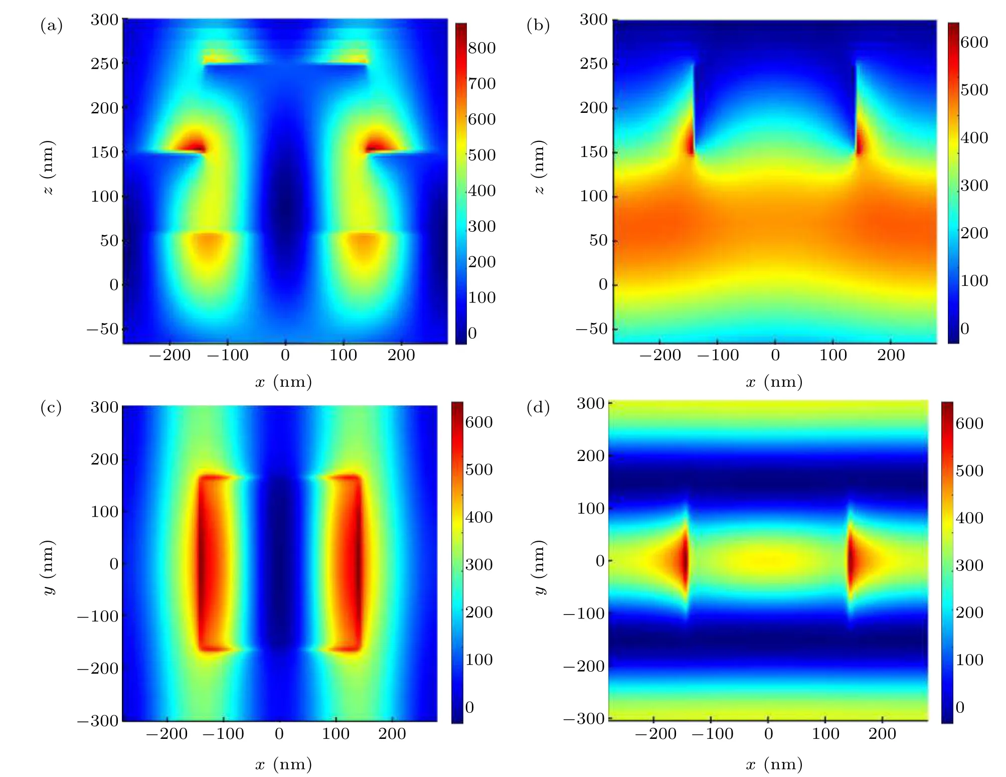
Fig. 3. The electrical field intensity profile at the X–Z plane for the guided mode resonance at (a) 646 nm and (b) 731 nm. The electrical field intensity profile at X–Y plane for the guided mode resonance at(c)646 nm and(d)731 nm.

Fig.4. The spectral curve of Fano resonance.
Next, the formation of a continuous state is discussed.When the incident light propagated in the waveguide layer,part of the light passed through the waveguide layer and entered the F–P-like cavity. According to the structural characteristics of the F–P-like cavity, total reflection will occur in the cavity. However, photon localization will occur when the light wave propagates to the periodic photonic crystal,forming a photon gap.[33]Therefore, a wider frequency band was obtained,providing a continuous state for the formation of Fano resonance,as demonstrated in Fig.2(b).
Consequently, the Fano resonance in the transmission spectrum of the entire structure was formed due to the interference of the narrow-band discrete state and wide-band continuous state. Figure 4 illustrates the transmission spectrum,denoted by the solid black line. Evidently, two Fano resonances with asymmetrical ultra-sharp line shapes occurred in this structure,represented as Fano 1 and Fano 2,respectively.
We also calculated the electric field distribution at resonance wavelengths under the two Fano resonances. Figures 5(a)and 5(b)respectively show the electric field distributions of Fano 1 and Fano 2 in theX–Zplane along the grating center.Most of the energy was concentrated at the top and surrounding area of the grating. Figures 5(c)and 5(d),depicting the electric field distribution in theY–Zplane,indicate that almost all the energy was concentrated in the waveguide layer and grating. In addition,according to Figs.5(e)and 5(f),there was a large amount of electric field energy on the surface of the waveguide layer. Therefore, the surface electric field in the sensing area could be enhanced to determine the sensing characteristics of the sample to be tested.
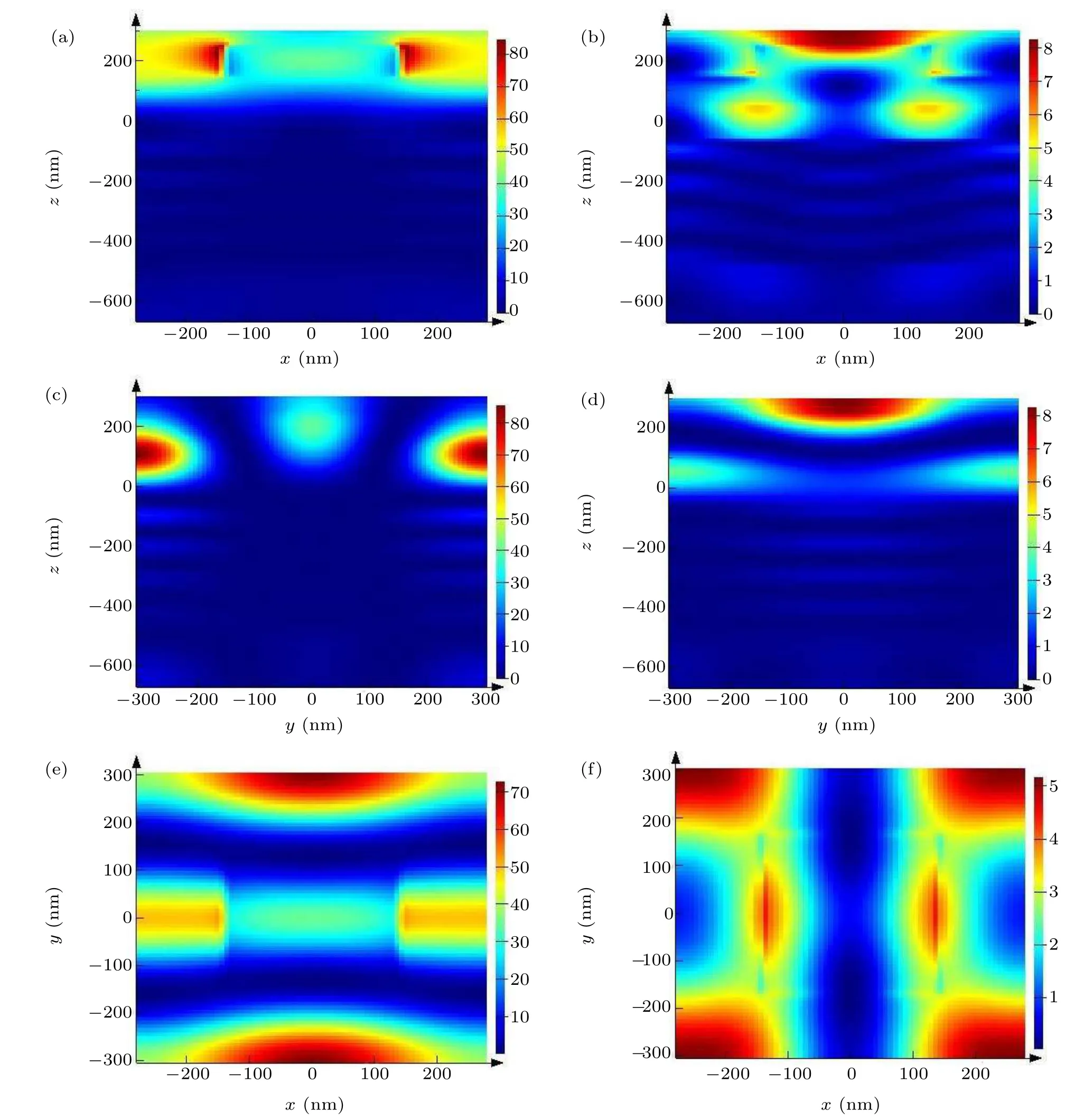
Fig.5. Electric field distribution at the resonance wavelengths of(a),(c),(e)654 nm(Fano 1)and(b),(d),(f)671 nm(Fano 2).
3. Structural optimization
We further explored the influences of geometric parameters on transmission characteristics and used refractive index sensing to determine optimal sensing characteristics for the proposed structure. According to Eqs.(1)and(2),guided mode resonance is related to grating period, waveguide refractive index and waveguide thickness. Different diffraction waves are generated when the light wave is incident on the cubic nano-array with different periods,thus affecting the generation of Fano resonance.Figure 6(a)demonstrates the changes in the spectral lines in the discrete state asPxincreased from 540 nm to 580 nm in increments of 10 nm. The first peak of the discrete state shows a redshift with the increase ofPx,while the second peak is unchanged,indicating thatPxprimarily affected the first peak. Simultaneously,the spectral line Fano 2 in the coupling state had a noticeable redshift and a downward trend in its transmittance with the increase inPx, as depicted in Fig.6(b). Remarkably,the spectral lines of Fano 1 did not change with thePxperiod. In addition, the coupling of the continuous state and first peak of the discrete state induced the formation of Fano 2, which was primarily affected by thePxperiod.This also explains the reason for the formation of Fano 2 from another aspect. ThePxperiod was selected at 560 nm as it provided the most favorable peak transmission for the two Fano resonances.

Fig. 6. Influences of 2D grating period Px on (a) discrete spectral line, (b)Fano resonance spectral line.
Figure 7(a) shows the variations in the spectral lines in the discrete state whenPyincreased from 590 nm to 630 nm in increments of 10 nm. The second peak of the discrete state showed a redshift phenomenon with the increase inPy.In contrast,as reflected in the spectral line of Fano resonance,Fano 1 showed a redshift with the increase inPy,and the transmission first increased and then decreased. However,Fano 2 remained almost unchanged. This indicates that the coupling of the continuous state and second peak of the discrete state caused the resonance of Fano 1, withPyperiod being the primary influencing factor. In addition, the spectral lines indicate that the sensing performance was best whenPy=610 nm.
The coupling layer forms the mutual layer of the twodimensional grating and F–P-like cavity. The thickness of MgF2affects the transmission mode of the incident light and the position of the formant. Figure 8 illustrates the influence of the coupling layer thicknessdcon the Fano spectral curves whendcincreased from 115 nm to 135 nm in increments of 5 nm. As seen from the figure,the coupling layer was essential for the Fano effect.Although both Fano peaks showed redshift,the redshift of Fano 1 was more pronounced when compared to Fano 2.In addition,asdcincreased,the transmittance for Fano 1 decreased, whereas that for Fano 2 first increased and then decreased.Upon noting these observations,the thickness of the coupling layer was selected asdc=125 nm to obtain better sensing performance.

Fig. 7. Influences of 2D grating period Py on (a) discrete spectral line, (b)Fano resonance spectral line.

Fig.8. Influence of coupling layer thickness dc on transmission spectrum.
We also explored the influence of the dimensions of cube nanoparticles on the transmittance spectra. Figures 9(a)–9(c)display the variation in transmission spectrum with the increase in grating width(w),length(l),and height(h),respectively.
Initially,both Fano 1 and Fano 2 reported a slight redshift whenwincreased from 260 nm to 300 nm in increments of 10 nm. The transmittance intensity of Fano 1 remained unchanged;however,Fano 2 exhibited a pronounced variation in the transmittance. The Fano 1 and Fano 2 transmittance was lowest atw=270 nm and highest atw=280 nm. Therefore,optimal grating width was selected as 280 nm. Thereafter,the length of the grating changed. According to Fig.9(b),the two Fano peaks showed no displacement changes with an increase in grating length. The only noteworthy observation was the peak transmittance of Fano 2 atl=330 nm;therefore,the optimal grating length was selected as 330 nm.

Fig. 9. Effect of grating geometry parameter on Fano resonance spectral curve. (a)Effect of grating width on Fano resonance spectral curve. (b)Effect of grating length on Fano resonance spectral curve. (c)Effect of grating height on Fano resonance spectral curve.
The grating height was increased fromh= 80 nm toh=120 nm in increments of 10 nm. According to Fig. 9(c),both Fano peaks showed a redshift phenomenon. The transmittance of Fano 1 and Fano 2 increased first and then decreased, but the change of Fano 2 was more prominent than that of Fano 1. In addition,Fano 2 had the best transmittance whenh=100 nm. Consequently, the optimal grating height was selected as 100 nm.
4. Sensing performance of the structure
The abovementioned observations indicate that changing the geometric parameters of the structure can effectively tune the resonance wavelength and spectrum line shape of the Fano resonance.Accordingly,the optimum geometric parameters of the hybrid structure to be used for refractive index(RI)sensing werePx=560 nm,Py=610 nm,dc=125 nm,w=280 nm,l=330 nm,andh=100 nm.
These structural parameters could determine the sensing performance of the hybrid structure. Sensitivity (S) and figure of merit(FOM).[34,35]are essential parameters for sensors.They are calculated as follows:S=Δλ/Δn, where Δnrepresents the refractive index variation in the surrounding environment and Δλis the wavelength shift caused by the refractive index change;FOM=ΔT/(ΔnT),whereTis the transmission of the structure and ΔT/Δndenotes the transmission change at a fixed wavelength induced by a refractive index change.Figure 10(a)shows the changes in resonance wavelength corresponding to the analyte RI from 1.00 to 1.10 in incremental steps of 0.02. According to the figure, a slight increase in the refractive index led to a significant redshift in the entire spectrum. The above properties are described in detail in Fig. 10(b), which demonstrates the relationship between the resonance wavelength and analyte RI. Using the abovementioned formula,the sensitivity of Fano 1 and Fano 2 were calculated as 234.7 nm/RIU and 111.4 nm/RIU,respectively.Figure 10(c)presents the FOM curve.There is a maximum at each dip of the transmission spectrum. At refractive index 1.01,the values of FOM at 654 nm and 671 nm were 1.7×10⁴and 3.9×10³, respectively. The structure designed in this study can generate two mutually independent tunable Fano peaks,which can be used as a self-reference in sensing applications,unlike the subwavelength dielectric grating coupled photonic crystal structure proposed in reference[20]that can generate an ultra-high FOM value. Moreover, the proposed sensor structure is advantageous in terms of the maximum FOM value when compared to the sensing structures reported in previous studies.[24–28]Therefore, the proposed system is suitable for sensor applications. The resonance quality factorQ-factor is also a key parameter that affects the sensing performance. TheQ-factor of the resonances can be defined as the ratio between the wavelength of each resonance peak,λ,and the full-width at half-maximum(FWHM),i.e.Q=λ/FWHM. For the Fano resonances with asymmetric line shapes, the FWHM can be considered as the full width between the peak and the trough of each Fano resonance peak.[36]This study discusses the quality factors of two Fano resonances separately, as shown inFig.10(d). TheQ-factor of Fano 1 increases with the increase in the refractive index, and the maximumQ-factor can reach the value of 10592. TheQ-factor of Fano 2 also increases,but not as drastically as that of Fano 1. The maximumQ-factor of Fano 2 is 5374. TheQ-factor of the proposed structure is significantly improved when compared to those of previous studies.[36–39]Therefore,the proposed structure has good sensing performance and can be used as a gas sensor.

Fig.10. (a)Transmission spectrum of the structure when the analyte RI varies from 1.0 to 1.1 in incremental intervals of 0.02. (b)The relationship between the resonance wavelength of Fano 1 and Fano 2 with analyte n. (c)FOM of Fano 1 and Fano 2. (d)Q-factor of Fano 1 and Fano 2.
5. Conclusion
We proposed a micro-nano-structure coupled with multilayer full-dielectric thin films and a nano-cube array that can excite two independently tunable Fano resonances to study gas sensors. Fano 1 and Fano 2 formant peaks were generated by coupling the discrete and continuous states at a particular wavelength. The effects of the structure parameters on the two Fano resonance spectra were analyzed by using numerical simulation,and the optimal structure parameters were obtained. The refractive index of the sample was dynamically detected at optimal structure parametersPx=560 nm,Py=610 nm,dc=125 nm,w=280 nm,l=330 nm, andh=100 nm. The FOM values of Fano 1 and Fano 2 were 1.7×10⁴and 3.9×10³,respectively. These results show that the proposed structure can achieve refractive index sensing with high FOM and has broad application prospects in biology and chemistry.
Acknowledgments
Project supported by the National Natural Science Foundation of China(Grant No.61865008)and the Hong Liu First-Class Disciplines Development Program of Lanzhou University of Technology.
猜你喜欢
杂志排行

Chinese Physics B的其它文章
- High sensitivity plasmonic temperature sensor based on a side-polished photonic crystal fiber
- Digital synthesis of programmable photonic integrated circuits
- Non-Rayleigh photon statistics of superbunching pseudothermal light
- A novel polarization converter based on the band-stop frequency selective surface
- Effects of pulse energy ratios on plasma characteristics of dual-pulse fiber-optic laser-induced breakdown spectroscopy
- Simulation of detection and scattering of sound waves by the lateral line of a fish