A density-wave-like transition in the polycrystalline V3Sb2 sample with bilayer kagome lattice
2022-01-23NingningWang王宁宁YuhaoGu顾雨豪McGuireJiaqiangYanLifenShi石利粉QiCui崔琦KeyuChen陈科宇YuxinWang王郁欣HuaZhang张华HuaixinYang杨槐馨XiaoliDong董晓莉KunJiang蒋坤JiangpingHu胡江平BosenWang王铂森JianpingSun孙建平andJinguangCheng程金光
Ningning Wang(王宁宁) Yuhao Gu(顾雨豪) M.A.McGuire Jiaqiang Yan Lifen Shi(石利粉)Qi Cui(崔琦) Keyu Chen(陈科宇) Yuxin Wang(王郁欣) Hua Zhang(张华) Huaixin Yang(杨槐馨)Xiaoli Dong(董晓莉) Kun Jiang(蒋坤) Jiangping Hu(胡江平) Bosen Wang(王铂森)Jianping Sun(孙建平) and Jinguang Cheng(程金光)
1Beijing National Laboratory for Condensed Matter Physics and Institute of Physics,Chinese Academy of Sciences,Beijing 100190,China
2School of Physical Sciences,University of Chinese Academy of Sciences,Beijing 100190,China
3Materials Science and Technology Division,Oak Ridge National Laboratory,Oak Ridge,Tennessee 37831,USA
Keywords: V3Sb2,kagome metal,charge density wave,pressure effect
1. Introduction
The kagome lattice compounds consisting of cornershared triangular network have been the focus of extensive investigations over last decades because they can host fascinating physical phenomena ranging from geometrically frustrated magnetism to nontrivial band topology.[1-13]When the localized moments are situated on the kagome lattice, frustrated spin interactions can lead to exotic magnetic ground states such as the quantum spin liquid state extensively studied in the herbertsmithite ZnCu3(OH)6Cl2.[14-19]On the other hand, when the itinerant electrons are present, the metallic kagome lattice compounds hold the gene to achieve nontrivial electronic band structure containing Dirac cones,flat band,and van Hove singularities.[20-24]Upon proper electron filling, these features can promote novel correlated and/or topological states,such as bond density wave order,[23,25]valencebond state,[26]chiral spin-density-wave (SDW) order,[21]nontrivial charge-density-wave (CDW) order,[1,27-29]exotic superconductivity,[12,23,30]etc. Thus, much experimental effort has been devoted to the metallic 3d transition-metal-based kagome systems.
For the correlated magnetic kagome metals, the coexistence of spin and charge degrees of freedom leads to the emergence of many novel quantum phenomena with nontrivial electronic behaviors. For example, large anomalous Hall effect (AHE) and Dirac fermions have been realized in the ferromagnetic Fe3Sn2with flat-band dominated electronic band structure[7,31,32]and the quantum-limit Chern ferromagnet TbMn6Sn6.[13]Large intrinsic AHE has been observed in ferromagnetic Weyl semimetal Co3Sn2S2[6,33,34]and noncollinear antiferromagnetic Mn3Sn.[35]Dirac fermions have also been revealed in the antiferromagnetic FeSn.[10,36]For the recently discoveredAV3Sb5(A=K,Rb, Cs)family with quasi-2D ideal kagome layers of V ions,no static magnetic order was observed but they exhibit the coexistence and complex competition between superconductivity and chiral CDW in addition to giant AHE and pair density wave state.[12,27-29,37-54]For this latter class of materials, there are still many open issues, such as the nature of superconductivity and the mechanism of chiral CDW order.
Since the materials’ realizations are scarce, it is indispensable to find more metallic kagome lattice compounds. To this end,we focus our attention on a simple binary compound V3Sb2, which is isostructural to Fe3Sn2and contains bilayer kagome lattice of V ions.[31]This material has been known to exist at temperatures below 875±25°C in the V-Sb phase diagram,[55]but its physical properties have not been studied in detail to the best of our knowledge. In this work, we successfully synthesized nearly pure V3Sb2polycrystalline sample and then characterized its structure, electrical transport,magnetic, and thermodynamics properties at ambient or high pressures. Our results reveal a density-wave-like transition atTdw≈160 K, which is evidenced by a clear anomaly in both magnetic susceptibility and resistivity. This compound shows no long-range magnetic order and superconductivity down to 1.5 K even after the density-wave-like transition being suppressed completely by hydrostatic pressure.Since our densityfunctional-theory (DFT) calculations show that V3Sb2has a non-trivial topological crystalline property, the present study indicates that it may serve as a new metallic kagome system to study the interplay between density-wave-order, nontrivial band topology and possible superconductivity.
2. Experimental and calculation details
Polycrystalline samples of V3Sb2were synthesized by the traditional solid-state-reaction method. The powders of V (99.99%) and Sb (99.99%) in the molar ratio 3 : 2 were thoroughly mixed and pressed into a pellet, which was then placed into a quartz tube and sealed under high vacuum(~5×10⁻⁴Pa). The sealed ampoule was slowly heated to 700°C and held for 48 hours, and then sintered again at 750-850°C for 48 hours several times with intermediate grinding and pelletizing. According to the V-Sb phase diagram, the LT-phase of V3Sb2with the Fe3Sn2-type structure is stable below the peritectoid temperature of 875±25°C,above which the V-deficient V2-xSb phase is more stable.[55]Thus, we have kept the highest sintering temperatures below 850°C in order to obtain the LT-V3Sb2with the Fe3Sn2-type structure in the present study. Phase purity of the obtained V3Sb2polycrystalline samples was examined by powder x-ray diffraction (XRD) at room temperature with a CuKα1radiation. In order to extract the structural parameters, the refinements of the crystal structure were performed by the Rietveld method, using the FULLPROF program. Low-temperature XRD data in the temperature range 25-300 K were collected using an Oxford Phenix cryostat and a PANalytical X’Pert Pro MPD diffractometer(CuKα1radiation). The powder was mounted on an aluminum sample holder using Apiezon Ngrease. Highscore Plus was used for Rietveld analysis of the XRD patterns from V3Sb2.[56]
The magnetic properties were measured with a Quantum Design magnetic property measurement system (MPMS-III).Heat capacity and electrical transport measurements were carried out by using a Quantum Design physical property measurement system(PPMS,14 T).High-pressure resistivity was measured by using a self-clamped piston-cylinder cell under various hydrostatic pressures up to 1.81 GPa.[57]Daphne 7373 was used as the pressure transmitting medium and the pressure values were determined from the relative shift of the superconducting transition temperature of Pb.
Our DFT calculations employ the Viennaab initiosimulation package (VASP) code[58]with the projector augmented wave (PAW) method.[59]The Perdew-Burke-Ernzerhof (PBE)[60]exchange-correlation functional is used in our calculations. The kinetic energy cutoff is set to be 600 eV for expanding the wave functions into a plane-wave basis in VASP calculations while the energy convergence criterion is 10-6eV. TheΓ-centeredk-mesh is 8×8×8. The spin-orbital coupling is included in our DFT calculations.The calculation of topological indices employs vasp2trace program on Bilbao Crystallographic Server.[61-63]
3. Results and discussion
We have attempted to prepare pure V3Sb2samples by varying the final sintering temperatures between 750°C and 850°C. After tries and errors, we eventually obtained two V3Sb2polycrystalline samples with relatively high purity as examined by XRD. Hereafter, these two samples sintered at 780°C and 830°C are labeled as S1 and S2, respectively.Since their physical properties show some different behaviors,in the following we present the experimental results of both samples comparatively so as to underline the fact that the physical properties of V3Sb2are sensitive to the preparation conditions.
Figure 1 shows the XRD pattern of these two V3Sb2samples after Rietveld refinement. It confirms that the obtained samples are nearly single phase with a small amount of impurity, which can be identified as V3Sb for S1. The impurity phase is too weak to be identified for S2. The main phase of the XRD pattern can be refined by considering the hexagonal Fe3Sn2-type structure model(space groupR-3m,No.166)with one V position at the 18h (x,y,z) and two Sb positions at 6c (0, 0,z), respectively. As illustrated in Fig. 1, the refinements converge well with reliable factorsRp=2.66%,Rexp=2.48%,andχ2=2.28 for S1,andRp=2.98%,Rexp=2.26%, andχ2=3.78 for S2. According to the scaling factors, the amount of V3Sb impurity in S1 was estimated to be~1.2 wt%,which is consistent with the observed weak main peak of V3Sb as shown by asterisk in Fig.1(a). The obtained structural parameters for both samples are listed in Table 1 for comparison. As can be seen,the sample S1 has a shorterabut a longerc,leading to a slightly smallerVin comparison with those of sample S2. However,the differences are quite small,with the relative difference being smaller than 0.3%. These lattice parameters are also consistent with those reported in literature for LT-V3Sb2.[55]In contrary, the positions of the atoms,especially along thez-axis,show a relatively large difference. Taking the V site as an example,the difference of thez-axis position is about 2.5%for these two samples,which results in a difference in the bond length along thec-axis as discussed below. It should be noted that slight variation of V/Sb ratio in samples prepared at different conditions is possible and should be responsible for the observations of the sampledependent structural and physical properties shown below. In addition, synchrotron-based XRD is desirable to have more accurate determination of the structural details.

Fig.1. Observed(cross),calculated(solid line),and difference(bottom line) XRD profiles of the polycrystalline V3Sb2 samples: (a) S1 and(b) S2 after Rietveld refinements. Bragg positions of the main phase V3Sb2 and the impurity phase V3Sb are indicated by the two rows of tick marks in(a),while only the position of V3Sb2 is shown in(b). The main peak of the V3Sb impurity phase is marked by an asterisk in(a).The obtained lattice parameters for both samples are also given in the figure.
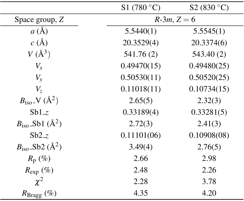
Table 1. Lattice parameters,atomic coordinates,and isotropic thermal factors Biso for V3Sb2 samples from powder XRD data at 295 K.
The crystal structure of V3Sb2is schematically shown in Fig. 2 by taking the refined structural information of S1. As seen in Fig. 2(a), the crystal structure of V3Sb2is composed of Sb1 single layer and V-Sb2 bilayer that are stacked alternatively along thec-axis. The Sb1 atoms in the single layer form a 2D graphene-like honeycomb lattice, Fig. 2(b), while the V-Sb2 bilayer consists of two V kagome layers with Sb2 atoms embedded in the center of the V hexagons, Fig. 2(c).For each V kagome layer, there are two kinds of equilateral triangles with different V-V bond lengths, i.e., 2.8600(19) ˚A and 2.6839(19) ˚A for S1[2.864(4) ˚A and 2.691(4) ˚A for S2],as shown in purple and blue in Fig. 2(d). This means that the kagome lattice is not ideal,different from that inAV3Sb5.As shown in Fig.2(e),the V atoms of the smaller V triangles in two adjacent layers can be viewed to form a V6octahedra with an interlayer V-V distance of 2.773(4) ˚A for S1 [2.870(6) ˚A for S2]. For S1, this value is equal to the average of two intralayer nearest-neighbor V-V bond lengths. Such a small interlayer distance should produce a relatively strong interlayer interaction. However, the interlayer V-V bond length for S2 is found to be~3% longer than the average in theabplane,which might result in weaker interlayer interactions.

Fig.2. (a)A schematic view of the layered structure of V3Sb2 (side view)stacked by Sb1 and V-Sb2 layers along the c-axis. The unit cell is enclosed by the dashed lines. (b) The Sb1 atoms form a honeycomb sublattice below and above each V-Sb2 bilayer with Sb1-Sb1 bond length of 3.20 ˚A. (c)The structure of the V-Sb2 layer. The V atoms form bilayer kagome lattice and the Sb2 atoms sit in the centers of the V hexagons in each V kagome layer. (d)Single V-Sb2 kagome layer made of two kinds of equilateral triangles with the side lengths of 2.8602 ˚A and 2.6839 ˚A,shown in purple and blue,respectively. (e)The V triangles with smaller length(blue)in two layers form the V6 octahedra. The bond-length values are taken from the refined results of the S1 sample.
Figures 3(a) and 3(b) show the temperature-dependent magnetic susceptibilityχ(T) of these two V3Sb2samples measured in the temperature range 1.8-300 K under an external magnetic field ofµH=1 T. The experimental procedure is following: we first cooled the sample under zero field from room temperature to the lowest temperature,then applied 1 T field and recordedχ(T) upon heating up to room temperature, followed by measuringχ(T) upon cooling down to the lowest temperature under 1 T. They are thus denoted as the ZFCw-and FCc-χ(T),respectively. As seen in Fig.3(a),the ZFCw-and FCc-χ(T)curves of S1 exhibit a step-like anomaly around 160 K,below which the magnetic susceptibility is reduced. In addition,an obvious thermal hysteresis is evidenced around the transition,implying a first-order nature of this transition. The transition temperatures,Tχdw, defined as the maximum of dχ/dT,are~159 K and~165 K for S1 in the cooling and heating processes, respectively, as shown in the top of Fig. 3(a). Theχ(T) curves of S2 are basically similar to those of S1, but the transition is much wide and the thermal hysteresis becomes very weak,Fig.3(b). In addition,the transition temperatures,Tχdw≈154 K and 158 K for the cooling and heating processes,are lower than those of S1. These comparisons indicate that the quality of S1 is better than that of S2. We note that the observed feature in the magnetic susceptibility is very similar to those seen in some typical CDW materials,such as 1T-TaS2,[64]NbSe3,[65]CuIr2Te4,[66]IrTe2,[67]andAV3Sb5.[12,37,39]
Except for the transition region, the ZFCw- and FCcχ(T) curves are almost overlapped with each other in the whole temperature range, and show a paramagnetic behavior at high temperature and a low-temperature upturn without long-range magnetic order down to 1.8 K. As shown in Fig. 3(a), the susceptibilityχof S1 in the low-temperature range 2-10 K can be fitted by a modified Curie-Weiss (CW)model,χ(T) =χ0+C/(T-θCW). Here, the obtained effective moment ofµeff=0.52µB/V and a CW temperature ofθCW=-34.3 K are similar to 0.22µB/V and-47.2 K in KV3Sb5.[37]Noted that the presence of impurities and/or defects should dominate the low-temperature upturn inχ(T),especially considering the polycrystalline nature of the studied sample. Theχ-1(T) in the high-temperature range 200-300 K,Fig.3(c),seems to follow a linear behavior,and a CW fitting yieldsµeff=3.07µB/V andθCW=-4820 K. Such a largeθCWis not physically meaningful and is consistent with a Pauli paramagnetism.
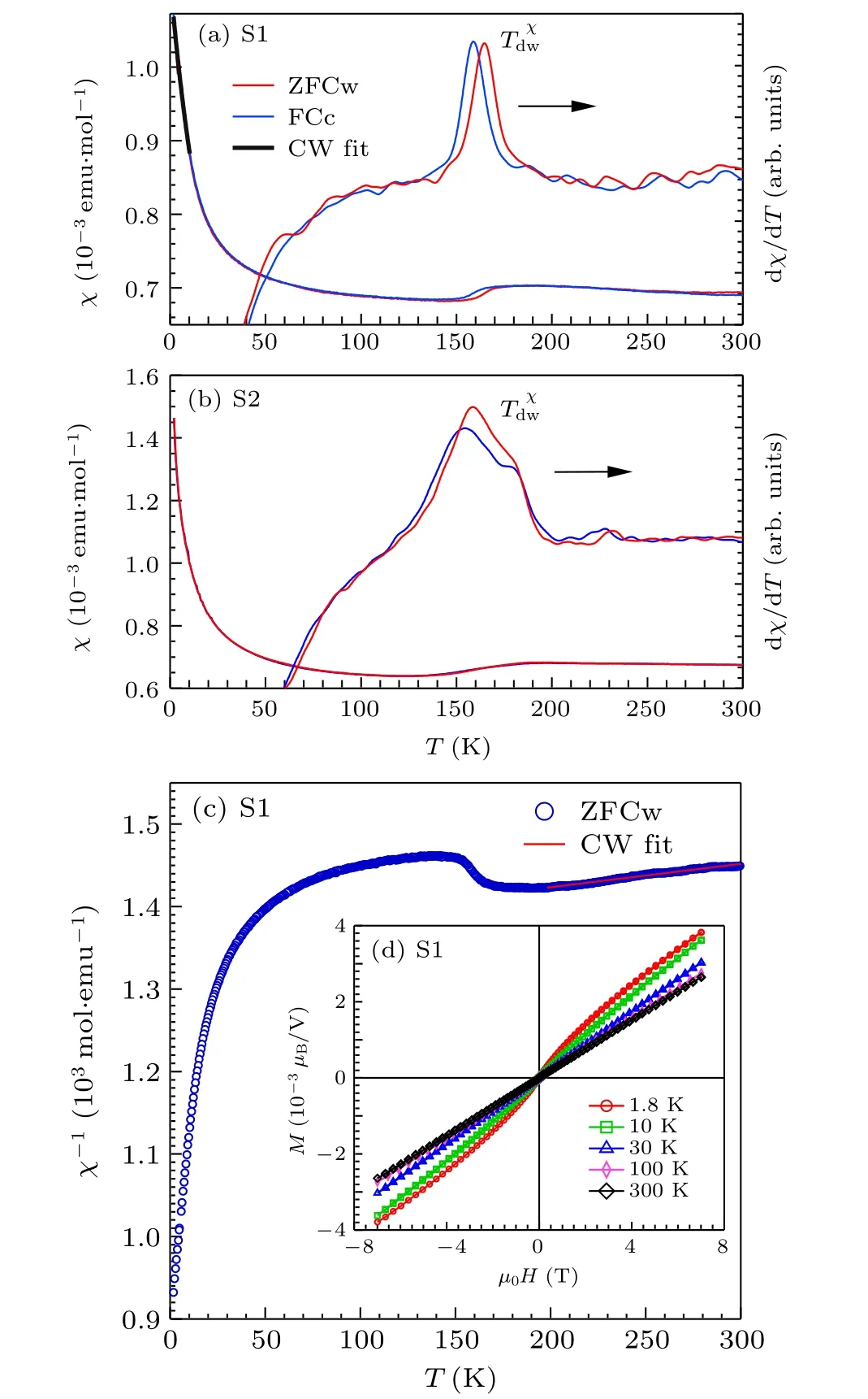
Fig. 3. Temperature dependence of the dc magnetic susceptibility χ(T)and its derivative dχ/dT for V3Sb2 samples: (a)S1 and(b)S2,measured in the ZFCw and FCc modes under an external magnetic field of 1 T.The transition temperature Tχ dw was defined as the peak of the dχ/dT. (c)Temperature dependence of the inverse susceptibility χ-1(T) for sample S1.The CW fitting curves are shown by the solid lines in(a)and(c). (d)The isothermal magnetization M(H)curves for sample S1 measured between+7 T and-7 T at various temperatures.
Figure 3(d) presents the field dependence of magnetizationM(H)for S1 between-7 T and+7 T at various temperatures. TheM(H)curves at all temperatures except for 1.8 K exhibit a linear dependence on the external field with no hysteresis,confirming the absence of ferromagnetic contributions to the magnetism. The magnetic moment of~0.003µB/V at 7 T is small. These results make it significantly different from Fe3Sn2, but similar with theAV3Sb5family where no magnetic order or even local moment of V ion was found.In the isostructural compound Fe3Sn2, the Fe atoms in the kagome plane exhibit strong frustrated magnetic interactions,undergoing complex magnetic phase transitions upon cooling down from a paramagnetic to a collinear ferromagnetic state at 640 K,then to a non-collinear ferromagnetic state at 350 K,and finally to a re-entrant spin glass phase at 70 K.[68]In addition,we find that the magnitudes ofχ(T)andM(H)for V3Sb2are very close to those of KV3Sb5,[37]further indicating the similarity of magnetic states in these two V-based kagome systems.
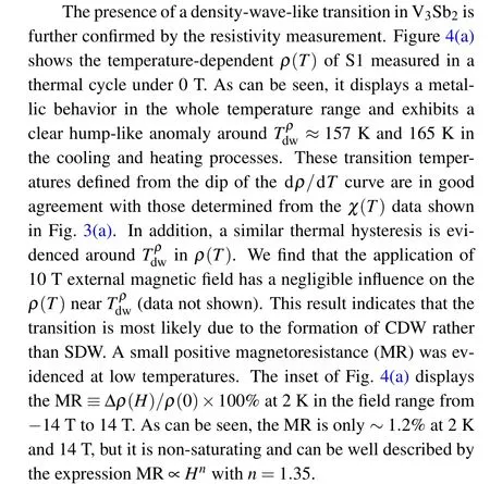
Fig. 4. Temperature dependence of the resistivity ρ(T) and its derivative dρ/dT for the V3Sb2 samples: (a)S1,(b)S2,measured in a thermal cycle under 0 T. The transition temperature Tρ dw was determined from the dip of dρ/dT. Inset of(a)shows the magnetoresistance of S1 at 2 K under fields up to 14 T.
Interestingly, theρ(T) of S2 is quite different with respect to that of S1 as seen in Fig. 4(b). Nonetheless, it also exhibits a pronounced anomaly centered around 150-160 K,and the transition temperatures determined from the minimum of dρ/dTare 152 K and 160 K in the cooling and heating processes,respectively.These temperatures are also consistent with those determined from theχ(T)data shown in Fig.3(b).In comparison with S1,the transition is much stronger and extended over a wider temperature range. In addition,the resistivity belowTdwbecomes higher than that above the transition and displays a clear upturn at low temperatures. These comparisons highlight a better quality of sample S1 than that of S2,and the observed differences might be attributed to the fact that the final sintering temperature of 830°C for S2 is closer to the peritectoid temperature.[55]In the following we thus focus our attention on sample S1. Despite of these differences, the occurrence of density-wave-like transition, most likely a CDW one,aroundTdw≈160 K in V3Sb2should be an intrinsic and bulk behavior.
We have performed variable-temperature powder XRD on S1 from room temperature down to 25 K in order to check if the CDW order is accompanied by obvious structural transition. Within the resolution of our instrument,no obvious peak splitting or satellite peaks are observed in the XRD patterns over the whole temperature range,as illustrated in Fig.5(a)for a portion of the XRD patterns measured at 25 K and 300 K.This indicates that the structural modification,if exists aroundTdw, should be too weak to be detected by our lab XRD, and may await for verification with high-resolution synchrotron XRD or transmission electron microscope at low temperatures. Interestingly, we find that the lattice parameterc(T)exhibits a negative thermal expansion over the whole temperature range, while botha(T) andV(T) display normal contraction upon cooling down as shown in Fig.5(b). The smooth evolution of the lattice parameters acrossTdwis also consistent with the absence of structural transition in V3Sb2.
To further characterize the paramagnetic and metallic ground state of V3Sb2with a possible CDW-like transition,we performed specific-heat measurements on S1 in the wide temperature range. Figure 6 displays theC/Tvs.Tof S1 from 2 K to 250 K under zero field. There is no obvious specific-heat anomaly near the CDW-like transition, suggesting that the thermodynamic signature of this transition is too weak to be observed. We attributed the absence of specificheat anomaly aroundTdwin V3Sb2to the polycrystalline nature of the studied sample.In comparison with the single crystal,the relatively poor crystallization and the presence of grain boundaries in the polycrystalline samples would diminish considerably the specific-heat anomaly around a phase transition.This is well demonstrated inAV3Sb5:[12,37-39]the specificheat anomaly around the first-order transition can be barely observed in the polycrystalline KV3Sb5,[37]while it becomes clearer in the single-crystal KV3Sb5[38]and is much stronger in the CsV3Sb5crystal[12]with a better quality than KV3Sb5.We also noticed that the density-wave-like transition in resistivity and susceptibility of our polycrystalline V3Sb2sample is relatively broad, which can further obscure the thermodynamic signature. The inset of Fig. 6 shows the plot ofC/Tvs.T2at the low-temperature range,and a linear fit toC/T=γ+βT2considering the electronic and lattice contributions yields the Sommerfeld coefficientγ=18.5(1)mJ·mol-1·K-2andβ= 0.73(1) mJ·mol-1·K-4. The Debye temperatureΘD≈237 K can be calculated according to the relationΘD=(12π4nR/5β)1/3, whereR=8.314 J·mol-1·K-1is the ideal gas constant andn=5 is the number of atoms per formula unit. The obtainedγis relatively large compared with elemental metal and is close to that of KV3Sb5,[37]implying the moderate enhancement of the effective electron mass and the presence of electronic correlations.
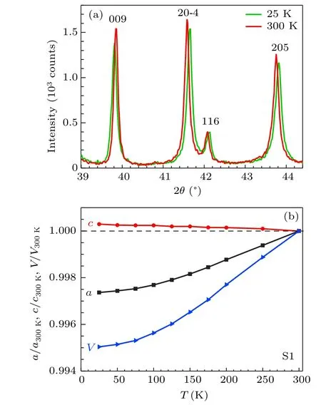
Fig.5. (a)A portion of the XRD patterns measured at 25 K and 300 K.(b) Temperature dependences of the normalized lattice parameters of V3Sb2 sample S1.
From the above characterizations, we can conclude that the bilayer kagome metal V3Sb2is a paramagnetic metal and undergoes a CDW-like transition atTdw≈160 K, which is similar to the family ofAV3Sb5. But no superconductivity was observed in V3Sb2at ambient pressure down to 1.8 K.To explore whether superconductivity emerges after suppressing the CDW under pressure, we measured theρ(T) of S1 under various hydrostatic pressures up to 1.8 GPa by using a piston-cylinder cell. Theρ(T) and its derivative dρ/dTat different pressures are shown in Fig. 7(a). The evolution of the CDW-like transition with pressure can be tracked clearly from the resistivity anomaly. With increasing pressure gradually, the anomaly inρ(T) and the correspondingTdwdetermined from the minimum of dρ/dTcontinuously move to lower temperatures. The pressure dependence of the determinedTdwis plotted in Fig. 7(b). As can be seen,Tdwis suppressed to about 60 K at 1.6 GPa, above which it cannot be clearly distinguished in bothρ(T) and dρ/dT, implying a complete suppression of CDW-like order above 1.6 GPa.However,no sign of superconductivity can be observed down to 1.5 K accompanying the complete suppression of CDWlike order. Whether superconductivity can be realized at much lower temperatures or on high-quality single-crystal samples deserves further studies. Although the above characterizations have revealed a first-order character for the CDW-like transition at ambient pressure, the resistivity anomaly aroundTdwis weakened gradually by applying pressure, Fig. 7(a). If a crossover from first-order to second-order transition can take place, a putative quantum critical point can be realized under pressure. When the high-quality V3Sb2single crystals become available,further high-pressure studies are desirable for in-depth investigations on the pressure-induced quantum critical phase transition.
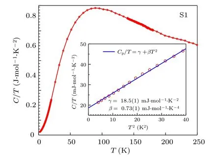
Fig. 6. The C/T vs. T for V3Sb2 sample S1 in the wide temperature range from 2 K to 250 K under zero field. Inset shows the C/T vs.T2 at the low-temperature range, which can be described by a sum of electronic and phonon contributions.
Finally, we calculated the electronic structure of V3Sb2by first-principles calculations. As shown in Fig.8,the V3Sb2shows a metallic nature and its Fermi surface is mainly composed by V’s d orbitals. In V3Sb2, there are two kinds of antimony, which are chemically inequivalent, forming different bands. The hybridization between Sb2 and V is relatively stronger than that between Sb1 and V, because Sb2 are intralayer with V atoms. Meanwhile, we calculated the topological indices of V3Sb2, which arez2w,1=0,z2w,2=0,z2w,3=0 andz4=2, showing a non-trivial topological crystalline property.[61-63]
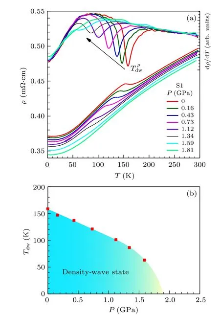
Fig. 7. (a) Temperature dependence of the resistivity ρ(T) and its derivative dρ/dT for the V3Sb2 sample S1 under various pressures up to 1.81 GPa measured with a piston-cylinder cell. (b) Pressure dependence of the density-wave-like transition temperature Tdw.
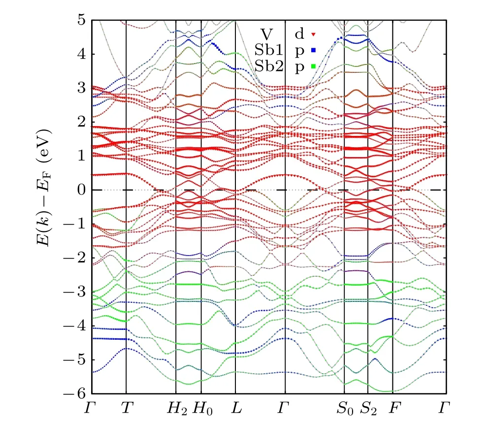
Fig. 8. The projected band structures obtained from DFT calculations for V3Sb2. The orbital characters of bands are represented by different colors and the projected weights are represented by the sizes.
The present work is a preliminary study on the physical properties of V3Sb2polycrystalline samples and leaves many open questions for the future experimental and theoretical studies. For example, electrical transport and magnetic properties at much lower temperatures should be measured to explore possible superconductivity or magnetic order.Low-temperature synchrotron XRD,transmission electron microscope,optical spectroscopy,and scanning tunneling microscope measurements should be performed to elucidate the nature of the density-wave-like transition. Moreover,to acquire high-quality single crystal samples is mandatory for in-depth characterizations of the intrinsic electronic structure by using the angle-resolved photoemission spectroscopy.
4. Conclusion
In summary, we have synthesized the polycrystalline sample of V3Sb2with bilayer kagome lattice of V atoms through a traditional solid state reaction method and characterized its structural, electrical transport, magnetic, and thermodynamic properties via x-ray powder diffraction, resistivity, magnetic susceptibility, and specific heat measurements.We observed no long-range magnetic order in V3Sb2above 1.8 K, which is completely different from the isostructural Fe3Sn2but similar to the kagome metalAV3Sb5(A=K,Rb,Cs)family. In addition,a density-wave-like anomaly was evidenced around 160 K in V3Sb2, making it more similar to theAV3Sb5(A=K,Rb,Cs)family. Moreover,we found that the density-wave-like transition can be gradually suppressed by pressure but no sign of superconductivity can be observed down to 1.5 K. We proposed that V3Sb2is a novel candidate kagome metal to study the interplay between density-waveorder, nontrivial band topology and possible superconductivity.
Note added
During the preparation of this manuscript, we noticed that Shiet al. reported the synthesis and characterizations of the “V6Sb4” single crystal in a recent preprint arXiv:2110.09782.[69]The V6Sb4single crystal was grown at a high temperature of 1100°C and does not exhibit any densitywave-like transition, different from what we observed in the low-temperature phase of V3Sb2in the present work. We attributed the observed different behaviors to the different sintering temperatures.
Acknowledgments
This work is supported by the National Key R&D Program of China (Grant Nos. 2018YFA0305700 and 2018YFA0305800), the National Natural Science Foundation of China (Grant Nos. 12025408, 11874400, 11834016,11921004, 11888101, and 11904391), the Beijing Natural Science Foundation, China (Grant No. Z190008), the Strategic Priority Research Program and Key Research Program of Frontier Sciences of Chinese Academy of Sciences (CAS)(Grant Nos. XDB25000000, XDB33000000 and QYZDBSSW-SLH013), and the CAS Interdisciplinary Innovation Team(Grant No.JCTD-201-01). Work at Oak Ridge National Laboratory was supported by the U.S.Department of Energy,Office of Science,Basic Energy Sciences,Materials Sciences and Engineering Division.
杂志排行

Chinese Physics B的其它文章
- Superconductivity in octagraphene
- Soliton molecules and asymmetric solitons of the extended Lax equation via velocity resonance
- Theoretical study of(e,2e)triple differential cross sections of pyrimidine and tetrahydrofurfuryl alcohol molecules using multi-center distorted-wave method
- Protection of entanglement between two V-atoms in a multi-cavity coupling system
- Semi-quantum private comparison protocol of size relation with d-dimensional GHZ states
- Probing the magnetization switching with in-plane magnetic anisotropy through field-modified magnetoresistance measurement