Instantaneous frequency measurement using two parallel I/Q modulators based on optical power monitoring
2022-01-23ChuangyeWang王创业TigangNing宁提纲JingLi李晶LiPei裴丽JingjingZheng郑晶晶andJingchuanZhang张景川
Chuangye Wang(王创业) Tigang Ning(宁提纲) Jing Li(李晶) Li Pei(裴丽)Jingjing Zheng(郑晶晶) and Jingchuan Zhang(张景川)
1Key Laboratory of All Optical Network and Advanced Telecommunication Network of EMC,Institute of Lightwave Technology,Beijing Jiaotong University,Beijing 100044,China
2Beijing Institute of Spacecraft Environment Engineering,Beijing 100029,China
Keywords: microwave photonics,instantaneous frequency measurement,optical power monitoring
1. Introduction
Instantaneous frequency measurement (IFM) has been a research hotspot in recent years. It has important applications in both military and civil fields, such as radar,communication systems, and electronic warfare systems.[1,2]The traditional electronics method is no longer suitable for future development due to the disadvantages of large loss,small measurement bandwidth and no immunity to electromagnetic interference, but the photonics method perfectly overcomes these shortcomings.[3-5]The researchers have proposed many IFM schemes based on photonics methods, for example,based on the frequency-space mapping method,[6-8]frequency-time mapping method,[9-14]frequency-phase mapping method,[15,16]and frequency-power mapping method.Among them,the method based on frequency-power mapping is the most common. The basic principle is to use a modulator to modulate the received RF signal, then the modulated signal is divided into two channel signals and processed in the optical domain, and the processed optical signals are directly used to measure the optical power, or converted into electrical signals by the photodetector to measure the electrical power. The ACF is constructed to establish the corresponding relationship between the frequency of the RF signal and the power ratio of two channel signals. The frequency of the RF signal can be determined by monitoring the optical power ratio or the electrical power ratio of the two channel signals. In Refs. [17-20], these schemes first used a modulator to modulate the input RF signal, then the modulated signal went through different dispersion processes to achieve different power attenuation,and finally a fixed relationship between the input RF frequency and the power ratio of two output signals was established. The frequency of the RF signal can be derived from the power ratio. In Refs.[21,22],the input RF signal first entered Mach-Zehnder modulator(MZM)for carrier suppression modulation, then the optical filter was used to process the modulated signal, and finally the power ratio of the two processed signals was used to derive the frequency of the input RF signal. In Ref.[23], a phase modulator was put into a Sagnac loop to establish a relationship between the amplitude of the direct current output and the input RF frequency. The measurement range can reach 0.01 GHz-40 GHz and the measurement error is less than 6%. In addition,IFM can also be realized by converting frequency information into power information based on stimulated Brillouin scattering,[24,25]resonators,[26,27]and four-wave mixing.[28]Although these schemes can realize IFM, they are relatively complex in structure. In Ref. [29], the author realized IFM based on a dual-polarization modulator and an electrical delay line. Compared with the previous IFM schemes,the structure is simpler and the cost is lower (there is no expensive highspeed electronic device). However, in this scheme, the polarization controller needs to be accurately kept at 45°, which increases the instability of the system(the polarization device is sensitive to the environment).
In this paper,a simpler structure for IFM is proposed.The scheme only uses one optical source,one electrical delay line,two I/Q modulators and two optical power meters. By setting the bias point of two I/Q modulators appropriately,a fixed relationship between the input signal frequency and the power ratio of two optical signals output by two I/Q modulators is established. The input signal frequency can be derived by the power ratio. The measurement range and measurement error can be adjusted by changing the delay amount of the electrical delay line. The scheme has a better measurement error for low frequency compared with other schemes. The measurement error of low frequency 0 GHz-9.6 GHz can reach-0.1 GHz to+0.05 GHz in simulation.
2. Model and theoretical analysis
Figure 1 shows the schematic diagram of the proposed scheme. The optical signal generated by the CW laser is first divided into two equal power optical signals by an optical power splitter. The two equal power optical signals are injected into two I/Q modulators respectively. I/Q modulator 1 consists of two sub-modulators(MZM-1 and MZM-2),and I/Q modulator 2 consists of two sub-modulators(MZM-3 and MZM-4). The RF signal generated by the RF source is first divided into two equal power electrical signals by an electrical power splitter. One channel electrical signal first passes through an electrical delay line and then is divided by an electrical power splitter, and the generated two electrical signals are injected into the input RF ports of MZM-1 and MZM-3 respectively. The other channel electrical signal passes through an electrical power splitter and the generated two electrical signals are injected into the RF input ports of MZM-2 and MZM-4 respectively. MZM-1,MZM-2,MZM-3 and MZM-4 are biased at minimum transmission point (MITP). I/Q modulator 1 and I/Q modulator 2 are biased at maximum transmission point (MATP) and MITP respectively. Suppose the phase shift induced by DC bias of MZM-1,MZM-2,MZM-3,MZM-4,I/Q modulator 1 and I/Q modulator 2 areφ1,φ2,φ3,φ4,φ5, andφ6respectively, soφ1=φ2=φ3=φ4=φ6=πandφ5=0. The output optical signal by CW laser isEin(t)=E0exp(jω0t), whereE0andω0denote the amplitude and angular frequency respectively. The output electrical signal by the RF source isVRF(t)=VRFcos(Ωt),whereVRFandΩdenote the amplitude and angular frequency respectively. The delay amount of the electrical delay line isτ. The output optical signal of I/Q modulator 1 and I/Q modulator 2 can be expressed as
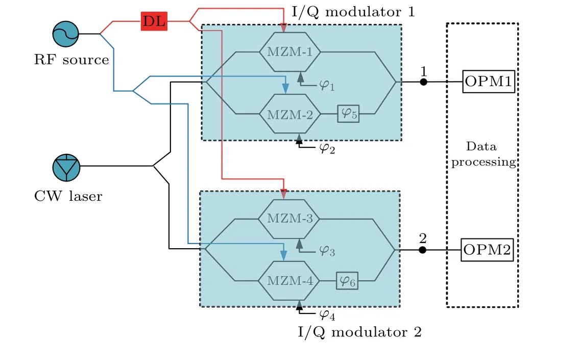
Fig. 1. The schematic diagram of the scheme (RF source: radio frequency source; CW laser: continuous-wave laser; MZM: Mach-Zehnder modulator;DL:electrical delay line;OPM:optical power meter;φ1,φ2,φ3,φ4,φ5,and φ6: phase shifts induced by the DC bias of MZM-1, MZM-2, MZM-3,MZM-4,I/Q modulator 1,and I/Q modulator 2,respectively).

wherefdenotes the frequency of the received RF signal.
According to Eq. (6), whenτis a fixed value, there is a one-to-one corresponding relationship betweenfandP1/P2.Therefore,the frequency of the received RF signal can be derived by the power ratio of two optical signals generated by two I/Q modulators.
Figure 2 is calculated ACF,P1,P2versus RF frequency diagram whenτ=20 ps. Figure 3 is the ACF curve diagram correspondingτ=20 ps, 30 ps, 40 ps, and 50 ps. As can be seen in Fig. 3, different delay amountτcorresponds to different ACF curve. Different ACF curve determines different measurement range.

Fig. 2. Calculated ACF, calculated P1, calculated P2 versus RF frequency when τ =20 ps.
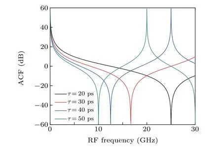
Fig.3. Calculated ACF versus RF frequency when τ =20 ps,30 ps,40 ps,and 50 ps.
3. Simulation and discussion
The feasibility of the scheme is verified by simulation in the software OptiSystem. The parameters are set as follows: the power, wavelength and linewidth of the CW laser are 10 dBm, 1550.12 nm, and 10 MHz respectively. The extinction ratio,insertion loss and half-wave voltage of the MZM are 30 dB, 5 dB, and 4 V respectively. The amplitude of the RF source is 3.6 V (the modulation index of MZM is equal to 1). The electrical delay amount of the electrical delay line is 20 ps. MZM-1, MZM-2, MZM-3 and MZM-4 are biased at MITP. I/Q modulator 1 and I/Q modulator 2 are biased at MATP and MITP respectively. Figure 4 shows simulated received optical power values of the optical power meter 1 and optical power meter 2,and ACF curve when the frequency of RF changes from 0 GHz-30 GHz. As can be seen in Fig. 4,when the frequency of the input RF is from 0 GHz to 25 GHz,the ACF curve is monotonous. There is a one-to-one corresponding relationship between the frequency of the input RF and the value of ACF curve,so we can figure out the frequency of the input RF by the value of ACF in real time.
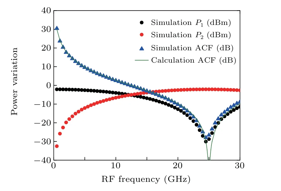
Fig.4. Simulated ACF versus RF frequency when τ =20 ps.
In previous theoretical calculation,the extinction ratio of the modulator is considered to be infinite, but the extinction ratio of the MZM is finite in practice. The effect of extinction ratio of the MZM on the scheme needs to be considered. The extinction ratio of the MZM is set to 20 dB,25 dB,and 30 dB respectively in the OptiSystem. The settings of other parameters remain unchanged. The relationship diagram between ACF and the input RF frequency can be obtained as shown in Fig. 5. Figure 5 shows that the higher the extinction ratio of the MZM is,the closer the obtained ACF curve is to the theoretical ACF curve. This is because the MZM cannot suppress the carrier and even-order sidebands effectively when the extinction ratio of the MZM is not high.
The effect of the modulation index of the MZM on the scheme also needs to be considered. The modulation index of the MZM is set to 0.5,1.0,and 1.5 respectively.The extinction ratio of the MZM is set to 30 dB.Other parameter settings remain unchanged. The relationship diagram between the ACF and the input RF frequency can be obtained as shown in Fig.6.Figure 6 indicates that the larger the modulation indexmis in a certain range, the closer the ACF curve is to the theoretical curve. This is because the amplitude difference between generated first-order optical sidebands and generated higher odd-order optical sidebands by the MZM will increase when the modulation indexmincreases in a certain range, which will reduce the effect of higher odd-order sidebands on the scheme. However,the ACF curves under different modulation index are only different at the end of the monotone interval(0 GHz-25 GHz) and most regions of the monotone interval coincide with the theoretical ACF curve,which indicates that this scheme is not required for the power of the input RF.

Fig. 5. Simulated ACF curve versus input RF frequency when εr =20 dB,25 dB,and 30 dB.
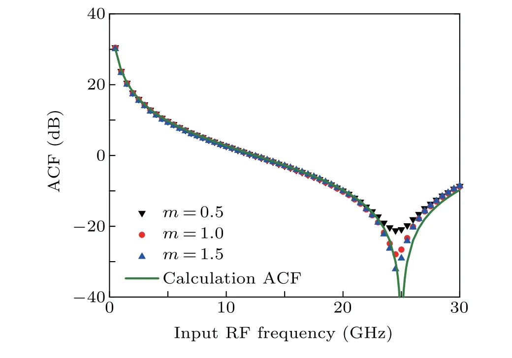
Fig.6. Simulated ACF curve versus input RF frequency when m=0.5,1.0,and 1.5.
When the modulation indexm= 1, the delay amountτ=20 ps and the extinction ratio of the MZM is 30 dB, the estimation error can be obtained as shown in Figs. 7(a) and 7(b). As shown in Fig. 7(a), the simulated frequency measurement results are approximately equal to the calculated frequency measurement results except around 25 GHz. The reason for the larger measurement error around 25 GHz is that the extinction ratio of the MZM is finite. As shown in Fig. 7(b),the estimation error is-0.15 GHz to +0.3 GHz in the measurement range of 0 GHz-24.5 GHz whenτ=20 ps.
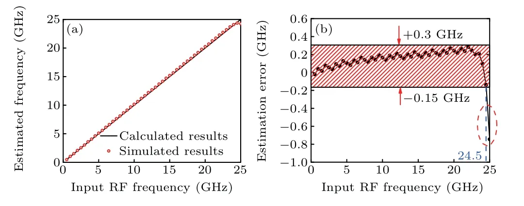
Fig.7.(a)Estimated RF frequency versus input RF frequency.(b)Estimation error versus input RF frequency.
The estimation error is analyzed whenτ=30 ps, 40 ps,and 50 ps. The simulated results are shown in Fig. 8. Figures 8(a) and 8(b) indicate that the measurement range and the measurement error are 0 GHz-16 GHz and-0.3 GHz to+0.05 GHz whenτ=30 ps. The estimation error is larger around 16.7 GHz because the extinction ratio of MZM is finite.Similarly,it can be seen from Figs.8(c)and 8(d)that the measurement range and measurement error are 0 GHz-12.2 GHz and-0.05 GHz to +0.2 GHz whenτ=40 ps. Figures 8(e)and 8(f)indicate that the measurement range and measurement error are 0 GHz-9.6 GHz and-0.1 GHz to+0.05 GHz whenτ=50 ps.
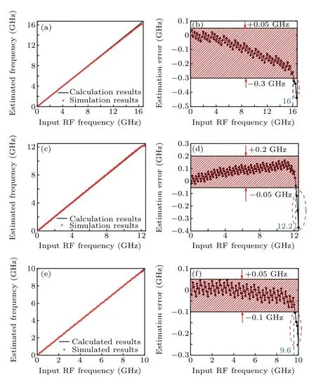
Fig.8.Estimated RF frequency versus input RF frequency at different τ=(a)30 ps, (c) 40 ps, (e) 50 ps. Estimation RF frequency error versus input RF frequency at different τ =(b)30 ps,(d)40 ps,(f)50 ps.
Different measurement ranges and measurement errors are shown in Table 1. There is a trade-off balance between the measurement range and measurement error,as can be seen in Table 1. Whenτincreases, the measurement range decreases,but the measurement error becomes better. Since the ACF curve in this scheme has a high slope at low frequency,the measurement error of low frequency is better than that of other schemes.
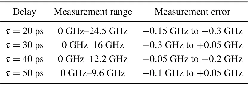
Table 1. Different measurement ranges and measurement errors.
In the scheme, the four sub-modulators are set as MITP.I/Q modulator 1 and I/Q modulator 2 are set as MATP and MITP respectively. The effect of DC bias drift of the MZM on the scheme needs to be considered. Suppose that ΔV/Vπis the DC bias drift of the MZM, where ΔVdenotes the varied amount of DC bias voltage of the MZM andVπdenotes the half-wave voltage of the MZM.Takeτ=50 ps for example. The DC bias drift of MZM-1,MZM-2,MZM-3,MZM-4,I/Q modulator 1 and I/Q modulator 2 are set to±10%respectively. The corresponding parameter settings in the simulation software are shown in Table 2.
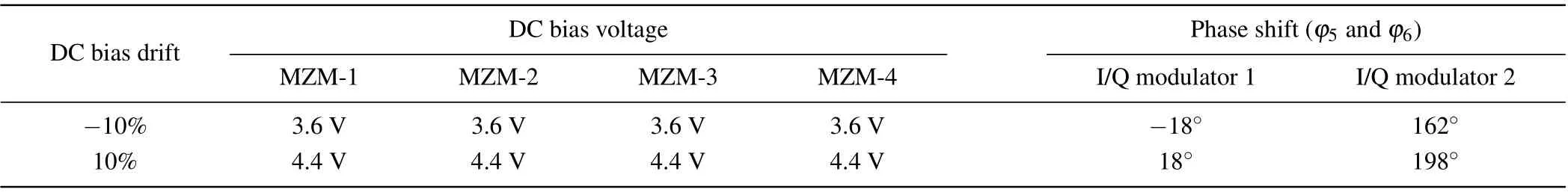
Table 2. Parameter settings for different modulators.

Fig.9. Estimation error diagram when DC bias drift is±10%: (a)MZM-1, (b) MZM-2, (c) I/Q modulator 1, (d) MZM-3, (e) MZM-4, (f) I/Q modulator 2.
Figures 9(a) and 9(b) are the estimation error diagrams when the DC bias drift of MZM-1 is±10% and the DC bias drift of MZM-2 is±10% respectively. As shown in Figs.9(a)and 9(b),the estimation error becomes-0.55 GHz to +0.05 GHz. In order to reach the measurement error(-0.1 GHz to +0.05 GHz) before DC bias drift, the measurement range becomes 0 GHz-6.5 GHz. Figure 9(c) is the estimation error diagram when the DC bias drift of I/Q modulator 1 is±10%. As shown in Fig.9(c),the estimation error becomes-0.7 GHz to+0.07 GHz. In order to reach the measurement error-0.1 GHz to +0.07 GHz, the measurement range becomes 0 GHz-6.5 GHz.
Figures 9(d) and 9(e) are the estimation error diagrams when the DC bias drift of MZM-3 is±10% and the DC bias drift of MZM-4 is±10% respectively. As shown in Figs. 9(d) and 9(e), the estimation error becomes-0.1 GHz to +0.7 GHz. In order to reach the measurement error(-0.1 GHz to +0.05 GHz) before DC bias drift, the measurement range becomes 3.9 GHz-9.6 GHz. Figure 9(f) is the estimation error diagram when the DC bias drift of I/Q modulator 2 is±10%. As shown in Fig. 9(f), the estimation error becomes-0.1 GHz to+0.9 GHz. In order to reach the measurement error(-0.1 GHz to+0.05 GHz)before DC bias drift,the measurement range becomes 3.9 GHz-9.6 GHz.
4. Conclusion
In this paper, a new scheme to realize IFM is proposed.The structure of the scheme is simple; it only consists of one optical source, one electrical delay line, two I/Q modulators,and two optical power meters. By setting each bias point of two I/Q modulators and the delay amount of the electrical delay line properly, a fixed relationship between the frequency of the RF signal and the optical power ratio can be obtained.Since the scheme is carried out in the optical domain, no expensive electronic devices are used. The scheme also has no polarization devices, which reduces the impact of environmental disturbances on the system. The measurement range and measurement error can be adjusted by changing the delay amount of the electrical delay line. Although there exists a trade-off balance between the measurement range and the measurement error,the measurement error of low frequency in this scheme is better than other schemes because the slope of the ACF curve is large at the low frequency. The measurement error in low frequency 0 GHz-9.6 GHz can reach-0.1 GHz to+0.05 GHz. We believe this method will provide guidance for IFM in the future.
Acknowledgments
Project supported by the National Key Research and Development Program of China(Grant No.2018YFB1801003),the National Natural Science Foundation of China (Grant Nos. 61525501 and 61827817), and the Beijing Natural Science Foundation,China(Grant No.4192022).
猜你喜欢
杂志排行

Chinese Physics B的其它文章
- Superconductivity in octagraphene
- Soliton molecules and asymmetric solitons of the extended Lax equation via velocity resonance
- Theoretical study of(e,2e)triple differential cross sections of pyrimidine and tetrahydrofurfuryl alcohol molecules using multi-center distorted-wave method
- Protection of entanglement between two V-atoms in a multi-cavity coupling system
- Semi-quantum private comparison protocol of size relation with d-dimensional GHZ states
- Probing the magnetization switching with in-plane magnetic anisotropy through field-modified magnetoresistance measurement