Three-dimensional vertical ZnO transistors with suspended top electrodes fabricated by focused ion beam technology
2022-01-23ChiSun孙驰LinyuanZhao赵林媛TingtingHao郝婷婷RenrongLiang梁仁荣HaitaoYe叶海涛JunjieLi李俊杰andChangzhiGu顾长志
Chi Sun(孙驰) Linyuan Zhao(赵林媛) Tingting Hao(郝婷婷) Renrong Liang(梁仁荣)Haitao Ye(叶海涛) Junjie Li(李俊杰) and Changzhi Gu(顾长志)
1Beijing National Laboratory for Condensed Matter Physics,Institute of Physics,Chinese Academy of Sciences,Beijing 100190,China
2School of Physical Sciences,CAS Key Laboratory of Vacuum Physics,University of Chinese Acdemy of Sciences,Beijing 100049,China
3Songshan Lake Materials Laboratory,Dongguan 523808,China
4Institute of Microelectronics,Tsinghua University,Beijing 100084,China
5Beijing National Research Center for Information Science and Technology(BNRist),Tsinghua University,Beijing 100084,China
6Department of Engineering,University of Leicester,Leicester LE17RH,UK
Keywords: three-dimensional(3D)vertical ZnO transistor,focused ion beam(FIB),suspended electrodes,the electrical inter-connection in 3D devices
1. Introduction
In recent years, with the rapid development of semiconductor technology, the device size is getting smaller and smaller, which causes many technical challenges and problems,such as high off-state leakage current,the short-channel effect, etc.[1]To solve these challenges, many new materials and architectures have been proposed.[2]Channel materials with high mobility such as GaAs, InGaAs and InAs, exhibit outstanding electron transport properties, which are at the heart of many high-speed and high-frequency electronic systems.[3]Gate oxide materials with high-ksuch as Al2O3and HfO2grown by atomic layer deposition (ALD) possess good interface quality and low gate leakage, which are beneficial for low power consumption.[4]Multi-gate architectures such as fin field effect transistor(FinFET)and gate-all-around(GAA) greatly improve electrostatic control ability over the channel.[5]Among these new architectures,three-dimensional(3D) vertical devices provide a promising solution to overcome the bottleneck of semiconductor technology and improve the performance of traditional two-dimensional(2D)devices. The 3D vertical architecture devices have plenty advantages for future electronic. Firstly, 3D vertical device architectures allow for higher packing density when the devices sizes are the same.[6]Secondly, Yakimetset al.have predicted power savings of 10%-15% for a vertical device layout as compared to a lateral geometry for the 7 nm technology node.[7]Thirdly, the gate length of vertical transistors is no longer determined by lithography, but rather by the thickness of the gate metal film that can be controlled at the nanometer scale during deposition at low cost.[8]There is no doubt that 3D architecture plays a key role in the future integrated circuits. Architectures such as 3D and GAA vertical transistors present attractive approaches to achieving high-density assembly of functional nanodevices. At present, the electrodes of 3D devices are separated by lowkmaterials and connected by contact holes.[9]However, it is cumbersome to fabricate the gate and top electrodes and manage the interconnect layout so as to effectively fabricate 3D vertical devices.[10]Therefore, how to fabricate 3D devices quickly and efficiently is a problem that researchers and manufacturers need to address.Focused ion beam(FIB)technology has shown unique advantages in 3D structure fabrication since it was invented.[11]It can realize accurate structure fabrication at nanoscale, which provides a powerful means for 3D devices fabrication.[12]For example, Pt nanowires deposited by FIB can be used to realize the interconnection between the planar electrode and the 3D top electrode,which greatly simplifies the fabrication processes and shows the advantages of high-density integration of vertical transistors.
In this article,we fabricate a 3D vertical core-double shell structure transistor with ZnO channel and Al2O3gate-oxide,with top suspended electrode and bottom planar electrode interconnected with a Pt nanowire deposited by FIB technology. ZnO and Al2O3are grown by atomic layer deposition(ALD).The fabricated 3D vertical transistors show good electrical characteristic,which indicates the superiority of our 3D interconnect method. In particular,ALD appears very promising due to its atomic level thickness control,relatively low deposition temperature,uniformity over large areas,and wonderful conformality on the 3D structure.[13]The gate oxide and channel materials are not limited to Al2O3and ZnO.
2. Experiments and methods
The detailed fabrication processes of the 3D vertical coredouble shell structure transistor are shown in Fig.1.The heavily boron doped p-type(100)silicon substrate was cleaned by acetone,ethyl alcohol,and deionized water(DW)using an ultrasonic cleaner and dried on the hot plate(Fig.1(a)). Firstly,the electron beam lithography(EBL)and electron beam evaporation (EBE) techniques were used to prepare the Cr hard mask.The diameter and thickness of the Cr mask were 200 nm and 40 nm, respectively (Fig. 1(b)). The photoresist used in this experiment was polymethyl methacrylate(PMMA),which is a positive electron resist and has a high resolution. Secondly,the substrate was put into an inductively couple plasma reactive ion etch system(ICP-RIE)for achieving single Si pillar or arrays with the diameter of 200 nm and the height of 1 µm by a room temperature etching method (Fig. 1(c), RF power: 100 W,ICP power: 1200 W,total pressure: 10 mTorr,SF6:C4F8=45 sccm:40 sccm, etching time: 45 s). Then Cr mask was removed by Cr etchant. Afterwards,50 nm Al2O3and 26 nm ZnO films were grown by ALD at 200°C and 120°C, respectively. Trimethylaluminum (TMA) and DW were selected as the sources of aluminum and oxygen. The thickness of Al2O3deposited at 200°C was 50 nm. After this,180-cycles ZnO film was deposited by ALD as the active layer and the process temperature was 120°C.Diethylzinc(DEZn)and DW were selected as the sources of zinc and oxygen. The thickness of ZnO deposited at 120°C was 26 nm(Fig.1(d)).In the next step, the second EBL process was performed to define the active area,and PMMA as a mask was used to protect vertical channel ZnO. ZnO on other areas was removed by diluted HCl(Fig.1(e)). After this,the EBL and EBE techniques were used again to fabricate planar source(Ti/Al thickness: 10 nm/100 nm)and drain(Al thickness: 150 nm)electrodes. For protecting the channel of ZnO device and forming ohmic contact between ZnO and suspended top electrode,we deposited 50 nm Ti by etch-back method. During this step,we span coat 1.2µm photoresist on the sample,which could coat the total pillar under photoresist. After this,a reactive ion etch system(RIE)was used to thin the photoresist and exposed the ZnO at the top of the pillars(RF power: 200 W,total pressure:10 mTorr,O2=50 sccm,etching time: 90 s). Then,50 nm Ti was evaporated by the thermal evaporation system with tilt angle 15°,which could form the suspended electrode on the top of the silicon pillar arrays after lift-off(Fig.1(f)). After that,another 20 nm thickness TiO film was grown by ALD to protect the channel in the following fabrication step. Tetrabutyl orthotitanate (TTIP) and DW were selected as the sources of titanium and oxygen. Lastly, the 3D Pt nanowire was grown on the planar drain electrode by FIB-CVD technology to directly connect the top suspended drain electrode. During Pt nanowires growth,the substrate was adjusted at fixed rotation angle and tilt angle to keep the FIB imaging to contain the bottom planar electrode and the top suspended electrode in the same direction. Then, the gas precursor molecules were introduced through a gas nozzle and the FIB was operated in“spot mode”, in which the ion beam deflection plates were held at constant potential,the accelerated voltage was 16 keV,the beam current was 1 pA,and the deposition time was 4 min.Finally,single nanopillar or nanopillar arrays device was fabricated as shown in Fig.2.
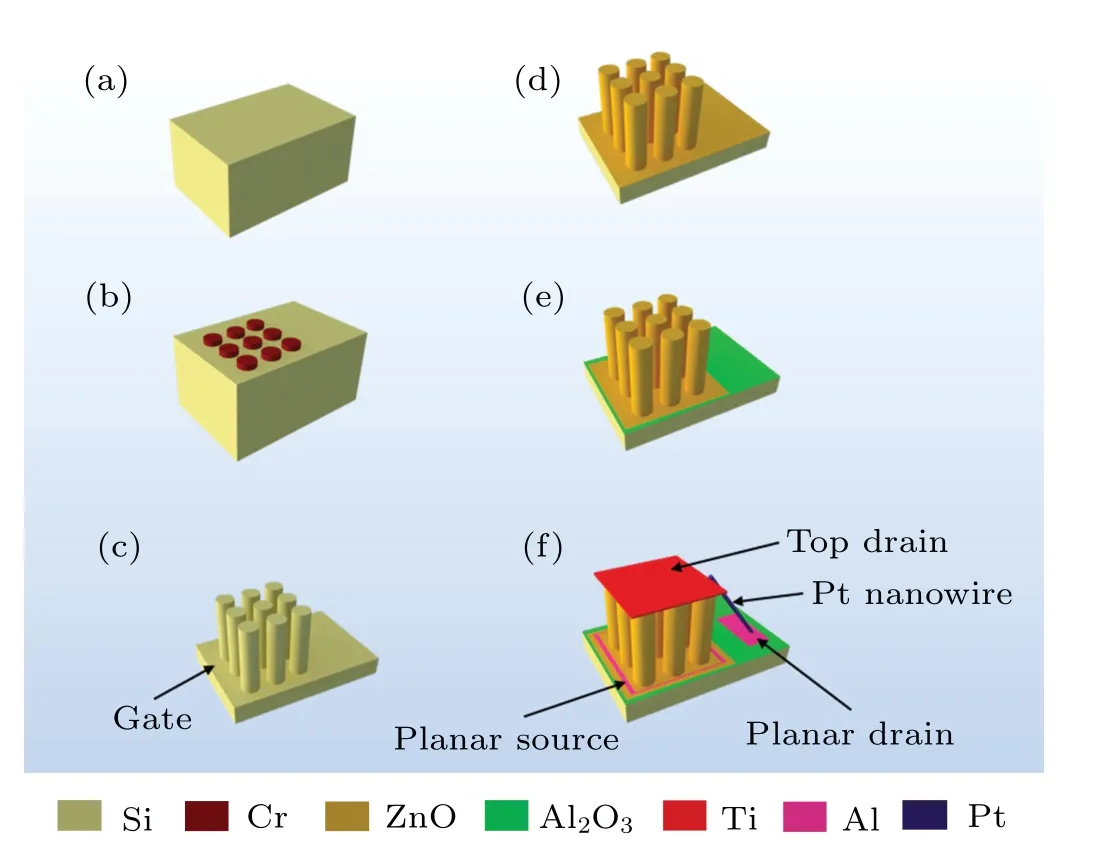

Fig. 2. SEM images of the core-double shell transistors. Side view SEM image of single pillar device(a)and pillar arrays device(b). Top view of single pillar device(c)and pillar arrays device(d).
3. Results and discussion
The performances of 3D vertical devices have been measured with Keithley 4200SCS at room temperature in the dark under air environment. Electrical characterizations of 3D vertical core-double shell transistors with diameter 200 nm and height 1µm pillar are studied below.
Figure 3 shows the source-to-drain current(Ids)as a function of the source-to-drain voltage (Vds) for different sourceto-gate voltage (Vgs) of ZnO 3D transistors with grown temperatures at 120°C. Both the single and arrays core-double shell ZnO devices exhibit typical field-effect transistor characteristics. The channel conductance clearly increases asVdsincreases under positiveVgs, which indicates ZnO grown by ALD is n-type semiconductor,agreeing with all previous studies on ZnO grown by ALD.[14]These devices exhibit a clear pinch-off and saturation,as shown in Fig.3 implying that the ZnO channel can be depleted of free electrons by applying a negative voltage on gate. The carrier concentration of the channel layer influences the conductivity. Therefore, by increasing the grown temperature or annealing device at high temperature, the devices will exhibit a high output current as the conductivity of the channel increases.[15]As we can see from Fig. 2, for the single pillar transistor, the channel width at the planar source side is 1.3 µm and the channel width at the top drain side is 950 nm(of the circumference of a circle with a diameter of 300 nm). For the 2×2 pillar arrays transistor,the channel width at the planar source side is 2.1µm,and the channel width at the top drain side is the circumference of four 300 nm diameter circles,3.8µm. The active region area of the single device is 1.6µm2without the vertical pillar and 2.27µm2with a single vertical pillar,the area of the active region is increased by 41%.For the 2×2 pillar arrays device,the area of the active region is increased by 57% from 4.66 µm2without vertical pillars to 7.33µm2with four pillars. With the increase of pillars number,the vertical active region area will be larger. In an optimal situation,when the cylinder radius isRand the height isH,the cylinder plane area isπR2,the side area is 2πR·H, and the area increase ratio is(2H-R)/R. If the height is 1µm and the radius is 150 nm,the ideal increase ratio is 1233%, which shows the great advantage of high integration of 3D vertical transistors. From Fig. 3, ON-current of the device with 2×2 pillar arrays device is 4.5 times larger than that of the device with single pillar. For the 2×2 pillar arrays device, the channel width at the planar source side is 2.1µm,which is 1.6 times larger than that of the single pillar device,the channel width at the top drain side is 3.8µm which is 4 times larger than that of the single pillar device,however the out-put current of the 2×2 pillar arrays device is 4.5 times larger than that of the single pillar device. In other words,by increasing the number of pillars high out-put current can be achieved, which is beneficial for high density integrated and large ON-current devices.
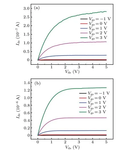
Fig.3. The Ids-Vds characteristics for ZnO-channel 3D transistor with single pillar (a) and 2×2 pillar arrays (b);Vgs steps up from -1 V to 3 V in 1 V increments.
Transistors will show“current crowding”behavior at lowVdswhen the device has a nonohmic source/drain contact,this may be caused by wrong metal contact with active material,or high bulk density of states (DOS).[16]Figure 4 shows the linear region(Vdsfrom 0 to 0.5 V)output characteristics of the ZnO 3D device deposited at 120°C and there is no nonlinear drain current phenomenon. The source/drain contact’s quality of the ZnO 3D device is better evaluated by depicting the derivative of the output curves (dIds/dVds) at lowVdsregion(Vds<0.5 V), which is also shown in Fig. 4. This good behavior demonstrates the high quality of contact between our source/drain electrodes between ZnO.Pt nanowires deposited by FIB could have a good ohmic contact between Al and Ti electrodes, indicating suitability for electrodes interconnection.

Fig.4. Linear region(Vds from 0 to 0.5 V)output characteristics(solid curves)of ZnO 3D devices grown at 120°C.The derivative of Ids versus Vds (dashed curves)is also shown.
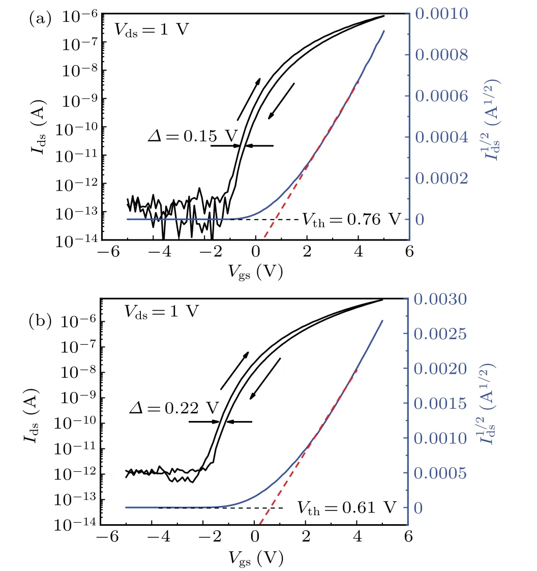
Fig.5. The Ids-Vgs characteristics for ZnO 3D devices with single pillar(a)and 2×2 pillar arrays(b);Vds is constant at 1 V.
The transfer characteristics of ZnO 3D devices are exhibited in Fig.5.Vthcan be extracted by linear fitting forI1/2ds-Vgscurves based on 10% and 90% of the maximumIds.[17]The subthreshold swing(SS)can be calculated using the following equation:

The SS values of 3D core-double shell devices are 300 mV/dec and 340 mV/dec for single pillar device and 2×2 pillar arrays device,respectively. With the increase of pillars,the gate control ability slightly decreases.From Fig.5,theVthof the single pillar device is 0.76 V.As for the 2×2 pillar arrays device,theVthis 0.61 V which is smaller than that of the single pillar device. In thin film transistor, with the decrease of the channel width,carriers in the channel are easier to be captured,which makes the concentration of carriers less under the sameVgsand results in higherVth.[18]This could explain the decrease ofVth.The results show the benefit of 3D vertical architecture transistor, higher channel width and shorter channel length for high integration density and low power consumption.[19]Both devices have large on-off ratio over 106. The representativeIds-Vgshysteresis characteristics of the ZnO 3D devices are shown in Fig.5. The devices show clockwise hysteresis window with 0.15 V for single pillar device and 0.22 V for 2×2 pillar arrays device. This low hysteresis window in both devices indicates that the quantity of traps at ZnO/Al2O3interface or/and within the ZnO channel is small.[20]In other words, during Pt nanowires deposition, gallium ion implantation and damage are negligible by using 1 pA beam current and passivation layer.
4. Conclusion
We present a novel method to fabricate 3D vertical architecture devices. Based on this method, 3D vertical coredouble shell structure transistors were fabricated and characterized. TheI-Vproperties showed significant applied gate voltage dependence,the drain currentIdsincreased as the gate voltage and the number of pillars increased. It also confirmed that electrode contact between the Pt nanowire deposited by FIB and the metal was ohmic contact which would not have adverse impact on the device performance. In addition,during Pt nanowire fabrication,the ion beam did not scan the channel directly so that the current of the ion beam was kept at 1 pA,which made no implantation and damage to the channel material. This new method could simplify the fabrication process for 3D vertical devices whilst maintain the advantages of such devices,i.e.,high integration density,low power consumption,and so on.
Acknowledgements
Project supported by the National Key Research and Development Program of China (Grant Nos. 2016YFA0200400 and 2016YFA0200800), the National Natural Science Foundation of China (Grant Nos. 61888102, 12074420, and 11674387), Strategic Priority Research Program of the Chinese Academy of Sciences (Grant No. XDB33000000), and Key Research Program of Frontier Sciences,Chinese Acdemy of Sciences(Grant No.QYZDJ-SSWSLH042).
猜你喜欢
杂志排行

Chinese Physics B的其它文章
- Superconductivity in octagraphene
- Soliton molecules and asymmetric solitons of the extended Lax equation via velocity resonance
- Theoretical study of(e,2e)triple differential cross sections of pyrimidine and tetrahydrofurfuryl alcohol molecules using multi-center distorted-wave method
- Protection of entanglement between two V-atoms in a multi-cavity coupling system
- Semi-quantum private comparison protocol of size relation with d-dimensional GHZ states
- Probing the magnetization switching with in-plane magnetic anisotropy through field-modified magnetoresistance measurement