Pure spin-current diode based on interacting quantum dot tunneling junction*
2021-11-23ZhengzhongZhang张正中MinYu余敏RuiBo薄锐ChaoWang王超andHaoLiu刘昊
Zhengzhong Zhang(张正中) Min Yu(余敏) Rui Bo(薄锐)Chao Wang(王超) and Hao Liu(刘昊)
1Faculty of Mathematics and Physics,Huaiyin Institute of Technology,Huaian 223003,China
2The Affiliated Drum Tower Hospital of Nanjing University Medical School,Nanjing 210093,China
Keywords: pure spin current,semiconductor quantum dot,spin diode
1. Introduction
Control of the charge and spin in electric devices is an interesting theme, which is experiencing a burst of activity.[1,2]Generally,electronic devices control the charge current,which is the flow of electrons and generates Joule heat. With the development of integrated circuits and the molecularization of electronic devices, the energy consumption of electronic devices will increase. Spintronics may provide a feasible way to reduce heat generation in nanoscale devices.[3,4]In most cases, the charge current can be calculated as the sum of the currents of spin-up and spin-down electrons, while the spin current is the difference between them. If both charge and spin currents coexist, then the current is called a spin-polarized current. When equal amounts of spin-up and spin-down electrons travel in opposite directions, which results in the net charge through the device being zero and the spin current having a finite value, the pure spin current phenomenon appears.[5-10]To date, many studies have been proposed to obtain a pure spin current,[11-13]such as the spin Hall effect,[14,15]and spin-Seebeck effect,[16,17]and spinphotogalvanic effect.[18-20]Some designs have been successfully implemented experimentally,for example,in a quantum wire based on GaAs/AlGaAs heterostructures.[21,22]In these devices,the spin current can be obtained and detected by using a quantum point contact(QPC)electrode or coupled quantum dots(QDs),which does not rely on optical equipment,a magnetic material, or spin-orbit interactions and can be facilely controlled by an electrical method in experiments.
Regarding the charge degree of freedom, an important device in modern electronics is the diode: a charge current can flow through it under a forward bias, but the current is very small under a reverse bias. To date, various diodes have been successfully manufactured, and they have been extensively used in almost all electronic products and instruments.[23]In general, a diode controls the flow of charge in circuits. Very recently, the spin-current diode,[24-27]which is a counterpart to the traditional chargecurrent diode regarding the spin degree of freedom, has been extensively studied in recent years concerning its potential application in spintronics and quantum information. Many spincurrent diodes in low-dimensional systems,such as a stanene nanoribbon,[28]monoaxial chiral magnets[29]or a lead/FM semiconductor/lead heterojunction,[30]have been theoretically proposed. In these systems, the spin current flows only in one spin bias direction, and the net charge through the junction is tiny. Furthermore, it has been mentioned in Ref. [30]that the effect of the spin diode can be extended to a leadferromagnetic QD-lead structure. Inspired by these works, it is expected that nanostructures based on QDs can also be designed as a spin diode devices which is independent of charge current.
In this work,we propose a novel type of pure spin-current diode based on a single interacting ferromagnetic QD sandwiched between a pair of nonmagnetic electrodes. Similar to the experimental work in reference,[21]a spin bias can be applied via the left QPC electrode, and a spin current will tunnel through and be controlled in the QD-based tunneling junction.[31,32]We focus on the regime where sequential tunneling dominates transport, and the system can be described in terms of a generalized master equation with transition rates obtained via a real-time diagrammatic approach. Our numerical results show that a pure spin current will always emerge in a certain gate voltage regime, regardless of whether the Coulomb repulsion energy exists. More interestingly,the pure spin current exhibits asymmetricIS-VScharacteristics. Such asymmetry in the spin current suggests diode-like behavior with respect to the spin bias,which can be switched by changing the external magnetic field. Unlike the traditional chargecurrent diode, the ability to control the polarity direction of the spin current is a great advantage. Note that for the chargecurrent diode(e.g.,p-n junction),its polarity direction is fixed and cannot be changed once the device is fabricated.
2. Model and Hamiltonian
As shown in Fig.1,the system we consider here consists of a single interacting QD sandwiched between a couple of nonmagnetic electrodes. The Hamiltonian of the system can be written as[33-36]

The spin-σcurrent flowing through the QD can be written asIσ=(ILσ −IRσ)/2 and scaled byeΓ0/¯h. Then, the total spin current and charge current flowing through the system can be calculated by the formulasIS=I↑−I↓andIC=I↑+I↓.

Fig.1. Model setup: (a)illustration showing a possible realization of a QDbased spin diode device employing one QPC lead and one nonmagnetic lead with a spin bias applied across the junction. (b)Schematic energy diagram of the device with an external magnetic field applied on the dot.

3. Result and discussion
First, we demonstrate the pure spin-current diode effect in this junction without the intradot Coulomb interaction(U=0 meV).As shown in Fig.2(a),we studied the spin currentISas a function of spin bias and gate voltage with field-induced Zeeman splitting ∆H=0.2 meV and equilibrium temperatureT=1 K. The spin current spectrum can be divided into two parts. In the gate voltage windows far from theεd=0 point,for example,εd≫0.1 meV orεd≪−0.1 meV,symmetry of theISchange can be seen with respect to the spin bias direction. In these regions, the device does not have spin diode features. However, if the QD level lies in the regime close to theεd=0 point, for example,−0.1 meV<εd<+0.1 meV,then an asymmetry in spin currentISwith respect to the spin bias is typically observed. On the other hand,the charge currentICin Fig. 2(b) can also be divided into two parts: In the gate voltage windows far from theεd=0 point,symmetry and a nonzero distribution ofICcan be seen with respect to the spin bias. However,if the QD level lies in the regime close to theεd=0 point, for example,−0.1 meV<εd<+0.1 meV,then the charge current completely vanishes, which indicates that equal amounts of spin-up and spin-down electrons tunnel through the junction in opposite directions,i.e.,pure spincurrent diode behavior occurs.To further examine this anomalous suppression for the pure spin current,we display theISVScharacteristics at gate resonance voltageεd=0 meV. As shown in Fig.2(c),it is obvious that the spin currents can flow easily from the QPC (left) lead to the NM (right) lead with a positive spin biasVS>0, while these flows are suppressed for the opposite directionVS<0. With a decrease in equilibrium temperatureT, the spin current for a forward spin bias increases, whereas the reverse one decreases, and the diode feature is gradually enhanced, as shown in Fig. 2(c). However, regardless of how the equilibrium temperature changes,the tunneling charge currentICis always suppressed to zero,which means that this QD structure can always function as a pure spin-current diode in the gate resonance voltageεd=0 regime.

Fig. 2. (a) Spin current and (b) charge current as a function of spin bias and gate voltage in the absence of the Coulomb interaction with equilibrium temperature T =1 K. (c) Spin current and charge current variations with spin bias with a fixed gate voltage εd =0, and (d)rectification ability variation with gate voltage under different equilibrium temperatures with spin bias VS=±1.5 mV.
To understand the underlying physics, we give a simple analysis of the spin current and charge current under some approximations.For the intradot Coulomb interactionU=0,the energy level of the spin-up(down)state isε↑(↓)=εd±∆H/2.By using the rate equation we mentioned in Section 2, if we define
then the charge current can be obtained as

Here,

Obviously, from Eq. (5), we can see that regardless of how other parameters change,the charge current is always fixed at zero when the gate voltage is given at theεd=0 point. However,at this gate voltage point,the spin current yields
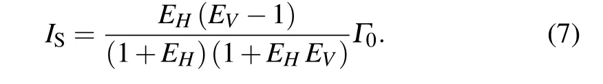
If the temperature is extremely low(T →0),then equation(7)can be approximated as
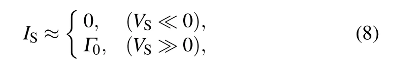
which indicates that a perfect spin-current diode without any electron charge tunneling through it can be present under low equilibrium temperature conditions.
To investigate the spin current rectification ability in this device, we plot the rectification coefficientRSas a function of gate voltage with a spin biasVS=±1.5 mV in Fig. 2(d).If the gate voltage is set far from the regime of [−∆H/2<εd<∆H/2],then the coefficientRSis equal to 0,which means that no rectification occurs in these regimes. In contrast, if the gate voltage lies within this window,thenRSquickly rises to a finite value depending on the equilibrium temperatureT.According to Eq. (7) and Eq. (8), if given an extremely low equilibrium temperature and a positive Zeeman splitting energy, thenRScan reach up to 1, which represents a perfect spin-current diode device.
Thus far,we have considered cases in which the Coulomb repulsion energy in the QD is extremely small. Next,we generalize this pure spin-current diode effect to a regime of a finite Coulomb repulsion energy in this device. As shown in Figs.3(a)and 3(b),we studied the spin currentISand charge currentICas a function of spin bias and gate voltage, with temperatureT=1 K and intradot Coulomb interactionU=10 meV,corresponding to the real experimental conditions.[38]Similar to the diode effect we discussed in relation to Fig. 2,the charge current can also be divided into two parts. In the gate voltage windows ofεd≫0 orεd≪−U, symmetry of the charge current changes can be seen with respect to the direction of the spin biasVS. In these regions, a pure spin current phenomenon does not exist because of theIC̸=0. However, if the QD level lies in the Coulomb blockade regime,i.e.,−10 meV<εd<0 meV,then the net charge through the junction rapidly decreases to zero. More interestingly, compared to the spin diode effect studied in Fig.2,the spin current tunneling through the junction with a finite Coulomb repulsion energy is quite different. In Fig.3(a), we can see that in two small gate voltage windows,i.e.,[−10.1,−9.9]meV and[−0.1,0.1] meV, obvious asymmetry of theISchange can be observed with respect to the spin bias direction. Because the charge current only decays to zero in the Coulomb blockade regime, the pure spin-current diode effect can be detected in the parts overlapping with these gate voltage windows,i.e.,[−10,−9.9] meV and [−0.1,0] meV. In Fig. 2(c), we plot theIS-VScharacteristics in these gate voltage regimes. It is obvious that the spin currents can flow easily from the left lead to the right lead with a positive spin biasVS>0, while these flows are suppressed for the opposite directionVS<0.With a decrease in equilibrium temperatureT, the spin current for a forward spin bias increases, whereas the reverse one decreases,and the diode feature is gradually enhanced,as shown in Fig.3(c). Furthermore,compared with Fig.2(c),the suppression effect of spin current under a negative spin bias regime with a finite temperature seems to be stronger due to the existence of Coulomb repulsion energy. This means that the Coulomb repulsion energy in QD structure under real experimental conditions will be beneficial to the discovery of this phenomenon.
To investigate the spin current rectification ability,we also investigated the rectification coefficientRSas a function of gate voltage with a spin biasVS=±1.5 mV in Fig.3(d). If the gate voltage is set far from the Coulomb repulsion regime,i.e.,εd≫0 orεd≪−U,then the coefficientRSis equal to 0,which means that no rectification occurs in these regimes.In contrast,if the gate voltage lies within the window ofεd∈[−U,0],thenRSquickly rises to a finite value depending on the equilibrium temperatureT. If an extremely low equilibrium temperature and a positive Zeeman splitting energy are given,thenRScan reach 1, which means that a perfect spin-current diode effect is robustly maintained and does not depend on whether the Coulomb repulsion energy exists.
To understand the physical mechanism behind Fig.3,we plot a schematic diagram of the electron tunneling process in this QD-based junction. In the presence of a Coulomb repulsion energy on the QD,there are a total of four electron transmission channels in the system, with two for spin-up states and the other two for spin-down states(see Figs.1 and 4). For ease of discussion, we assume that the equilibrium temperature is very low (T →0 K). If we apply a positive spin biasVS>0, then equal amounts of spin-up and spin-down electrons will tunnel through this junction in opposite directions in two resonance voltage regimes,[−∆H/2−U,∆H/2−U],and[−∆H/2,∆H/2],as shown in Figs.4(a)and 4(b).In these two regimes,the spin current can flow easily from the left lead to the right lead, and the device switches “on”. In contrast,if the device works in the negativeVSdirection,then a downspin electron will be trapped in the QD due to the positive Zeeman splitting energy and negative spin bias voltage in the Coulomb blockade regime.Neither a spin current nor a charge current can tunnel through the device easily in this gate voltage regime,and the device switches“off”.Therefore,a perfect pure spin current diode can only be found in the gate voltage region where the two phenomena coexist,i.e.,the gate voltage windows[−U,∆H/2−U]and[−∆H/2,0].
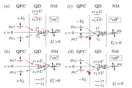
Fig.4. Schematic diagram of the electron tunneling process for(a)[(b)]the forward spin bias and (c) [(d)] backward spin bias directions, with a positive Zeeman splitting ∆H >0 and the gate voltage tuned in the windows of[−∆H/2−U, ∆H/2−U]and[−∆H/2, ∆H/2].

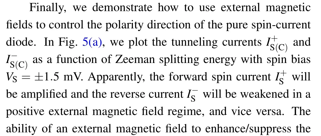
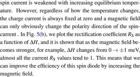
Fig.5. (a)Forward(or reverse)spin current or charge current and(b)rectification coefficient RS as a function of the external magnetic field,with gate voltage εd=0 meV and U =0 meV.
4. Conclusion
In conclusion, we have proposed a pure spin-current diode device based on a single quantum dot weakly coupled to one QPC lead and one NM lead. By tuning the gate voltage to certain windows,we observed a clear asymmetry in the spectrum of spin currentISas a function of spin bias,regardless of whether the Coulomb repulsion energy was present. Our analysis shows that the performance of the spin-current diode depends on the competition between the external magnetic field and the equilibrium temperature. More interestingly, by adjusting the magnetic field, we can change the polarity of the spin-current diode or enhance its rectification ability performance. The numerical results in this device scheme are based on the real experimental environment,which can be easily fabricated and realized with current technology.
猜你喜欢
杂志排行
Chinese Physics B的其它文章
- Numerical investigation on threading dislocation bending with InAs/GaAs quantum dots*
- Connes distance of 2D harmonic oscillators in quantum phase space*
- Effect of external electric field on the terahertz transmission characteristics of electrolyte solutions*
- Classical-field description of Bose-Einstein condensation of parallel light in a nonlinear optical cavity*
- Dense coding capacity in correlated noisy channels with weak measurement*
- Probability density and oscillating period of magnetopolaron in parabolic quantum dot in the presence of Rashba effect and temperature*