Non-inverting buck-boost DC-DC converter based on constant inductor current control
2021-07-13YaoSuyiJiangJianguo
Yao Suyi Jiang Jianguo
(School of Electronic Information and Electrical Engineering, Shanghai Jiaotong University, Shanghai 200240, China)
Abstract:The hysteresis control combined with PWM control non-inverting buck-boost was proposed to improve the light load efficiency and power density. The constant inductor current control (CICC) was established to mitigate the dependence on the external components and device variation and make smooth transition between hysteresis control loop and pulse width modulation (PWM) control loop. The small signal model was deduced for the buck and boost operation mode. The inductor current slope control (ICSC) was proposed to implement the automatic mode transition between buck and boost mode in one switching cycle. The results show that the converter prototype has good dynamic response capability, achieving 94% efficiency and 95% peak efficiency at full 10 A load current.
Key words:four switch buck-boost converter; inductor current slope control; constant inductor current control; small signal model
Battery is the most extensive use power supply in most applications, including electronic devices (mobile phone, wearable devices, etc.), automotive infotainment and start-stop system[1-2]. Battery voltage can be either greater or lower than the system operation voltage no matter it is charged or discharged. Thus, the implementation of non-inverting buck-boost converters is critical for regulating purpose. Compared with Sepic, Zeta and Flyback, four-switch buck-boost has much lower switch stress and magnetic element power loss, resulting in better EMI performance and higher power density. The traditional non-inverting buck-boost employs four switches with three-mode control to realize the up-down transition. However, since the hysteresis ΔVis introduced to avoid the fluctuation of the duty cycles, the line regulation performs not good enough when input voltage is close to output voltage[3]. Even with the compensation technique[4]or extra circuit like PLL[5], the dead zone still exists and the output voltage drops as the input voltage changes. The hybrid feed-forward control scheme[6-7]improves the line transient performance but needs input voltage sensing, one more dynamic sawtooth generator[8]and PWM comparator, which together make the system control more complicated[9]. Although hysteresis control could improve the efficiency in light load and load step response, the transition between hysteresis mode and PWM mode is not smooth or accurate due to the variation of external component parameters. The tradition hysteresis mode relies on the two non-overlap thresholdsILH(load current from PWM to hysteresis) andILP(load current from hysteresis to PWM)[10]. The buck converter usually senses the inductor current as the load current and makes the decision by comparing with a reference current threshold. However, the inductor current of boost and buck-boost is related to theVinandVo. This paper proposes a constant inductor current control (CICC) method to make the operation mode transition smooth between hysteresis control mode and PWM control mode. Compared with the fixed transition current threshold, the CICC scheme decouples from the input and output voltage change and the parameter variation of external components.
In this paper, an inductor current slope control (ICSC) method is proposed to transit the operation mode between buck and boost in one switching cycle automatically so that it can mitigate both overshoot and undershoot of the output voltage when the input voltage changes.
1 System Architecture
The proposed buck-boost loop control architecture is composed of the hysteresis control loop and PWM control loop shown as Fig.1. The hysteresis control loop is effective during light load while the converter transits to PWM control loop when the load increases. In hysteresis loop control, the CICC control block makes inductor current (IL) operate between the peak current limit (Ip) and the zero current (IZC) until the output voltage (Vo) exceeds the rising threshold of the feedback hysteresis comparator (FHC). Then the converter works from the alive state to the sleep state, dramatically saving the controller loss and switching loss, and obviously improving the efficiency in light load condition. With the average inductor current ramping up, the valley inductor current increases gradually more than the zero current (IZC), leading to the converter transition from hysteresis mode to PWM mode. The CICC is proposed to make the peak to valley inductor current operate with a constant value asIp, so that the control scheme can easily implement the smooth transition between hysteresis control loop and PWM control loop. The efficiency dip is eliminated at the mode transition point, compared with the traditional fixed inductor current transition threshold.
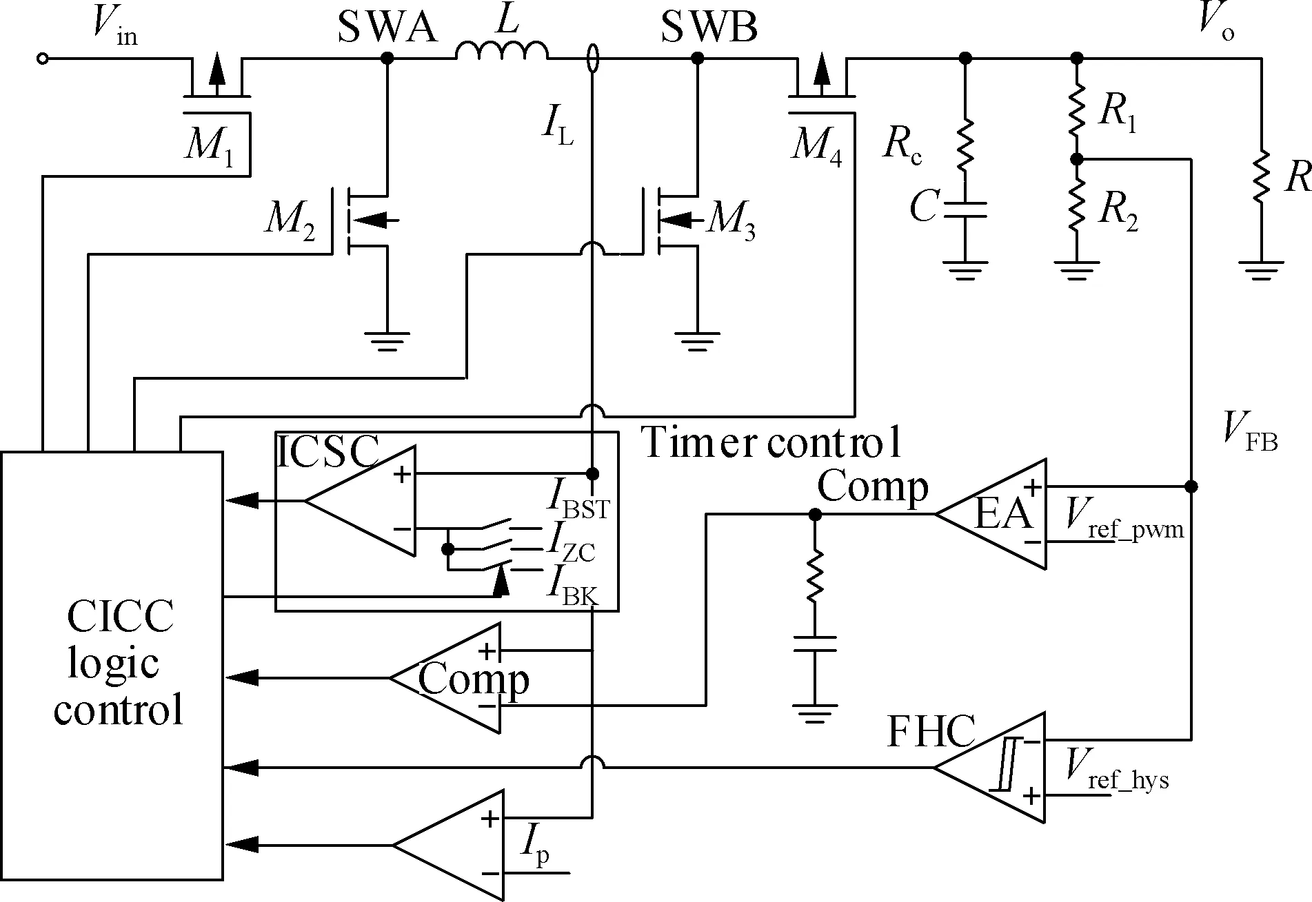
Fig.1 The novel buck-boost control diagram
Both in hysteresis and PWM control, ICSC block sensesIL. With a given inductor, the slope ofILis in proportion to the voltage across the inductor. (Vin-Vo)/Lis the common coefficient in buck-boost mode so that it can be a uniform input as the current slope comparator which determines the boost or buck mode in one switching cycle. ICSC can greatly improve the line regulation performance and improve the efficiency when theVinis close toVo.
2 System Implementation
2.1 Inductor current slope control (ICSC)
The state machine transition diagram of Fig.2 shows the operation principle of ICSC. At the initial state, assuming thatVois greater than the reference of the feedback hysteresis comparator (FHC), the converter is operating in the sleep state S1 with all switches off which are shown in Tab.1. When the output signal of FHC turns to low, the converter transits to buck mode S3, in which M1 and M4 are turned on, ifVinis greater thanVo. WhenILexceedsIp(PK=1), the converter transits to mode S4, in which M2 and M4 are turned on. UntilILis equal to the zero current (ZC=1), the converter transits back to mode S3. As long as the FHC andCBSTkeep low,ILramps up and down between zero current (IZC) andIp. TheCBSTis the output signal of the boost mode comparator with two inputs as of inductor current and boost mode current thresholdIBST, as shown in Fig.3. WhenVFBis higher than reference voltageVREF_HYS, FHC goes high and the converter transits back to the sleep state S1.
WhenVinbecomes lower thanVoin S1 or S4 under buck mode, the converter changes to boost mode immediately in state S3 if onlyILis lower than the boost mode current thresholdIBSTat the delayTBST, since the rising slope ofILis proportional toVin-Voand can be inferred as theVinandVorelative level. When theVinturns lower thanVoafter the delayTBSTbut beforeILhitsIp, the extra check at delayTBST1is to assure that the converter changes to boost mode. At delayTBST1, ifILis still lower thanIp, the comparator outputCBST1transits to high and M1 is turned off. The converter changes to boost mode in the next switching cycle.
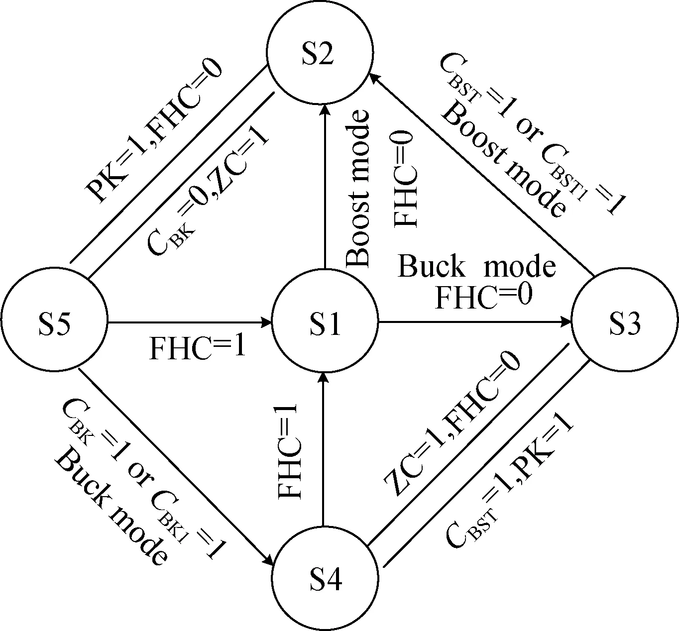
Fig.2 ICSC operation state machine
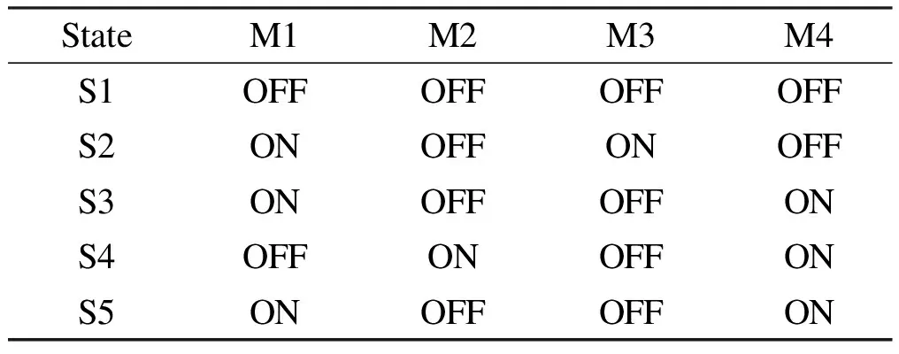
Tab.1 ICSC control scheme
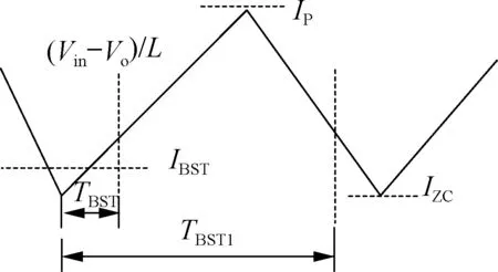
(b)Fig.3 Mode transition of inductor slope control. (a) Buck mode; (b) Boost mode
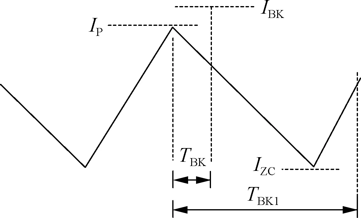
Under boost mode, the converter operates between S2 and S5 asILramps up and down between the peak currentIpand zero current (IZC), if only FHC andCBKkeep low.CBKis the output of the buck mode comparator, with two inputs as of the inductor currentILand the buck mode current thresholdIBK. IfVinbecomes higher thanVoin S1 or S2, it transits to the buck mode immediately in state S5 whenILis higher thanIBKat the delayTBKsince the falling slope ofILis proportional toVo-Vinand can be inferred as theVinandVorelative level. IfVinbecomes higher thanVoafter the delayTBKbut beforeILhitsIZC, the extra check at delayTBK1is to assure that the converter changes to buck mode as well. At delayTBK1, ifILis still higher thanIZC, the comparator outputCBK1transits to high and M4 is turned off. WhenVFBis higher than the reference voltageVREF_HYS, FHC goes high and the converter transits back to the sleep state S1.
Based on the control scheme analysis, these transitions of the operation mode are all completed in one switching cycle with ICSC control. Furthermore,Vois charged up quickly and the converter goes to sleep state automatically as the IL slope is flat and theIpis much larger than the load current. Therefore, compared with the conventional buck-boost without operation mode detection, there is no efficiency degraded whenVinis close toVo.
The mode transition threshold ofVinandVolevel can be expressed as
(1)
(2)
As voltage drops in M1~M4, it is necessary to set the mode transition threshold forVinslightly higher thanVo. The boost-to-buck threshold is larger than the buck-to-boost threshold to avoid glitches during mode transitions.
2.2 Constant peak and valley inductor current control
CICC is proposed as the constant peak and valley inductor current control scheme. It is not an external component dependent control scheme that can smoothly and accurately transit between hysteresis loop and PWM loop. In order to improve the efficiency and transient performance, the hysteresis control loop is more effective with light load. The inductor current ramps up and down betweenIpand zero current untilVoexceeds the hysteresis window and then the converter goes into sleep mode to reduce the switching loss and controller loss. With the increase in the load current,VoandVFBdrops gradually as the inductor current from peak to valley is constant. Meanwhile, the compensation node voltage of error amplifier increases to enlarge the load capability and PWM control loop is effective on the output regulation after 32 clock cycles. Finally, the reference voltage of hysteresis control and PWM control are adjusted simultaneously to cancel the load regulation under different control modes. Fig.4 shows the control loop transition from hysteresis to PWM.
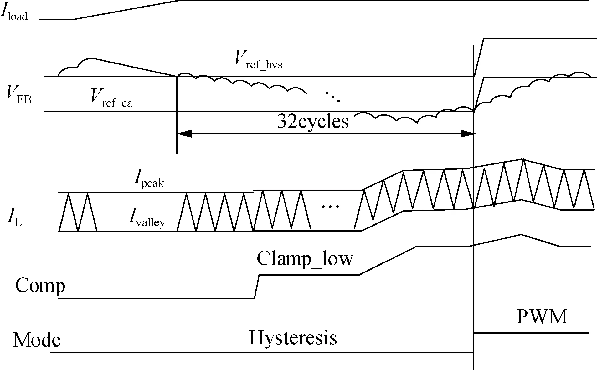
Fig.4 Hysteresis to PWM mode transition of CICC
Similarly, the inductor current and compensation node voltage decrease as the load current decreases. The converter starts to skip switching pulses whenVFBgoes higher thanVREF_HYSas the inductor current from peak to valley is constant. Meanwhile, the compensation node voltage of the error amplifier decreases and the hysteresis control loop is effective on the output regulation after 8 burst cycles. Finally, the reference voltage of hysteresis control and PWM control are adjusted simultaneously to cancel the load regulation under different control modes. Fig.5 shows the control loop transition from PWM to hysteresis mode.
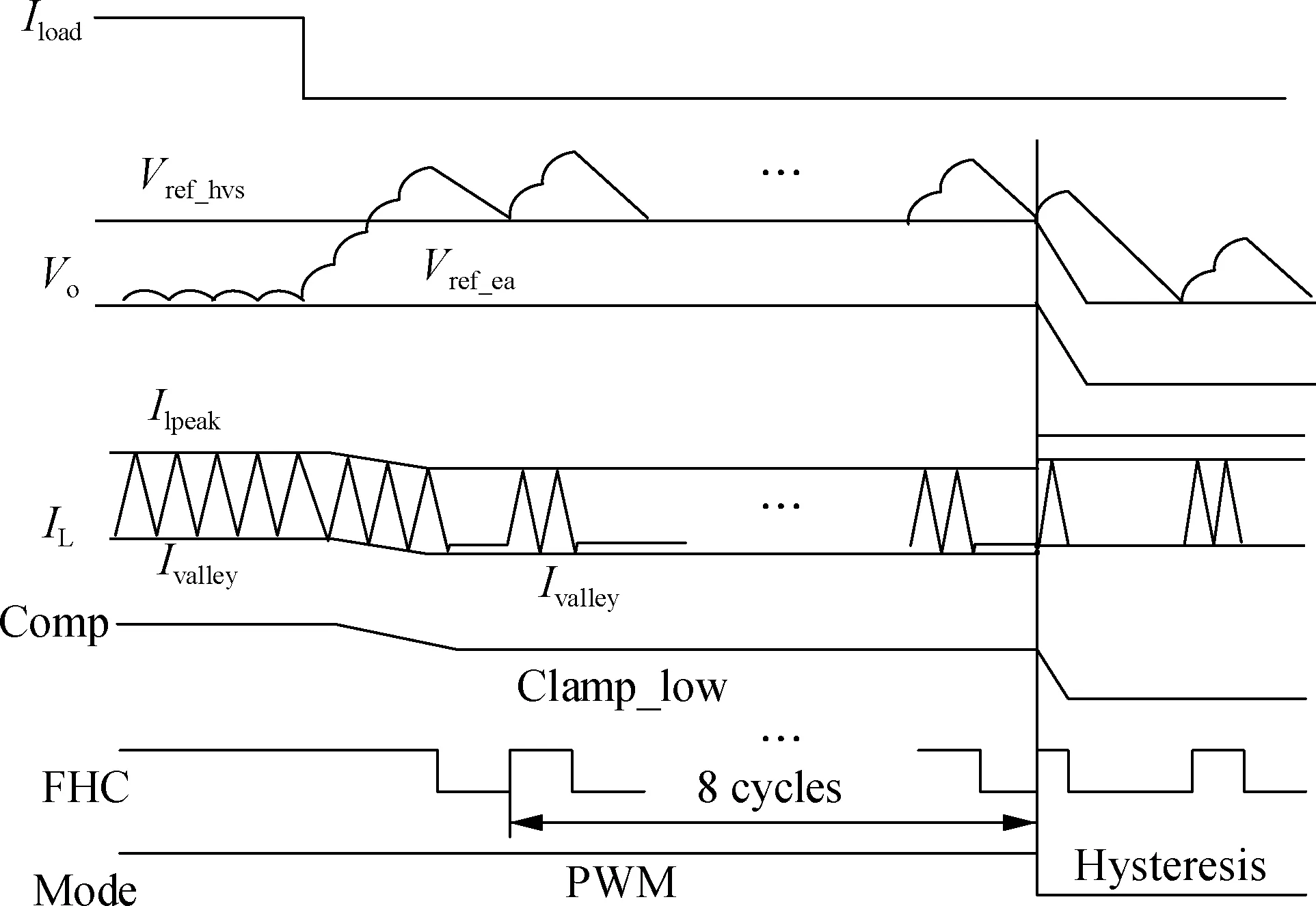
Fig.5 PWM to hysteresis mode transition of CICC
Under the hysteresis mode, the hysteresis frequency is defined by the hysteresis windowVh, peak currentIp, input voltageVin, output voltageVoand loadR.
(3)
Under PWM mode, the switching frequency varies with peak currentIp, input voltageVin, output voltageVoand inductanceL.
(4)
2.3 Small signal model
As the switching frequency in PWM mode varies with load current, introducetonandtsto replace dutydas the small signal variants,
(5)
Solve it with small signal perturbation,
(6)
Take buck mode as an example to deduce the small signal model,
ton=dts
(7)
(8)
(9)

(10)

(11)
(12)

(13)
According to the average model of the three-terminal device, the buck mode parameters of the CICC buck-boost can be defined as
(14)
(15)
(16)
The CICC buck mode small signal switch model is shown as Fig.6. HereKi=1 indicates it is the average inductor current control because peak current mode has the sample and hold delay in high frequency range that iski=He(s)=1-s/(1/Ts)+s2/(π/Ts)2. Therefore, the CICC mode is similar to the average current mode, but with better inner current loop response than peak current mode. The control-to-output transfer function is
(17)
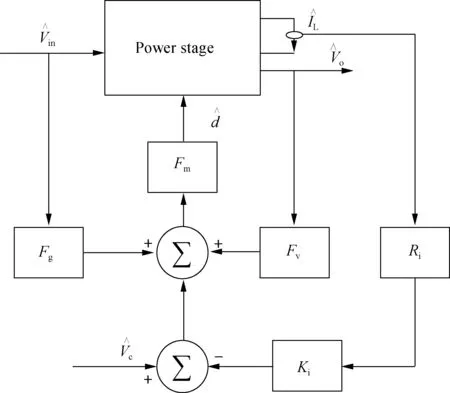
Fig.6 Small signal model diagram of CICC buck mode
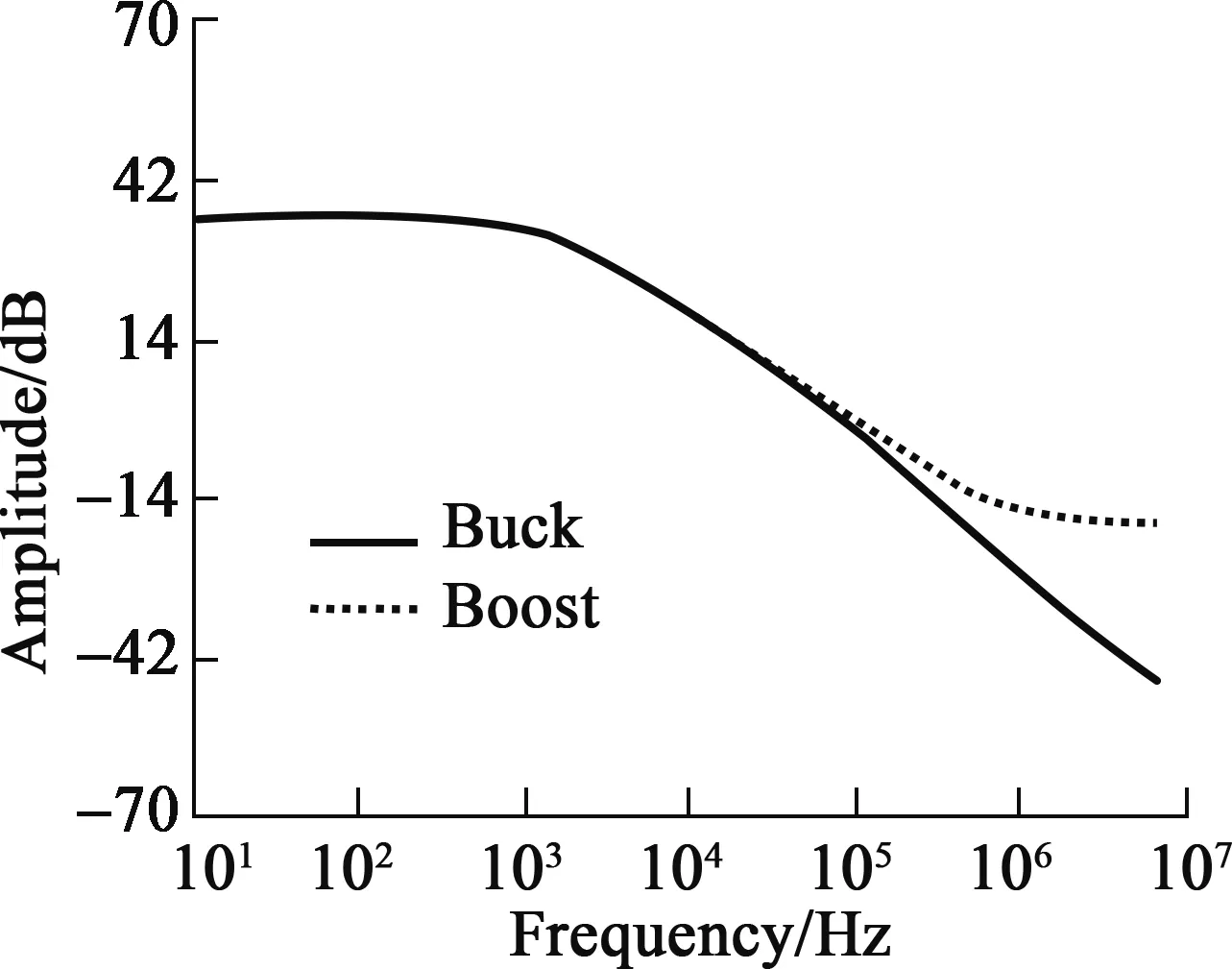
The loop modeling parameters of three operation modes are summarized in Tab.2. It is easy to extend to control-to-output transfer function of the boost and buck-boost mode. Fig.7 shows the control-to-output transfer function of buck and boost modes. These are both single pole systems so the converter keeps stable during the buck and boost mode transition.
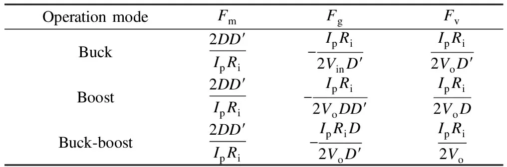
Tab.2 Loop modeling parameter summary
3 Experimental Results
Wide output voltage range (6-36 V) and input voltage (5-40 V) are achieved with 10 A maximum load current (2.4 A). The prototype specifications are listed in Tab.3. The typical output voltage is 12 V with 2.4 A peak to valleyIL. With ICSC control, the converter is operating in buck mode with 36 VVin, in boost mode with 6 VVinand in buck-boost mode with 12Vin. When the voltage difference is small betweenVinandVo, switch M1 and
(a)
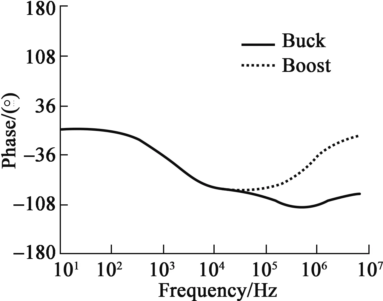
(b)Fig.7 Control-to-output transfer function of CICC buck-boost converter. (a) Amplitude; (b) Phase
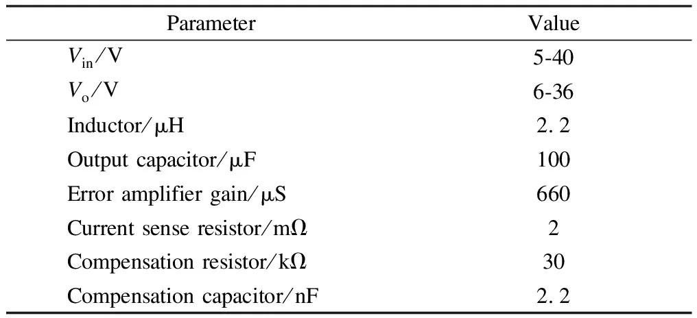
Tab.3 Prototype specifications
switch M4 are almost always on during the switching phase untilVois charged to larger than the reference rising threshold of the hysteresis comparator.
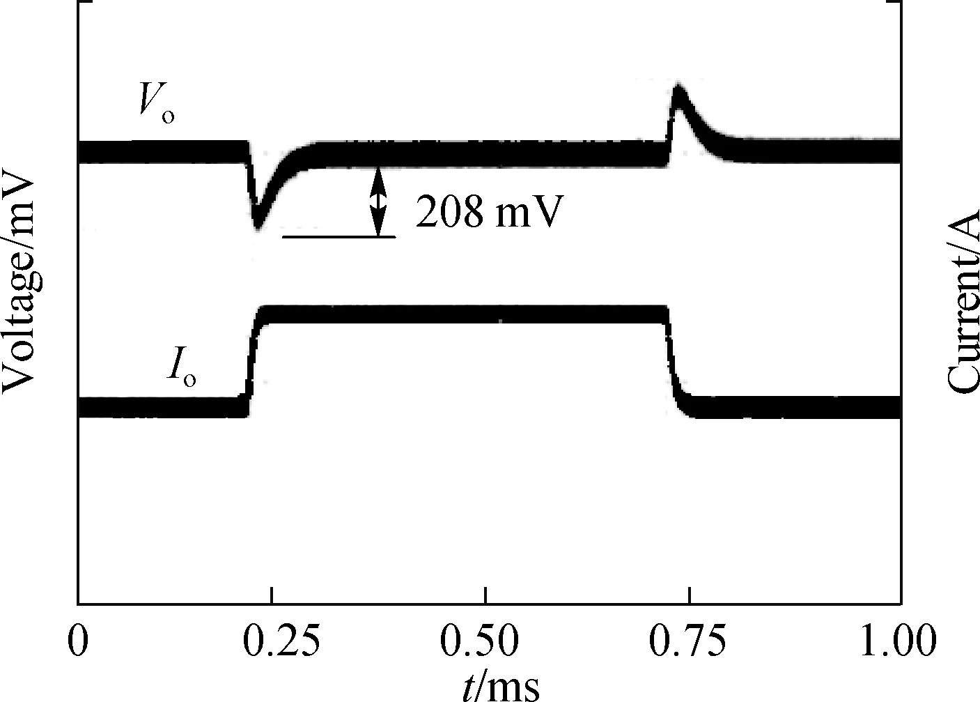
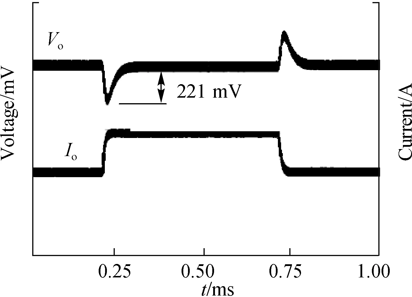
The load transient response is shown in Fig.8. The load step is 5 A, the half of the full load with 1 A/μs slew rate. The output voltage deviations are all less than 4%. Fig.9 is the line transient response. The maximum output voltage deviation is 3.8% with 7 to 18 V line transient and 0.1 V/μs slew rate.
Fig.10 illustrates the conversion efficiency in differentVin. The peak efficiency reaches 95% and the full load efficiency is 94%. Furthermore, the efficiency is greater than 76% when the load current is more than above 10 mA.
4 Conclusion
1) A novel ICSC non-inverting buck-boost converter with automatic and fast buck and boost mode transition in one switching cycle is proposed in this paper. The converter avoids the output voltage fluctuation with small output ripple.
(a)
(b)
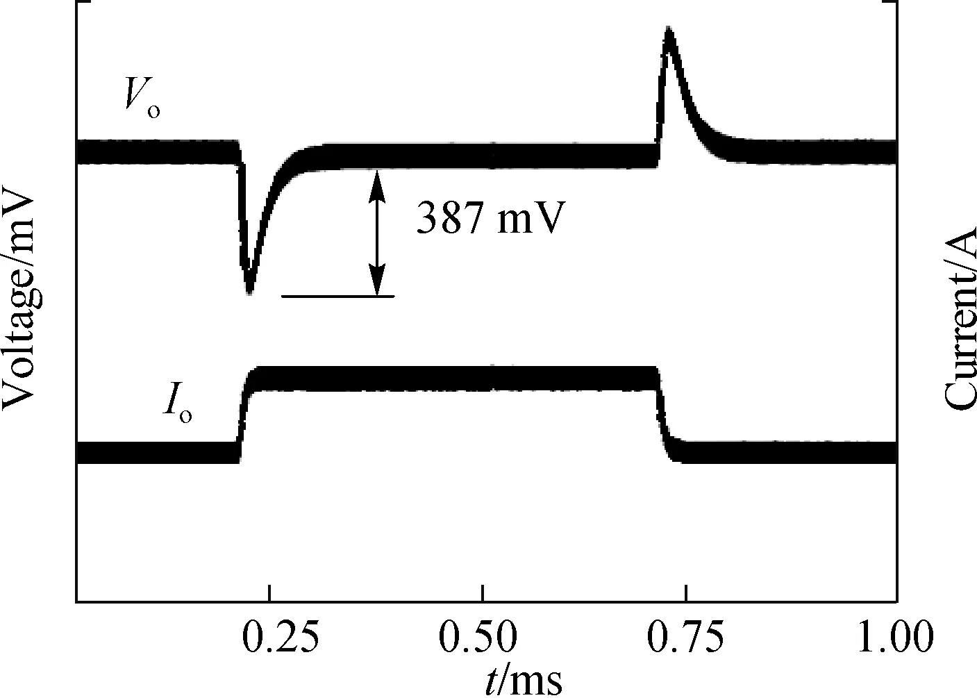
(c)Fig.8 Measured load transient performance. (a) Vin=36 V; (b) Vin=12 V; (c) Vin =6 V
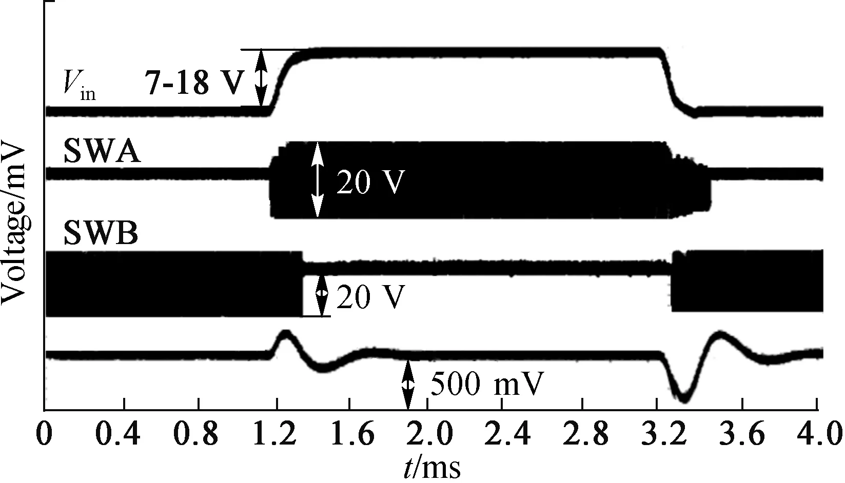
Fig.9 Measured line transient performance
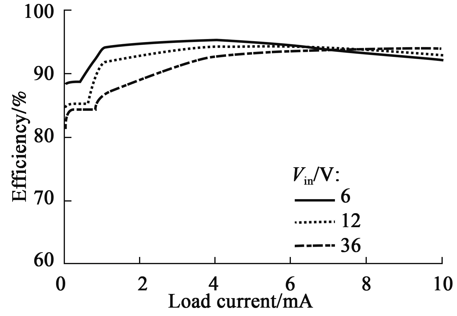
Fig.10 Measured efficiency
2) With the CICC control, the converter can also smoothly transit between hysteresis loop and PWM loop. The stability is verified with small signal analysis.
3) The load transient response measurement shows less than 4% deviation with half of full load step. It achieves the 95% peak efficiency and 94% efficiency at full 10 A load.
杂志排行

Journal of Southeast University(English Edition)的其它文章
- Effects of crankpin bearing speed and dimension on engine power
- A method for workpiece surface small-defect detection based on CutMix and YOLOv3
- Three-dimensional visualization interactive system for digital twin workshop
- Design and evaluation of cab seat suspension system based on negative stiffness structure
- Transformer-like model with linear attention for speech emotion recognition
- No-reference blur assessment method based on gradient and saliency