Characteristic mode analysis of wideband high-gain and low-profile metasurface antenna∗
2021-06-26KunGao高坤XiangYuCao曹祥玉JunGao高军HuanHuanYang杨欢欢andJiangFengHan韩江枫
Kun Gao(高坤), Xiang-Yu Cao(曹祥玉), Jun Gao(高军), Huan-Huan Yang(杨欢欢), and Jiang-Feng Han(韩江枫)
Information and Navigation College of Air Force Engineering University,Xi’an 710077,China
Keywords: characteristic mode analysis,wideband,high gain,metasurface antenna
1. Introduction
Microstrip patch antennas have been widely used in wireless communication, satellite communication for their excellent performances of low profile, easy conformal, and easy processing. Electromagnetic metasurface (MTS) provides the solutions to the inherent shortcomings such as low gain and narrow band,and greatly expands the performances,such as nano imaging,[1]phase modulation,[2–5]polarization conversion,[6,7]high performance,[8]etc.However,traditional MTS has limitations in application, and good MTS needs to be designed based on rich experience. The equivalent circuit theory,[9–11]effective medium theory,[12]surface impedance extraction,[13,14]and other theories have been used to characterize the MTS. But these methods are not suitable for MTS antenna analysis consisting of only a few units. The theory of characteristic mode (TCM) based on the method of moment (MOM) is a practical method of designing antenna,which can have an in-depth physical insight into the radiation phenomenon in the antenna. The TCM guides the design of MTS,and realizes the function of suppressing higherorder modes and exciting the desired modes to improve the radiation performance.[15]Recently, the TCM is used to analyze and optimize low-profile wideband metasurface antennas with microstrip feeding and coaxial feeding respectively.[16,17]In Ref. [18], the TCM is also used to analyze the orthogonal modal current with equal modal significance(MS)amplitude and phase difference of 90◦to find the optimal feeding point position and realize circular polarization. In Ref.[19], a new combined characteristic mode (CM) associated with low resistance resonances of slot antenna is introduced to increase the bandwidth of ring slot antenna by loading stubs. In addition,according to the guidelines of modal weighting coefficient(MWC),a low RCS T-shaped slot antenna is designed to suppress the scattering mode while maintaining the radiation mode by loading reactance components and slots.[20]So far,a small amount of work has been done on the design of high gain antenna in wideband range based on characteristic mode analysis(CMA).
In this paper,a metasurface antenna is designed for wideband high-gain and low-profile operation based on the CMA.The antenna is comprised of a rectangle patch fed by coaxial probe sandwiched between the metasurface composed of three sizes and the ground plane. The CMs of the proposed and original metasurface are in depth analyzed in order to explain the working principle and study the underlying modal behaviors of the metasurface and guide the mode excitation.The designed metasurface antenna length is 0.065λ0(λ0is the working wavelength of 6.5 GHz in free space). The designed antenna is in good agreement between simulation and measurement.
The rest of this paper is structured as follows. In Section 2, the characteristic mode theory of multilayered dielectric antenna is briefly introduced. In Section 3, the antenna structure is illustrated,the characteristic mode analysis of the proposed and original antenna are conducted,and the gain enhancement is analyzed. Section 4 reports the simulation of the antenna and the measurement environment. The final conclusions are given in Section 5.
2. TCM of multilayered medium
The theory of characteristic modes (TCM) was first introduced in 1965,[21]and in the few years that follows, it was further developed to analyze the radiation and scattering properties of dielectric and magnetic material bodies by the MOM.[22–25]The elements of the impedance matrixZcan be expressed by applying the standard Galerkin’s procedure to the MPIE.[26,27]Following the procedure of the conventional TCM for PEC bodies, a generalized eigenvalue equation for the MPIE can be written as

whereRandXare the real part and imaginary part of the impedance matrixZ,respectively.λnis the real eigenvalue associated with each characteristic currentJn,andndenotes the index of the order of each mode. Characteristic modes form a complete set of solutions,and hence the total current can be expressed as a linear superposition of these mode currents
whereαndenotes the modal weighting coefficient(MWC)and can be calculated from
where the termVinis called the modal excitation coefficient(MEC),andEiis the external excitation. The MS is expressed as

The mode resonates and radiates most efficiently when MS=1, that is,λn= 0. Suppressing unwanted modes requires reducing|αn|,or changing the unwanted modal current behaviors.
3. CMA of metasurface antenna
3.1. Antenna structure and design
The structure of the proposed antenna is shown in Fig.1.The antenna consists of three metallic layers,a metasurface,a microstrip patch, and a ground from top to bottom. The two F4B substrates (εr=2.65 and tanδ=0.0007) are both 1.5 mm in thickness. The metasurface is composed of three sizes of patches. It should be noted that the widths of the two patches adjacent to the center patch in thexdirection are bothSpand the two ends of the patche in theydirection are square patches,with each side beingWp.

Fig. 1. Structure of proposed antenna, with Wg =50 mm, Lg =50 mm,Wp=7.2 mm,Lp=8.9 mm,Sp=3.6 mm,Ws=0.65 mm,PW =7.2 mm,PL=12.3 mm,Lf=5.2 mm,ha=1.5 mm,and hf=1.5 mm.
3.2. CMA of proposed antenna structure
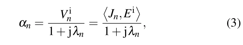
The CMs are obtained using the MoM-based CMA tool in commercial simulation software CST Studio Suite 2020,in which the ground plane and dielectric layers extend infinitely by using a multilayer solver. The dielectric loss is neglected in the CMA but considered in the time domain analysis, and all other geometric dimensions of the antenna are kept unchanged.

Fig.2. (a)Modal significance and(b)|MWC|versus frequency for several modes of antenna structure.
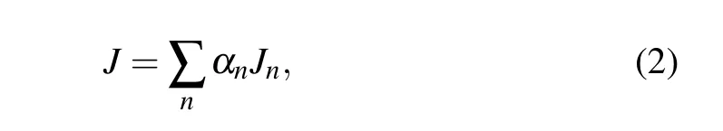
The calculated MS of the first eight modes of the proposed structure without the feed are plotted in Fig.2(a).Modal currents and radiation patterns ofJ1–J8are shown in Figs. 3 and 4,respectively. As can be seen,J1andJ7are linearly polarized along theyaxis with broadside radiation, whileJ3is linearly polarized along thexaxis.J2,J4,andJ5are symmetrical, and the patterns are split.J6is in the shape of a ring,which does not radiate outwards , and the main lobe of the mode pattern is concave. TheJ8is reversed in thexdirection and symmetrical in theydirection, and the side lobe level is higher. It can be seen thatJ1andJ7are the modes that need to be excited, and the other modes are unwanted modes. The mode electric field on the microstrip patch is shown in Fig.5.The feed point is marked with an empty circle. The coaxial feed is selected at the point where the modalE-field of theJ1andJ7are largest and the undesired mode excitation intensity is minimum. The coaxial probe fed by electric field coupling can be regarded as a capacitive coupling element(CCE).[28,29]If the CCE is placed at the peak of theJ1andJ7, the desired modes will be greatly excited. The modal weighting coefficients (MWCs) of the first eight modes are obtained from Eq.(3)to measure the ratio of each mode’s radiation power to the total radiation power as shown in Fig. 2(b). The excited mode current distribution is basically the same as that of the mode current without feed structure in Fig. 3. It can be seen thatJ1is dominant andJ7is partially excited in the higher frequency band. Some unwanted modes are well suppressed due to the selection of appropriate feeding position. In addition,J2andJ8are negligible compared withJ1andJ7.

Fig.3. Modal current distribution,for(a)J1 at 6 GHz,(b)J2 at 8 GHz,(c)J3 at 8 GHz,(d)J4 at 8 GHz,(e)J5 at 8 GHz,(f)J6 at 8 GHz,(g)J7 at 8 GHz,and(h)J8 at 8 GHz.
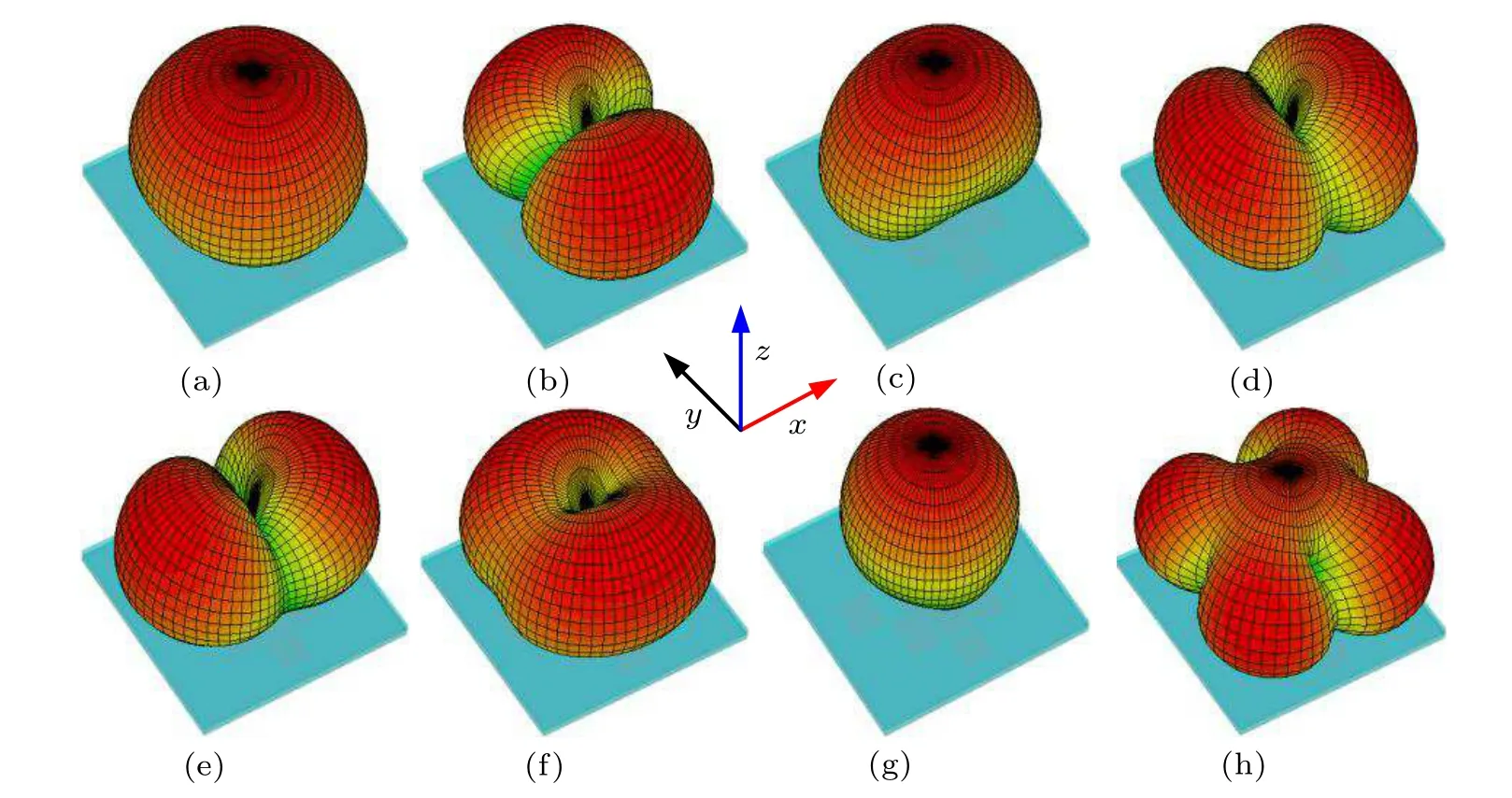
Fig.4. Modal radiation patterns for(a)J1 at 6 GHz,(b)J2 at 8 GHz,(c)J3 at 8 GHz,(d)J4 at 8 GHz,(e)J5 at 8 GHz,(f)J6 at 8 GHz,(g)J7 at 8 GHz,and(h)J8 at 8 GHz.

Fig.5. Modal radiation patterns,for(a)J1 at 6 GHz,(b)J2 at 8 GHz,(c)J3 at 8 GHz,(d)J4 at 8 GHz,(e)J5 at 8 GHz,(f)J6 at 8 GHz,(g)J7 at 8 GHz,and(h)J8 at 8 GHz.
3.3. Gain enhancement analysis
The top view of the original antenna structure is shown in Fig. 6(a), and the geometric dimension is kept unchanged exceptSpthat is changed into 7.2 mm. The CMA is performed on the original antenna with the coaxial feed structure,and the mode with coaxial feed excitation is more consistent with the actual excitation mode for the origin antenna structure. The mode current is shown in Fig.7,and MWC is shown in Fig. 6(b). TheJs1is dominant, whileJs5andJs7are also excited to different degrees at high frequency. TheJs5is symmetrical,andJs7is opposite to the current in theydirection of the center,which results in the large side lobe and the concave gain of the original antenna at high frequency. Figure 8 shows the reflection coefficient and gainversusfrequency of the original antenna, as well as the pattern at 5.5 GHz, 6.5 GHz, and 7.5 GHz,separately. It can be seen that the pattern has a larger sidelobe and a concave gain at 7.5 GHz.
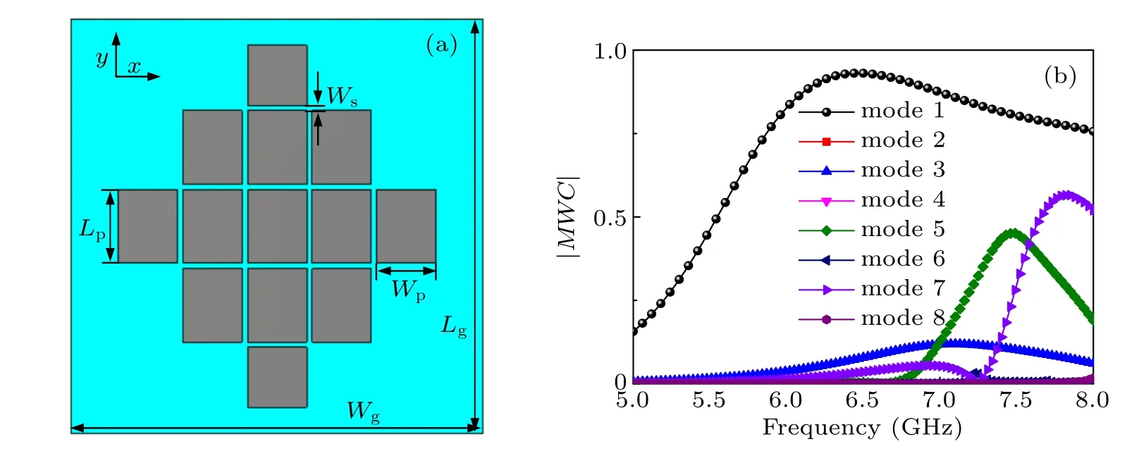
Fig.6. (a)Top view of original antenna structure and(b)|MWC|versus frequency for various modes of original antenna structure.

Fig.7. Modal currents distribution of original antenna for(a)Js1 at 6 GHz,(b)Js2 at 8 GHz,(c)Js3 at 8 GHz,(d)Js4 at 8 GHz,(e)Js5 at 8 GHz,(f)Js6 at 8 GHz,(g)Js7 at 8 GHz,and(h)Js8 at 8 GHz.
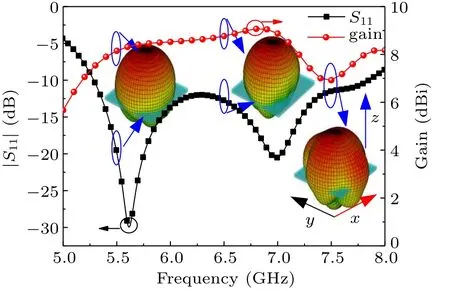
Fig.8. Reflection coefficient and gain versus frequency of original antenna,and pattern at 5.5 GHz,6.5 GHz,and 7.5 GHz.
In order to reduce the side lobe and enhance the gain,the patch named Spatch with widthSpin Fig. 1 plays a pivotal role in radiation performance,and the variations of impedance matching and gain with frequency for various values ofSpare studied as shown in Fig. 9. In the lower-end frequency band, the dominant mode currentJs1on the Spatch is in the identical direction with that on the center patch and the microstrip patch,and the boresight gain declines withSpdecreasing; in the upper-end frequency band, the higher-order mode current on the Spatch is different from that on the center patch and microstrip patch,and the boresight gain increases withSpdecreasing. Owing to the fact that the mode current on the Spatch cancels out the radiation,the gain drops sharply within 7 GHz–8 GHz, whenSpis 7.2 mm. WhenSpis greater than 3.6 mm,the−10-dB impedance bandwidth is satisfactory,andvice versa. The bandwidth is basically stable except for slight frequency shift. It is worth mentioning that the four corner patches and Spatch with 3.6 mm increase the antenna gain by 1.1 dB,and the two square patches expand the bandwidth. To summarize,Spis chosen to be 3.6 mm,which can improve the radiation performance.
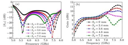
Fig.9. Effect of Sp on antenna,showing(a)|S11|and(b)gain versus frequency.
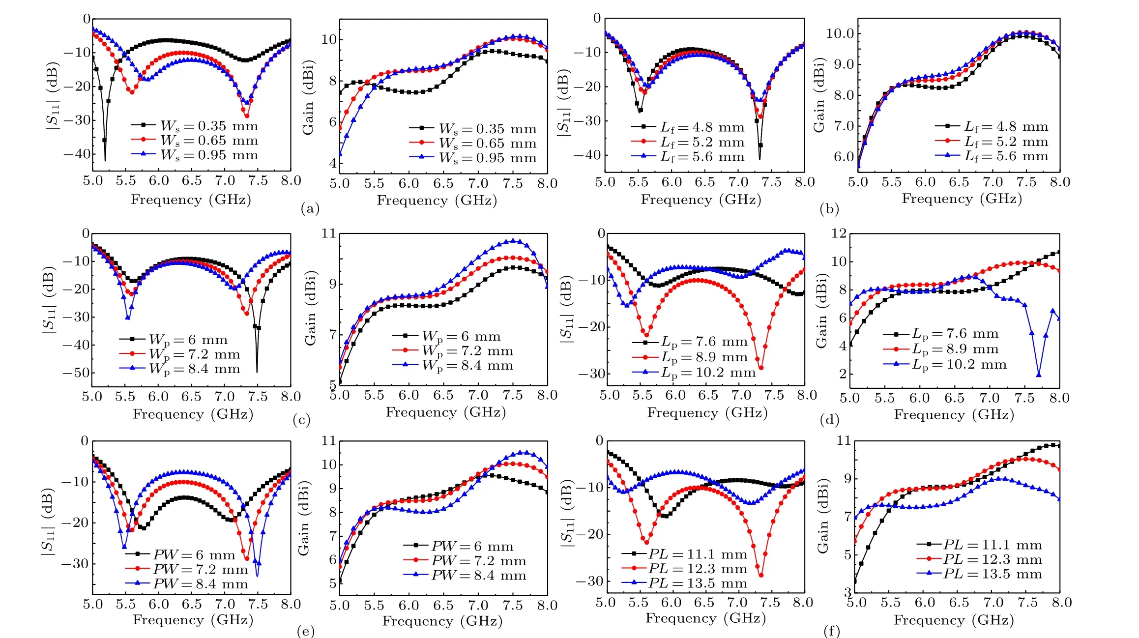
Fig.10. Effect of Ws,Lf,Wp,Lp,PW,PL on antenna|S11|and gain,(a)Ws,(b)Lf,(c)Wp,(d)Lp,(e)PW,(f)PL versus frequency.
3.4. Parameter study
With the increase ofPW, the impedance matching becomes worse, and the gain decreases at low frequency and increases at high frequency.LfandWphave little influence on the impedance bandwidth and gain, whileWs,Lp, andPLmainly contribute to impedance matching and gain.
4. Fabrication and measurement
The photograph of the proposed antenna and the anechoic chamber measurement environment are shown in Fig.11. By using the full-wave simulator,HFSS 14.0 simulator,the entire antenna is simulated and characterized to derive its radiation patterns. The simulated and measuredS-parameters and boresight gain are compared in Fig.12,and it can be seen that the simulated pattern sidelobe is reduced at 7.5 GHz. The discrepancy between the measurements and simulations may be attributed to the ungratified experimental measurement state,the accuracy of fabrication and the accuracy of mesh generation. The measured impedance bandwidth for|S11|=−10 dB is 39.8% (5.3 GHz–7.94 GHz), within which the boresight gain varies from 7.8 dBi to 10.04 dBi.
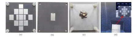
Fig. 11. Fabricated prototypes of proposed antenna, showing (a) top view, (b) middle patch view, (c) back view, (d) anechoic chamber measurement environment.
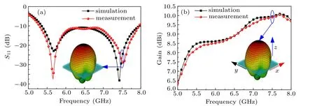
Fig.12. Simulated(Sim.) and measured(Mea.) results of(a)return loss and(b)gain.

Fig.13. Radiation patterns at(a)5.5 GHz for y–z plane,(b)5.5 GHz for x–z plane,(c)6.5 GHz for y–z plane,(d)6.5 GHz for x–z plane,(e)7.5 GHz for y–z plane,and(f)7.5 GHz for x–z plane.
Figure 13 shows the excellent agreement between the simulated and measured normalized radiation patterns at 5.5 GHz,6.5 GHz,and 7.5 GHz. Besides,the measured crosspolarization levels at boresight is below−30 dB across the operating band due to the suppression of undesired modes. The performance comparison between the proposed antenna and some other metasurface antennas based on CMA are shown in Table 1.

Table 1. Comparison of wideband patch antennas based on CMA between our proposed antenna and other reported antennas.
5. Conclusions
A wideband high-gain and low-profile patch antenna fed by coaxial probe using metasurface is proposed, analyzed,and experimentally verified. The wideband high-gain working mechanism is well explained and understood based on the CMA. Quantities and parameters of characteristic modes effectively guid the design, optimization, and excitation placement.
猜你喜欢
杂志排行

Chinese Physics B的其它文章
- Quantum computation and simulation with vibrational modes of trapped ions
- ℋ∞state estimation for Markov jump neural networks with transition probabilities subject to the persistent dwell-time switching rule∗
- Effect of symmetrical frequency chirp on pair production∗
- Entanglement properties of GHZ and W superposition state and its decayed states∗
- Lie transformation on shortcut to adiabaticity in parametric driving quantum systems∗
- Controlled quantum teleportation of an unknown single-qutrit state in noisy channels with memory∗