Organic Solar Cell Module Device Based on A Novel Composite Transport Layer
2021-03-05DINGLeiFOWanzhenDONGHaojie
DING Lei , FO Wan-zhen, DONG Hao-jie
(1. School of Electrical Information and Artificial Intelligence, Shaanxi University of Science and Technology, Xi’an 710021, China; 2. Jiangsu Jitri Org Optoelectronics Technology Co., Ltd., Suzhou 215215, China)*Corresponding Author, E-mail: dinglei@sust.edu.cn
Abstract: Based on a new composite interface transport layer, large-area organic solar cell module was fabricated by vacuum evaporation of organic small molecular materials. According to the transmittance spectrum, surface roughness morphology and surface wettability of transport layer, the surface roughness of active layers based on different substrates, the uniformity of blade coating and the influence of different transport layers on the performance of organic solar cells were analyzed. The experimental results show that when the electronic dense layer of 4,7-diphenyl-1,10-phenanthroline(BPhen) acetylimide is deposited on the surface of aluminum-doped zinc oxide substrate, the new composite transport layer is formed, which does not affect the light transmittance of the substrate in the range of 300-900 nm. In addition, the electron dense layer of BPhen can effectively improve the flatness and wettability of the substrate surface, which is beneficial to the subsequent scraping of the active layer solution and improves the quality and the stability of the coating film. By analyzing the surface roughness and three-dimensional morphology of the active layer film coated on different substrates, the surface roughness of the active layer film coated on the AZO(Al doped ZnO)/BPhen new composite transport layer was significantly reduced. It means that the new composite transport layer as substrate is beneficial to scrape out a uniform active layer film. As a result, the open circuit voltage(Voc), short-circuit current density(Jsc) and fill factor(FF) of rigid and flexible module device are significantly improved, and the power conversion efficiency(PCE) of the new rigid modular device is increased to 10.62%, which is about 13% higher than stand device. Importantly, the PCE of the flexible module device reaches 5.13%, which is also approximately 32% higher than AZO-based device.
Key words: new composite transport layer; organic solar cell module; electron dense layer
1 Introduction
Organic solar cells(OSCs) have attracted a wide attention due to their advantages of low cost, large area manufacturing, flexibility and environmental friendliness[1-6]. At present, organic solar cells are developing rapidly, in the laboratory stage their photoelectric conversion efficiency(PCE) has exceeded 17%[7-17]. Therefore, it is urgent to carry out relevant industrial studies, which is necessary for the preparation of high-efficiency organic solar cell module devices[18-23]. Therefore, organic solar cell modules prepared by doctor-blade coating(DBC) should have good repeatability and maintain excellent conversion efficiency. The film forming property, uniformity and stability of the active film will be affected by the surface morphology of the different transport layer substrate. In the process of large-area scraping and coating, the differences of film thickness in different areas, and bad surface morphology and blending state of active layer will lead to the attenuation of module device performance[24-28]. At the same time, an interface transport layer with excellent performance can greatly restrain intrinsic defects and interfacial defects, improve the efficiency of carrier collection, and improve the PCE of module devices, which has the potential to promote the industrialization of organic solar cells.
Thus, this research proposes a new type of composite transport layer based on AZO/BPhen small molecule materials, which was constructed by vacuum evaporation of BPhen on the surface of the blade coated AZO film. The method of combining blade coating and vacuum evaporation can realize the hole filling and defect passivation of AZO film, which can improve the carrier collection efficiency and the surface smoothness. Therefore, the stability and PCE of organic solar cell module were effectively improved. In addition, this method is suitable for the preparation of flexible organic solar cells with highly repeatability.
2 Materials and Methods
2.1 Materials
Indium tin oxide(ITO) glass was purchased from South China Xiang Science and Technology Company, Ltd.. AZO is Al doped ZnO[29]. Zincacetate dihydrate(Zn(CH3COO)2·2H2O, 98%) were purchased from Sigma-Aldrich. Aluminum nitrate(Al(NO3)3·9H2O, 99.99%) was purchased from Aladdin. BPhen was purchased from Shaanxi Lighte Optoelectronics Material. Chloroform(99.8%) was purchased from damas-beta. For the active layer, the mixture of Poly[(2,6-(4,8-bis(5-(2-ethylhexyl-3-fluoro)thiophen-2-yl)-benzo[1,2-b∶4,5-b′]dithiophene))-alt-(5,5-(1′,3′-di-2-thienyl-5′,7′-bis(2-ethylhexyl)benzo[1′,2′-c:4′,5′-c′]dithiophene-4,8-dione)](PM6)∶(2,2′-((2Z,2′Z)-(12,13-bis(2-ethylhexyl)-3,9-diundecyl-12,13-dihydro-[1,2,5]thiadiazolo[3,4-e] thieno [2″,3″∶4′,5′] thieno [2′,3′∶4,5] pyrrolo [3,2-g] thieno [2′,3′∶4,5] thieno [3,2-b]indole-2,10-diyl)bis(methanylylidene))bis(5,6-difluoro-3-oxo-2,3-dihydro-1H-indene-2,1-diylidene)) dimalononitrile)(Y6) at a weight ratio of 1∶1.2 with a concentration of 18 mg/mL was dissolved in Chloroform(CF).1-Chloronaphthalene(CN) was added to the CF at various concentrations of 1.5%.
2.2 Device Fabrication
As shown in Fig.1(a), it is a schematic diagram of the device structure of traditional OSCs. The structure of OSCs is ITO/AZO(20 nm)/PM6∶Y6(100 nm)/MoO3(10 nm)/Al(300 nm).
Fig.1(b) is a schematic diagram of the device structure of the new composite transport layer OSCs. The structure of OSCs is ITO/AZO(20 nm)/ 4,7-Diphenyl-1,10-phenanthroline(BPhen)(10 nm) PM6∶Y6(100 nm)/MoO3(10 nm)/Al(300 nm). Fig.1(c) shows the chemical structure of the material used in the device. The preparation process of the new composite transport layer OSCs device is as follows: (1)Glass substrate was polished first, and then an ITO film was plated on the glass by magnetron sputtering to form ITO conductive glass as the cathode of the solar cell. (2)Patterned laser etched ITO conductive glass. (3)AZO solution was scraped on the patterned ITO conductive glass(The slit height was 20 μm[23]. The substrate temperature was 40 ℃, and the scraping rate was 30 mm/s.). The film was obtained by annealing at 140 ℃ for 20 min in the air. (4)ITO coated with AZO film was placed in the nitrogen gloves box inside of the vacuum coating machine. When the cabin pressure was pumped to 3×10⁻⁴Pa, BPhen organic small molecular material of 10 nm was steam plated at a rate of 0.2 nm/s to construct the composite transport layer. (5)Take out the evaporated substrate and place it on the scraper in the air for scraping and painting the light absorption layer solution. The active layer solution is a binary system solution divided into two groups PM6 and Y6, with a ratio of PM6∶Y6=1∶1.2.(6)Stir all solutions for 6 h before used(The height of the slit is 20 μm, the substrate temperature is 60 ℃, and the scraping speed is 40 mm/s.). Then anneal at 110 ℃ for 10 min resulted in a light absorption film thickness of 100 nm. (7)The battery sheet scraped and coated with the light absorption film was placed in the vacuum evaporation machine. When the cabin pressure was pumped to 3×10⁻⁴Pa, 10 nm thickness of MoO3was evaporated as the cavity transport layer at 0.01 nm/s evaporation rate. (8)Take out the battery slice and put it into a mold for physical partition. 1 mm electrode is exposed for connecting the top and the bottom between modules to build the batteries connected in series. Then put the battery slice in the coating machine, evaporate the 300 nm aluminum electrodes at the evaporation rate of 0.1 nm/s after the cabin pressure is pumped to 3×10⁻⁴Pa.

Fig.1 (a)-(b)Schematic diagrams of the device structure of traditional OSCs and the new composite transport layer. (c)Chemical structure of the material used in the device.
Fig.2(a) and (c) show the design drawings of large-area OSCs, which comprising 12 cells connected in series. Each cell is 0.4 cm in width and 7.5 cm in length and the intervals is 0.1 cm. The total active area of a large-area OSC is 36 cm2. The output voltage could be controlled by dominant the amount of cells in series. The cathode of each cell is connected to the ITO of adjacent right-side cell for series connection. However, in the batteries connected in series, every cell must be good running to make sure the circuit is connected. Therefore, how to control the uniformity of film is important. Fig.2(c) and (d) show the metal mask used to define the active layer by mechanical scratch for the series connection amongst the cells. Fig.2(e) shows the blade coating process, which first uses a pipette to deposit solution and then spreads of solution through capillary action.

Fig.2 Design of large-scale patterned OPV in series with side view(a) and top view(c). (b)Photo of the knife’s edge. (d)A metal mask for active region definition and interconnection. (e)Blade coating process.
3 Results and Discussion
3.1 Physical Characteristics of Different Transport Layers
In order to study the influence of different transport layers on the performance of OSC devices, we prepared traditional transport layer AZO films and new composite transport layer AZO/BPhen films on glass substrates.Fig.3 shows the transmittance curves of the glass substrate/AZO and glass substrate/AZO/BPhen structures. It can be seen from the curve that when an electron dense layer is deposited on the AZO substrate surface, and it has no effect on the transmittance of the substrate in the range of 300-900 nm, which ensures that the overall performance of the module device was not be affected.

Fig.3 Transmittance curves of glass substrate/AZO and glass substrate/AZO/BPhen structures
Because the surface morphology of the transport layer substrate is different, the film forming property, uniformity and stability of the next layer of film prepared by scraping and coating will be further affected. So we prepared different transport layers with different morphologies for test.Fig.4 shows the roughness of the surface of the glass substrate/AZO and glass substrate/AZO/BPhen structure with two-dimensional view.

Fig.4 Two-dimensional plan view of surface roughness of glass substrate/AZO(a) and glass substrate/AZO/BPhen(b) structure
The arithmetic mean difference(Ra) of the active layer is reduced from 5.456 nm to 4.779 nm under different substrates(the glass substrate/AZO and glass substrate/AZO/BPhen structure).
From the figure we could recognize that when an electron dense layer(BPhen layer) is deposited on the electron transport layer(BPhen layer and AZO layer), the surface roughness effectively reduced, which is benefited to the increasing of stability and uniformity of subsequent active layer coating.
Fig.5 shows the three-dimensional surface morphologies of the glass substrate/AZO and glass substrate/AZO/BPhen structures. As shown in Fig.5, the glass substrate/AZO has a drastic fluctuation of the thickness, which indicates that the entire surface is not flat enough. By adding an electron dense layer, we can effectively fill the holes defects of the AZO substrate, which make the entire base surface more flat, and significantly impact the quality of the subsequent coating film.

Fig.5 Three-dimensional surface morphologies of glass substrate/AZO(a) and glass substrate/AZO/BPhen(b) structure
Then, we studied the difference of the surface wettability of different transport layers through measuring the contact angles. As shown in Fig.6, the contact angle(θ) of chloroform solution changed from 43.1° to 41.2° for the glass substrate/AZO and glass substrate/AZO/BPhen structure. It can be found that when the electronic dense layer of BPhen is added to the AZO surface, it can effectively improve the flatness and wettability of the substrate surface, which is also benefited to the subsequent knife coating process of the light absorption layer solution, thus improves the quality and stability of the coating film.

Fig.6 Contact angle test diagrams of glass substrate/AZO(a) and glass substrate/AZO/BPhen(b) structure
3.2 Characteristics of Active Layer Based on Different Transport Layer Substrates
An excellent interface transport layer can greatly reduce the intrinsic defects and interface defects, further improved the carrier collection efficiency and the photoelectric conversion efficiency of the module device. For this reason, we studied the surface roughness and morphologies of the active layer based on different transport layer substrates. As shown in Fig.7, when an electron dense layer is added to the electron transport layer, the surface roughness of the active layer scraped as a substrate has been significantly reduced. TheRaof the active layer is reduced from 6.452 nm to 5.887 nm for glass substrate/AZO and glass substrate/AZO/BPhen structure. This indicates that a flat base is beneficial to scraping a uniform surface film.
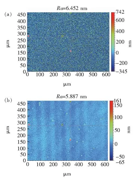
Fig.7 Two-dimensional plan view of the surface roughness of the active layer based on glass substrate/AZO/active layer(a) and glass substrate/AZO/BPhen/active layer(b) structure

Fig.8 Three-dimensional surface morphology of active layer based on glass substrate/AZO/active layer(a) and glass substrate/AZO/BPhen/active layer(b) structure

Fig.9 Film locations of different areas

Tab.1 Thickness of different areas of the active layer based on different substrates
3.3 Photovoltaic Characteristics of Organic Solar Cell Modules Based on Different Transport Layers
Based on two different transport layer substrates, we prepared the traditional organic solar cell module devices ITO/AZO/PM6∶Y6/MoO3/Al and new composite transport layer ITO/AZO/Bphen/PM6∶Y6/MoO3/Al organic solar cell module devices. Fig.10 shows the densityversusvoltage(J-V) curves of OSCs with BPhen of different thicknesses. The electron dense layer(BPhen) with 10 nm thicknesses is the most optimized device, which demonstrated a high photoelectric conversion efficiency(PCE) of 10.62%. The main effect of BPhen’s thickness is the electron transmission capacity for devices performance. If the BPhen’s thickness is too thick, the electron transmission capacity becomes weak. If it is too thin, which will not form an electron dense layer.

Fig.10 J-V curves of OSCs with BPhen of different thick-nesses
From theJ-Vand external quantum efficiency (EQE) curves of the rigid organic solar cell module devices with different structures as shown in Fig.11(a) and the photovoltaic parameters in Tab.2, we can found that when the composite transport layer is used, the uniformity of the morphology has a significant improvement. By improved and enhanced the carrier mobility, the device performance has been greatly improved, which mainly manifested by the increase in short-circuit current densityJscand fill factor FF,Jscincreased from 1.51 mA/cm2to 1.65 mA/cm2, FF from 63.04% to 64.15%. It shows that the film formed based on the new type of transport layer substrate has better film formation properties, fewer defects inside, and higher conversion efficiency of the absorbed photons. The PCE of the final prepared new rigid module device was improved to 10.62%, about an increase of 13%. As shown in Fig.11(b), the EQE of the device(from 450 to 800 nm) shows a slight improvement owing to the morphological optimization of blend films. Furthermore, 82% of EQE is obtained in the device with BPhen, exhibiting much stronger ability to collect carriers.

Fig.11 (a)J-V curves of rigid organic solar cell modules with different structures. (b)EQE curves of rigid organic solar cell modules with different structures.

Tab.2 Photovoltaic performance of rigid organic solar cell modules with different structures
Fig.12 shows the evolution of the PCE of cells under AM1.5(100 mW/cm2air mass 1.5 illumination). The performance of the reference cells degrades slowly. After 168 h, the PCE of the cells decreases from 10.62%(Voc=9.92 V,Jsc=1.65 mA/cm2, and FF=63.04%) to 9.26%(Voc=9.62 V,Jsc=1.50 mA/cm2, and FF=62.4%), and the PCE of traditional cell decreases from 9.40%(Voc=9.88 V,Jsc=1.51 mA/cm2, and FF=63.04%) to 5.23%(Voc=9.02 V,Jsc=1.08 mA/cm2, and FF=53.68%).Jscand FF of the large area devices are decreased, but new composite large-area modular devices show good stability.
From theJ-Vcurve of flexible organic solar cell module devices with different structures as shown in Fig.13 and the photovoltaic parameters in Tab.3, it can be seen that the new composite transport layer also has a good device performance on the flexible substrate. Compared with traditional module devices, the photovoltaic parameters have been greatly improved.Vocincreased from 8.59 V to 9.01 V,Jscincreased from 1.10 mA/cm2to 1.26 mA/ cm2and FF increased from 41.11% to 44.78%. In the end, the photoelectric conversion efficiency of its flexible module devices reached 5.13%, about an increase of 32%. Finally, it shows that adding an electronic dense layer on the surface of the rough PET substrate can effectively increase the surface flatness, which has great application potential in the improvement of the performance of flexible module devices in the future.

Fig.12 Evolution of the PCE of cells under AM1.5(100 mW/cm2 air mass 1.5 illumination)

Fig.13 J-V curves of flexible organic solar cell modules with different structures

Tab.3 Photovoltaic performance of flexible organic solar cell modules with different structures
4 Conclusion
In this study, a new type of composite transport layer is constructed by introducing an electron dense layer into the traditional transport layer. The combination of blade coating and evaporation techniques not only improved the optical and electrical properties of the film, but also reduced the roughness of the substrate and increased the substrate wettability. It is helpful for the film to form the active layer during the knife coating process, so that the film thickness is uniform and the morphology is structured. Finally, the overall photoelectric conversion efficiency of the rigid module device was greatly improved, and the PCE was increased from 9.4% to 10.62%. Moreover, it has a very good performance improvement effect on the flexible substrate, and the photoelectric conversion efficiency of the flexible module device has reached 5.13%, about an increase of 32% comparing to reference device. This research has a marked impact on the promotion of the industrialization of organic photovoltaic.
