Optoelectronic properties analysis of silicon light-emitting diode monolithically integrated in standard CMOS IC∗
2019-11-06YanxuChen陈彦旭DongliangXu许栋梁KaikaiXu徐开凯NingZhang张宁SiyangLiu刘斯扬JianmingZhao赵建明QianLuo罗谦LukasSnymanandJacobusSwart
Yanxu Chen(陈彦旭),Dongliang Xu(许栋梁),Kaikai Xu(徐开凯),†,Ning Zhang(张宁),Siyang Liu(刘斯扬),Jianming Zhao(赵建明),Qian Luo(罗谦),Lukas W.Snyman,and Jacobus W.Swart
1State Key Laboratory of Electronic Thin Films and Integrated Devices,University of Electronic Science and Technology of China,Chengdu 610054,China
2National ASIC System Engineering Research Center,Southeast University,Nanjing 210096,China
3Department of Electrical Engineering,University of South Africa,Pretoria 0001,South Africa
4Faculty of Electrical and Computer Engineering,State University of Campinas–UNICAMP,Campinas CEP 13083-852,Brazil
Keywords:silicon light-emitting diode,reverse bias,electro-optic modulation
1.Introduction
Silicon-based optoelectronic integration technology as the cornerstone of future information technology has great potential in optoelectronic applications.However,this technology faces a bottleneck of lacking suitable silicon-based light source due to the silicon’s indirect bandgap.To overcome this bottleneck,many silicon substrate light source schemes have been proposed.
In order to transform the indirect bandgap of silicon into direct bandgap,ultrathin SixGeystrained layer super-lattices were proposed to fold the Brillouin zone.[1]Although new optical properties in terms of Si-based optical devices were developed,it is difficult to obtain a relatively low epitaxial dislocation density. The lifetime of phosphorescent organic light-emitting diodes(OLED)is usually poor due to the trap formed by triplet-polaron annihilation.The exciton distribution can be broadened and the exciton concentration can be reduced by using ultrathin light emitting layers(<1 nm)and mixed bipolar interlayers.[2]The electro-optic performances and color stability can be further improved by changing the composition and the thickness of the buffer layer,which is in between the emitting and the electron transport layers.[3]Through adjusting the doping concentration of the quantum well barrier,a spectrum suitable for applications can be obtained. The effect of spectrum-control in dual-wavelength LED is due to the blocking effect of electrons and holes by doping quantum well barriers.[4]Nanocrystalline porous silicon receives much attention,in particular for its optoelectronic functions. Toward applications,there are two critical issues need to be highlighted:the luminescence quantum efficiency and its stability.[5,6]Erbium impurities are effective luminescence centers in silicon and exhibit sharp luminescence at 1.54µm.[7,8]However,the Er-doped device faces the limitation of emitting intensity. Si quantum dots embedded in SiOx/SiNx/SiCxmatrices are the key to overcome the shortcoming of poor emission efficiency in bulk Si.[9,10]Nevertheless,how to keep those embedded quantum dots stable is still a problem. In addition to Si based devices,deep-ultraviolet light emitting devices(DUVLEDs)also have a variety of potential applications.Zinc-oxide-based materials,which have wide bandgap and high exciton binding energy,have potential applications in high-performance DUVLEDs.To realize such optoelectronic devices,the modulation of the bandgap is required.[11]
Light emission from silicon devices has been realized in reverse-biased p–n avalanche structures.[12]High speed is required in optical interconnects,and GHz modulation bandwidth will limit the applications of this technology.[13]The purpose of this paper is to present our efforts on searching for the high speed of a silicon p–n junction switching of light emission.
In this study,the avalanche impact ionization process is presented to evaluate the emitted photons. The operational speed of avalanche breakdown mode is determined by the RC time constant of the device,as well as the carrier transit time through the depletion region.[12]Our study suggests that the device working under avalanche breakdown mode has a potential to reach gigabit rates.
2.Device fabrication
The proposed Si optoelectronic device structure is realized on a Si substrate by using typical silicon CMOS process technology.Starting from a 1-µm-thick n-typesilicon layer,an active region with p-type heavy doping is deposited on the surface through standard lithography and wet etching techniques.The device described in this paper has a width of 175.5µm and a length of 6µm,and the cross-sectional view is schematically given in Fig.1.
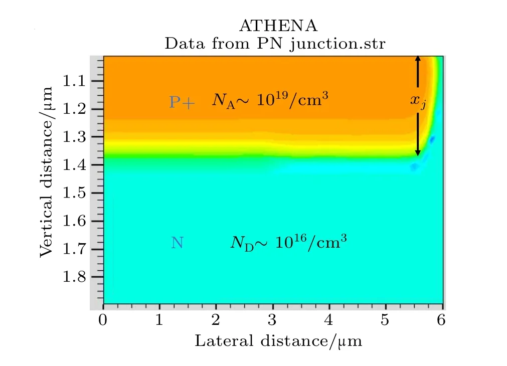
Fig.1.Cross-sectional view of the Si optoelectronic device structure.
3.Structural and optical properties of the device
As the reverse bias of the p–n junction increases,electrons and holes are accelerated to attain enough energy in the avalanching region with high electric field.When the reverse bias causes junction breakdown,newly generated electronhole pairs collide with the lattice and transfer energy to realize light emission.Indeed,both electrons and holes are excited in the related excitation zone in the avalanching junction.Hot electrons may recombine with hot holes in the excitation zone,[14]contributing to photons emitted from the high-field region in the avalanching p+n junction shown in Fig.2.
The avalanche breakdown voltage(BV)is numerically calculated using the background doping dependent model given as[15]
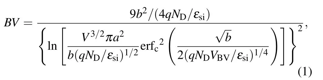
where a and b are constants related to the breakdown,q is the electron charge,and V is the voltage of reverse bias;NDis doping concentration of the substrate,and εsiis the dielectricity of silicon.Accordingly,the p–n junctions BV is ∼30 V for a 1016cm−3background doping concentration.
Tam and Hu measured the difference between the temperature dependence of the driving current and the temperature dependence of the photon-induced current.[16]The photon energy emitted from the reverse-biased p–n junction can be investigated by a dependence of hot-carrier effects on electron temperature.Accordingly,the photon energy intensity distribution function is given as
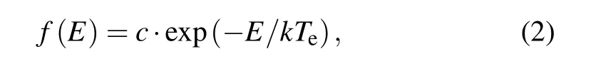
where c is a constant,k is the Boltzmann’s constant,E is the energy of photon,and Teis the effective temperature of the hot carrier.[17]
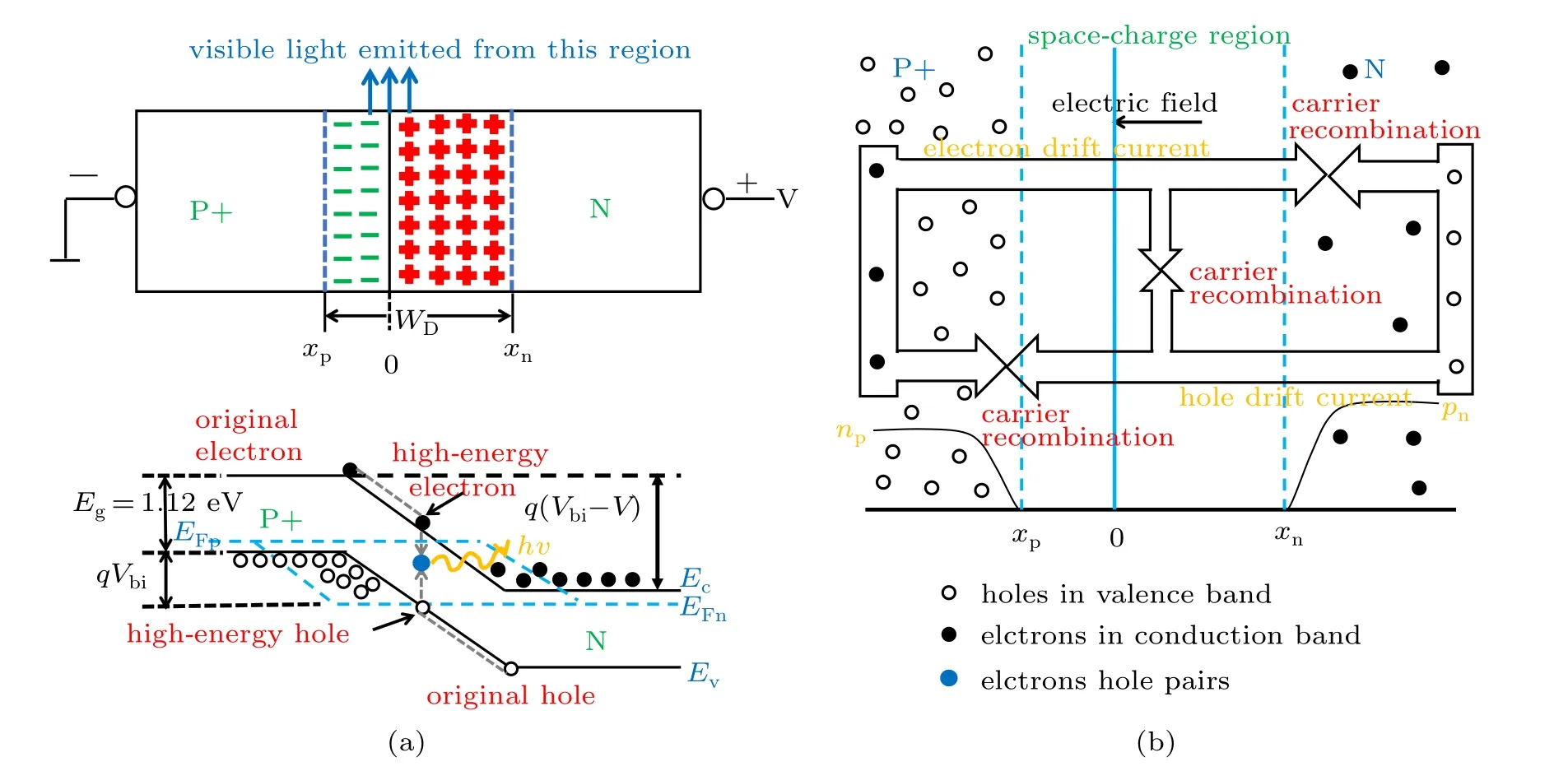
Fig.2.Schematic photon emission phenomena in Si avalanching junction.
As shown in Fig.3(a),when the reverse bias is over 30 V,the p–n junction starts to have avalanching breakdown,where the electric field peak surpasses 1.6×10⁵V/cm.The depletion width becomes wider slightly with the increase in the reverse biased voltage.Since the increase of the electric field is almost uniform,the relationship between the field’s maximum and the reverse bias voltage is very close to a linear dependence,as depicted in Fig.3(b).
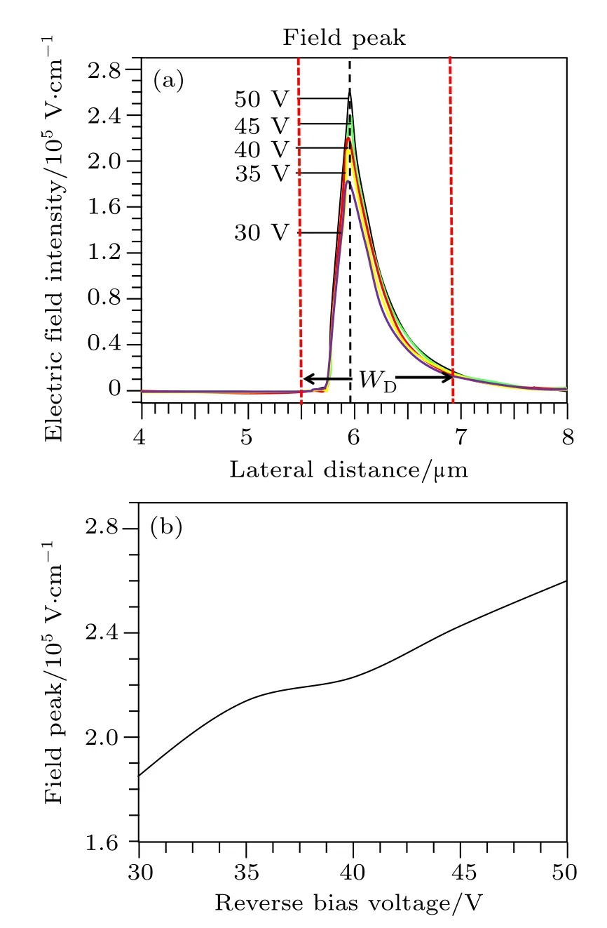
Fig.3.Characterization of the depletion region:(a)simulated electric field distribution in the drift region obtained through Poisson equation integration;(b)field peak as a function of reverse biased voltage.
The process of filament formation sets an upper limit to the light modulation speed. The filament formation time is typically governed by the transit time of the carriers reaching the depletion edge of the p–n junction.And it is given as

where WDis the depletion width and v is the saturated drift velocity of the electrons. For a breakdown voltage of 30 V,the depletion width of the junction under the reverse bias is approximately 1.4µm and the saturated drift velocity is 107cm/s,resulting in the theoretical limit of light modulation at ∼14 ps. For more luminous wider junctions having larger breakdown voltage,the time required for filament formation is longer(about a few hundred picoseconds),limiting the speed of light emission lower than 10 GHz.[18]In this case,the corresponding speed for the specific p–n junction diode is ft=1/(2πt)=11 GHz.
The capacitance in the structure of p–n junction diodes is another way to investigate the transient characteristics of the p–n junction structure-based silicon light source.The capacitance in the structure is defined in Fig.4,in which there is a capacitance associated with the depletion layer of the diode.As the diode is switched from off(zero-biased or reverse-biased)to on(forward-biased),it takes some time before the diode is turned on and reaches the steady state.This time is associated with charging up the depletion-layer capacitor and filling up the p-and n-regions with excess minority carriers.Similarly,when a diode is switched from the on state to the off state,it also takes some time before the diode is turned off. This time is associated with discharging the depletion-layer capacitors and discharging the excess minority carriers stored in the p-and n-regions.The majority-carrier response time,or the dielectric relaxation time,is much shorter,on the order of 10 ps.
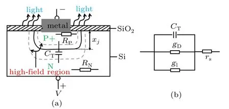
Fig.4. Capacitance in a p–n junction diode structure:(a)schematic view;(b)equivalent circuits of a p–n junction capacitor.
Time is needed to charge and discharge the depletionlayer capacitor.The depletion-layer capacitance CTas shown in Fig.4 is typically on the order of 1 fF/µm2.When the diode is operated,the current density J is of 1 mA/µm2.Then the time associated with charging and discharging the depletionlayer capacitor is of the order ofCTV/J,which is of the order of 10 ps.Of course,this time changes in proportion to the current density J.However,as we will show below,the time needed to charge or discharge the depletion-layer capacitor is usually very short compared with the time associated with charging or discharging the p-and n-regions of their majority carriers.In addition,in Fig.4,gDdenotes the p+n junction’s transconductance under DC condition,glis the intrinsic transconductance related to the junction’s leakage current,depending on the device fabrication process,and rsis the resistance(which is mainly consisted of the sheet resistance of the p-type and n-type layers in Fig.1).
Since the cross section’s area of the junction is W×L=175.5µm×6µm,the total capacitance C=CT×(WL)is of the order of 10−16F.The capacitance CTof the silicon p+n junction diode under the reverse-bias was simulated using the device simulator MEDICI[19]to understand the transient nature of electro-optic modulation.[20]As shown in Fig.5,the simulated depletion capacitance is plotted as a function of junction’s reverse bias voltage. The capacitance of the p–n junction based silicon light source decreases with the driving voltage when the device is turned on to avalanche breakdown.Stronger recombination in the luminescence active region induces negative capacitance phenomena.[21]
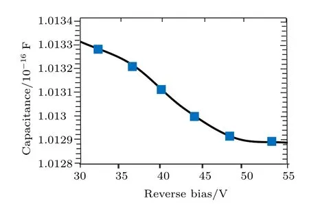
Fig.5.Parasitic capacitance–voltage characteristic of the silicon lightemitting device with p–n junction structure.
The forward-biased operation of p–n junctions for light emission is a slow,inefficient,and unreliable process because of the lifetime of the minority carriers. Any attempt to increase the speed of operation by removing the minority carriers reduces the efficiency of light emission.[18]The dynamic on-resistance of the p–n junction in avalanche is in the tens of kΩ range and the reverse-biased junction capacitance is in the range of pF.Then the RC time constant will be in the range of tens of ps.This will be sufficient to produce modulation in excess of 10 GHz.[22]Both the carrier lifetime depending on the electric field model and the capacitor’s discharging time depending on the RC time constant verify that a combined switching speed in the range of 10 GHz may still attainable for the p–n junction carrier injection light-emitting device in silicon devices.[12]
In avalanche mode,the electron–hole pairs can be accelerated by the electric field as well as gain excess energy.Those pairs could recombine radiatively.Figure 6 shows the silicon band structure model processes.The mechanisms of this recombination are as follows:hot electrons and holes recombine band-to-band,bremsstrahlung of the electrons corresponding to transitions within the conduction band and recombination of holes in the valence band.[20]As shown in Fig.7,spectroscopic measurements of the emitted light reveal clear emission peaks at 1.75 eV and 2.07 eV in the 400–900 nm wavelength region. In general,the mechanism of indirect interband transitions of energetic electrons in the conduction band and holes in the valence band is for low photon energy levels.Bremsstrahlung radiation is suggested for interpreting the intermediate photon energy level,and direct and indirect interband recombination contributions for high photon energy levels.The mechanisms of recombination could explain why those main radiation wavelength peaks are not close to the bandgap.
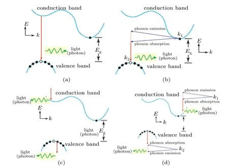
Fig.6.Possible photonic energy transitions in the silicon band diagram:(a)direct-interband transition,(b)indirect-interband transition,(c)direct-intraband transition,and(d)indirect-intraband transition.
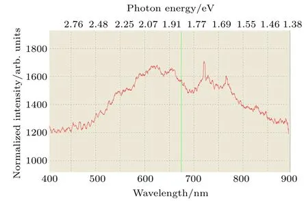
Fig.7.Intensity spectra of the p–n junction based silicon light-emitting device in the injection-avalanche mode of operation for various injection current levels(in this case a reverse current of 45 mA induced by the junction’s avalanching is applied).
We measured the emission power from the Si p+n junction device by using a calibrated power meter.The external quantum efficiency ηQ,which describes the conversion of carriers into photons,can be written as

Here,q is the elementary charge,λ is the wavelength,h is the Planck constant,c is the speed of light,and I is the reverse current.The power conversion efficiency ηPis defined as
where V is the reverse bias voltage,P is the externally measured optical output power,and I×V is the current–voltage product which means the applied total electrical power. By substituting Eq.(5)into Eq.(4),the relationship between the quantum efficiency and the power conversion efficiency can be derived as
The emission efficiency is presented in Fig.8.[23]

Fig.8. Efficiency of Si p+n junction. For instance,at the reverse bias V=40 V,the quantum efficiency(blue diamonds)is about 6×10⁻⁸ and the power conversion efficiency(pink squares)is 2.8×10⁻⁹.
Manufacturing these photonic devices is still a challenge.The processing starting with the same silicon wafers in microelectronics has been ubiquitous for decades.Optical components and circuitry onto wafers alongside the microelectronic elements have been introduced using many manufacturing tools in standard semiconductor fabs. However,because photons fundamentally do not obey the same physics as electrons,guiding a photon from one element to another inside a packaged chip is not as simple as soldering the two together. Thus alignment tolerances are much more exacting. Whereas connecting a wire to a contact-pad on a chip involves aligning the components to within a few tens of micrometres of the correct position,connecting an optical fibre to a photonic chip can require three orders of magnitude more precision.Fortunately,thanks to ingenious device engineering and some groundbreaking micro-robotic industrial automation technology,we are well on our way to overcoming these challenges,bringing high-throughput photonic interconnects into the mainstream.
4.Conclusion and perspectives
A transient model to establish a relationship of light emission from avalanche breakdown in Si p–n junctions with the applied reverse bias voltage is demonstrated.Theoretical simulations and experimental measurements of the capacitances and series resistances indicate that the device has an intrinsic high-frequency operating capability in the near gigahertz range. The spectral radiance as a function of wavelength is also shown,which reveals clear high intensity peaks at about 625 nm and 725 nm.A compatible CMOS technology lightemitting device is proposed with an optical output of several nW.Hence,some interesting chip-to-chip and on-chip electrooptical applications seem feasible in the next-generation VLSI integrated circuitry.
Acknowledgment
The authors thank Prof.Ian White of the University of Cambridge for useful suggestions.
杂志排行

Chinese Physics B的其它文章
- Compact finite difference schemes for the backward fractional Feynman–Kac equation with fractional substantial derivative*
- Exact solutions of a(2+1)-dimensional extended shallow water wave equation∗
- Lump-type solutions of a generalized Kadomtsev–Petviashvili equation in(3+1)-dimensions∗
- Time evolution of angular momentum coherent state derived by virtue of entangled state representation and a new binomial theorem∗
- Boundary states for entanglement robustness under dephasing and bit flip channels*
- Manipulating transition of a two-component Bose–Einstein condensate with a weak δ-shaped laser∗