Study on the nitridation of β-Ga2O3 films∗
2019-08-16FeiCheng程菲YueWenLi李悦文HongZhao赵红XiangQianXiu修向前ZhiTaiJia贾志泰DuoLiu刘铎XueMeiHua华雪梅ZiLiXie谢自力TaoTao陶涛PengChen陈鹏BinLiu刘斌RongZhang张荣andYouDouZheng郑有炓
Fei Cheng(程菲), Yue-Wen Li(李悦文), Hong Zhao(赵红),†, Xiang-Qian Xiu(修向前),,‡,Zhi-Tai Jia(贾志泰), Duo Liu(刘铎), Xue-Mei Hua(华雪梅), Zi-Li Xie(谢自力), Tao Tao(陶涛),Peng Chen(陈鹏), Bin Liu(刘斌), Rong Zhang(张荣),§, and You-Dou Zheng(郑有炓)
1Key Laboratory of Advanced Photonic and Electronic Materials,School of Electronic Science and Engineering,Nanjing University,Nanjing 210093,China
2State Key Laboratory of Crystal Materials,Shandong University,Jinan 250100,China
Keywords: β-Ga2O3,nitridation,GaN,single-crystal
1. Introduction
GaN-based nitrides have been widely used in optical devices and high power or high temperature microelectronic devices.[1-3]However,one of the main problems for high quality GaN growth is lack of a suitable lattice-match substrate.Foreign substrates,such as sapphire and Si,bring about a large number of defects in GaN epilayers,although they are the most popular substrates.[4,5]The ideal substrate would be GaN for the homoepitaxy.
β-Ga2O3is an ultra-wide band gap semiconductor and has excellent properties, such as high transparency in the region from visible to UV regions, high electrical conductivity and thermal stability at high temperature.[6-8]The lattice mismatch between GaN and β-Ga2O3is relatively small, as low as 2.6%.[9]So, β-Ga2O3can also be applied as a substrate for GaN epitaxial growth.[10,11]It has been reported that the(100) cleavage plane of β-Ga2O3undergoes a surface reconstruction under nitridation at high temperature and NH3gas,which causes the surface to match GaN naturally.[12]The surface of β-Ga2O3film can be nitridated to acquire good latticematching of GaN for the direct growth of GaN. And, GaN films converted from β-Ga2O3by nitridation with NH3can be also used as a substrate or template for GaN homogeneous epitaxial growth.In this work,we report the influences of temperature and time on the nitridation to better understand the process.
2. Experimental details
The 2-inch (1 inch=2.54 cm) β-Ga2O3films have been grown by self-made halide vapor phase epitaxy (HVPE)system.[13]The as-grown β-Ga2O3is transparent and smooth,the surface roughness is about 6.2 nm obtained by the analysis of atomic force microscope. The as-grown β-Ga2O3films have been cut into 1 cm×1 cm for the nitridation process. The nitridation of β-Ga2O3films has been carried out in a quartz tube furnace with the NH3flow rate of 200 sccm at different temperatures and times, respectively. After nitridation, all the samples exhibit yellowish and translucent.The surface morphologies were studied by scanning electron microscopy (SEM, JSM-700 F). The structural properties were measured by means of high-resolution x-ray diffraction(XRD,BRUKER-D8)and Raman spectroscopy(Raman,OLYMPUS-BX41).
3. Results and discussion
3.1. Analysis of nitridation temperature
Figure 1 shows the surface morphologies of β-Ga2O3film and as-nitridated films at different temperatures for 0.5 h.The scanning electron microscopy images randomly observed at different areas indicate that the surface morphology of asnitridated film is similar and uniform.It can be seen that lots of holes appear in the surface after nitridation.In the higher mag-nification,the surface consists of lots of hillock pits,showing a stratified or sheet structure. The rough surface may be due to the nitridation of β-Ga2O3at NH3atmosphere,and the β-Ga2O3decomposed into GaO, Ga2O, and Ga, releasing O2simultaneously.[14]More tiny hillock pits appear obviously in the surface of sample with increasing the temperature. When the nitridation temperature is up to 1000°C and above,the β-Ga2O3film is nitridated heavily and show a porous network structure. The decomposition and nitridation of β-Ga2O3at high temperature may results in the porous layer.[15]The density and diameter of the hillock pits increased as the nitridation temperature was increased from a temperature range of 850°C-1050°C due to the enhancement of the β-Ga2O3decomposition rate.[16]
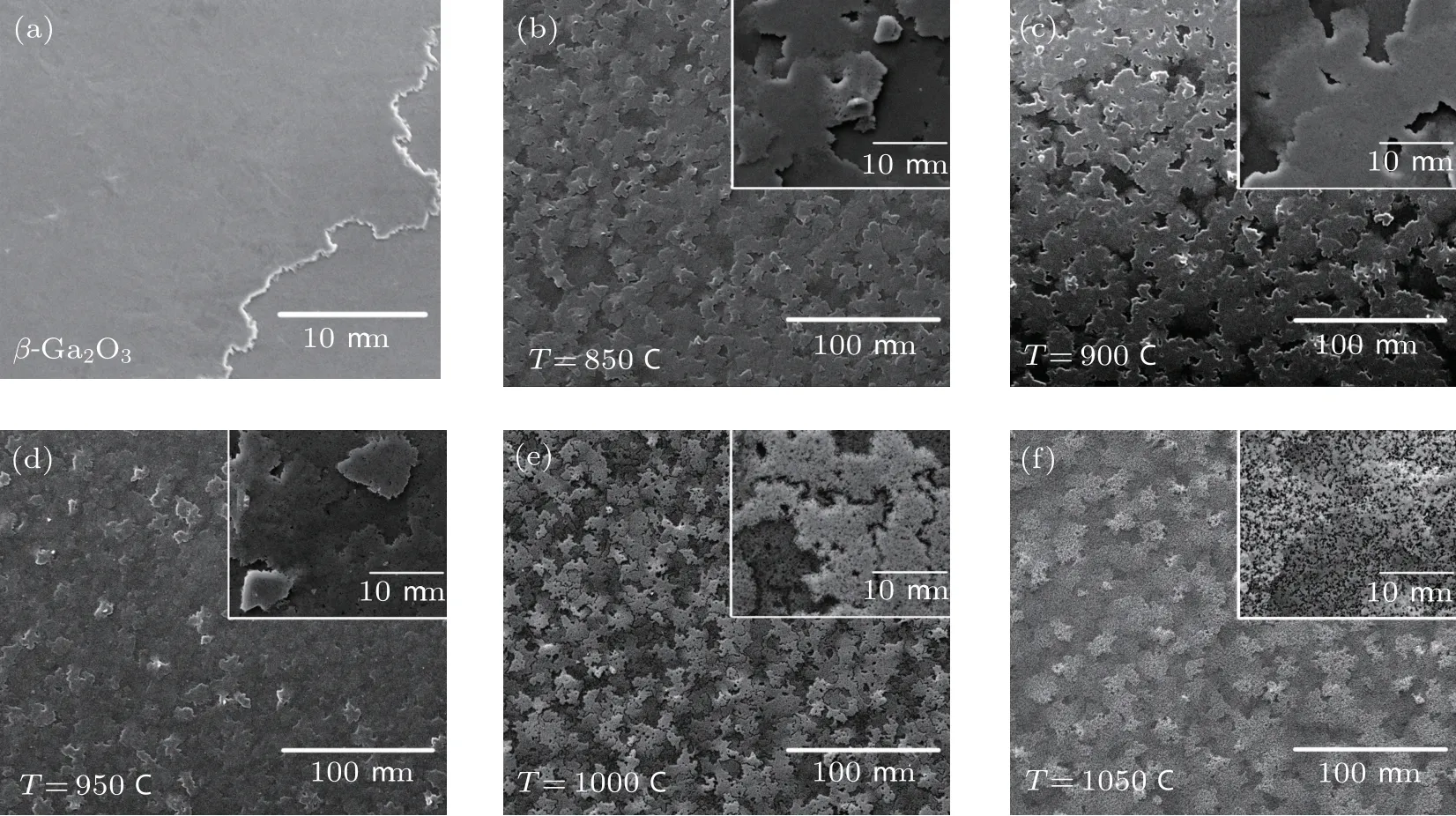
Fig.1. The SEM images of β-Ga2O3 film and the samples after nitridation at different temperatures for 0.5 h. The insets are SEM images in the higher magnification.
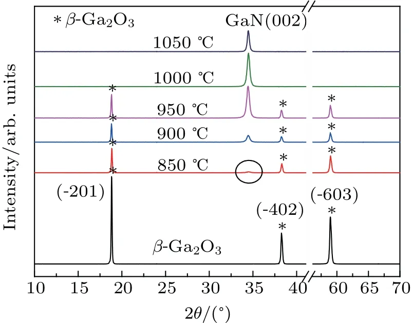
Fig.2. XRD patterns of β-Ga2O3 film and the samples after nitridation at different temperatures for 0.5 h.
The XRD patterns(θ-2θ scan)of β-Ga2O3film and asnitridated films at different temperatures for 0.5 h are exhibited in Fig.2. The XRD peaks at 18.84°,38.3°,58.98°correspond to diffractions from the(-201),(-402),(-603)planes of β-Ga2O3, respectively.[17]When the nitridation temperature is 850°C, the peaks of β-Ga2O3are dominant and a weak peak for the GaN (002) reflection occurs at 34.4°.[18]It indicates that β-Ga2O3have been converted partly to GaN at 850°C. The intensity of GaN (002) diffraction peak gradually increases and the full width at half maximum (FWHM)decreases with the increasing nitridation temperature. Conversely,the intensity of peaks belonging to β-Ga2O3gradually decreases. After a further increase of the nitridation temperature to 1000°C, the diffraction peaks belonging to β-Ga2O3entirely disappear and only a high intense single sharp XRD peak corresponding to GaN(002) plane dominates. XRD results reveal that the crystalline quality of the formed GaN increases with increasing nitridation temperature and the GaN films have a preferential orientation along(002)direction.
Raman spectra has been measured at room temperature by using an argon ion laser (λ =514 nm). Figure 3(a) illustrates the Raman spectra of β-Ga2O3film and as-nitridated films at different temperatures for 0.5 h. For β-Ga2O3, eight Raman peaks were observed with no blue shift as compared to the bulk Raman peaks.[19]After nitridation at 850°C, the Raman spectra shows no obvious changes,expect a slight reduction of the peak intensity. For β-Ga2O3films nitridated at 950°C and 1000°C, the phonon modes related to β-Ga2O3are diminished and the Raman peaks corresponding to GaN at 142 cm-1,422 cm-1,568.8 cm-1,and 734 cm-1evolved.The Raman peak at 568.8 cm-1for the E2(high) phonon mode of GaN shows a slight blue-shift as compared to the standard Raman spectra of bulk GaN crystal,[20-22]which may results from lattice strain by the conversion from β-Ga2O3to GaN. During the nitridation process, the N atoms decompos-ing from NH3would replace the O atoms in Ga-O6or Ga-O4bond configurations to form Ga-N4or Ga-N6bond configurations. And the Ga-N6bond configuration is unstable and will spontaneously convert to more stable Ga-N4bond configuration.[23]So the strain may be caused by the incomplete conversion with the short nitridation time, and enough nitridation time would promote the complete transformation which is verified by the effect of the nitridation time below.And the intensity of the Raman peak corresponding to GaN gradually increases with the increase of nitridation temperature. Raman analyses further confirm that the surface of β-Ga2O3films has converted to GaN. Figure 3(b) shows the change in Raman peak intensity of the A3g phonon mode of β-Ga2O3and the E2(high) phonon mode of GaN, respectively.The slope of the fold lines at 950°C-1050°C indicates that high temperature accelerates the conversion from β-Ga2O3to GaN.The efficient conversion of the β-Ga2O3to GaN can be achieved at nitridation temperature of 1050°C.
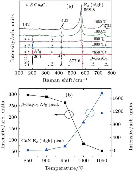
Fig. 3. Raman spectra of β-Ga2O3 film and the samples after nitridation at different temperatures for 0.5 h(a)and the curve of Raman peak intensity of the Ga2O3-A3g mode and the GaN-E2(high)mode with the nitridation temperature(b).
3.2. Analysis of nitridation time
Figure 4 shows the SEM images of as-nitridated β-Ga2O3films at 1050°C for different times. As the nitridation time is increased from 0.5 h to 3 h, the density and diameter of the hillock pits in the surface increase due to the enhancement of the β-Ga2O3decomposition. And a porous network layers forms obviously in the surface of sample after the nitridation.The above may result from that the β-Ga2O3film is dissociated and converted to GaN under NH3atmosphere.
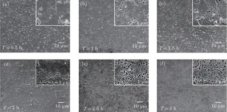
Fig.4. The SEM images of β-Ga2O3 films after nitridation at 1050 °C for different times. The insets are SEM images in the higher magnification.
Figure 5(a) shows the XRD patterns of as-nitridated β-Ga2O3films at 1050°C for different times. As is shown in Fig. 5(a), the XRD patterns contain strong diffraction peaks corresponding to GaN (002). And there are two weak peaks corresponding to β-Ga2O3in the sample nitridated at 1050°C for 1 h and 2 h. The appearance of β-Ga2O3peaks possibly be ascribed to the emerging non-surface layer of the β-Ga2O3film by nitridation. The XRD results reveal that the converted GaN films have a preferential orientation along (002) direction.
In order to characterize the crystal quality,the x-ray rocking curves (XRC) of the GaN (002) and (102) planes were obtained from as-nitridated β-Ga2O3films at 1050°C for different times. As shown in Fig. 5(b), the FWHM value of the GaN(002)and(102)plane remarkably decreases. The change of FWHM value indicates that the crystal quality of the GaN films becomes better with the increase of nitridation time because of the atom reconstruction during the nitridation process. The discrete FWHM value of GaN (102) may be attributed to the lack of N under a low NH3flow rate. The XRC results indicate that the converted GaN films show the singlecrystal structure and the nitridation time can improve the crystal quality of GaN films.
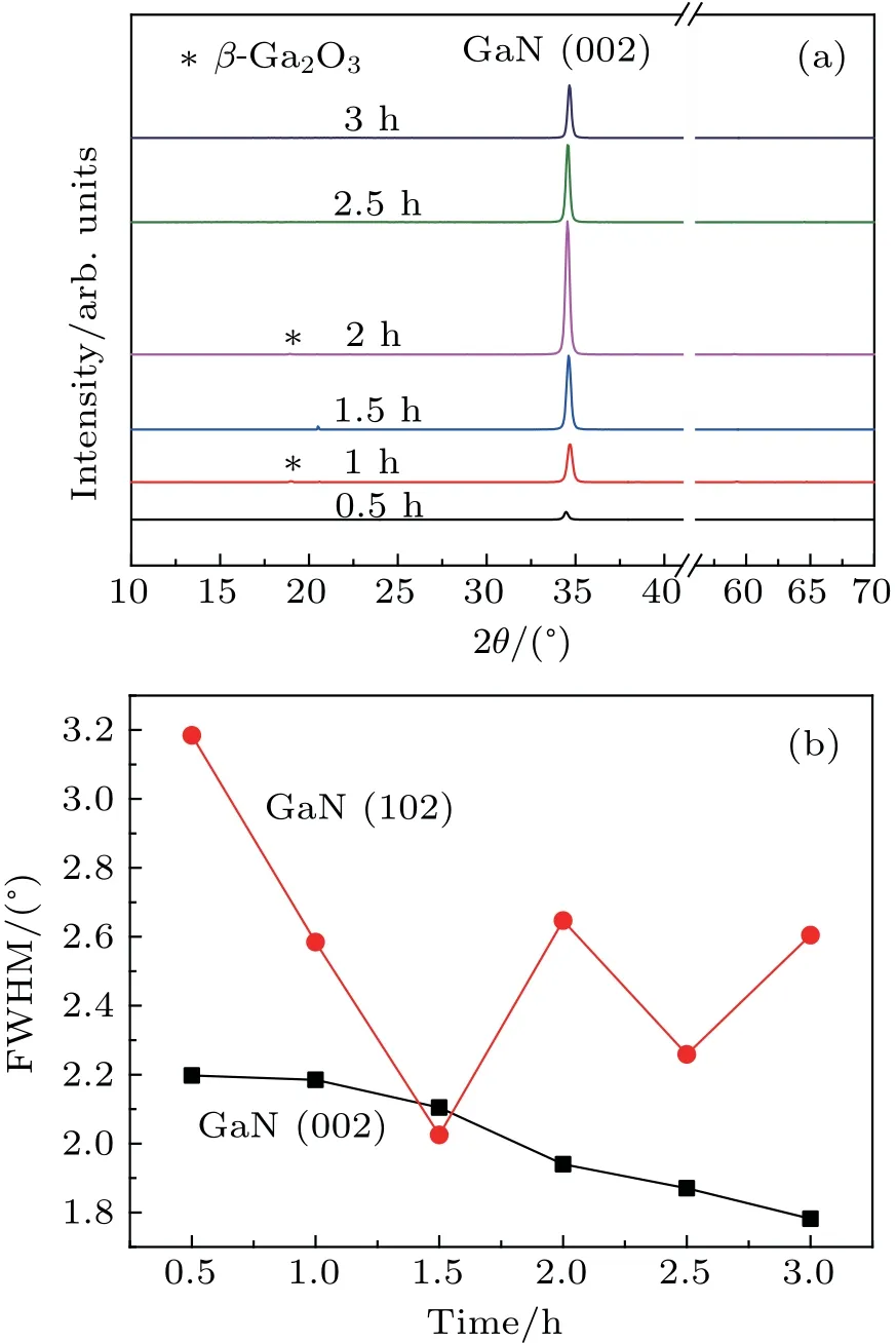
Fig.5. XRD patterns of β-Ga2O3 films after nitridation at 1050 °C for different times(a). The XRC patterns of GaN(002)and(102)formed at 1050 °C for different times(b).
Figure 6 illustrates the Raman spectra of as-nitridated β-Ga2O3films at 1050°C for different times. In addition to the phonon modes of GaN,the A3g phonon mode of β-Ga2O3is also observed in the spectra of as-nitridated films. And the peak intensity of the A3g phonon mode of β-Ga2O3gradually decreases until it disappears as the nitridation process proceeds. It should be noted that while the A3g phonon mode of β-Ga2O3is still observed, the E2(high) phonon mode of GaN shows a blue-shift,which indicates the existence of compressive stress in GaN. And the blue-shift offset of the E2(high) phonon mode is decreasing with the increase of nitridation time. As discussed earlier, the stress results from the incomplete conversion from β-Ga2O3to GaN. When the nitridation time increases to 3 h, the E2(high) peak is located at 567.7 cm-1with no blue-shift compared with that of bulk GaN, which means that there is no significant stress in GaN film nitridated at 1050°C for 3 h. So,it can be concluded that the enough nitridation time significantly improves the quality of GaN converted from β-Ga2O3,which is in accordance with the XRC analysis.
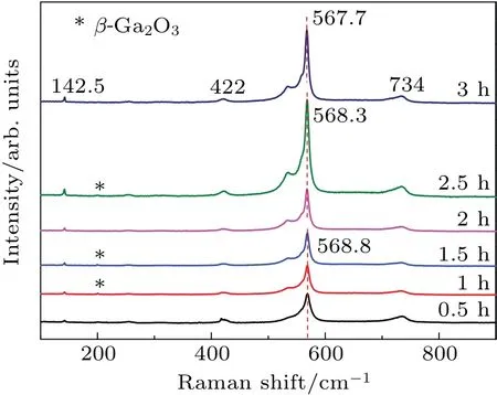
Fig.6. Raman spectra of β-Ga2O3 films after nitridation at 1050 °C for different times.
4. Conclusion and perspectives
In summary, GaN films have been obtained from the β-Ga2O3films by the nitridation under the NH3atmosphere.The nitridated films show a porous network surface morphology. The structural analysis indicates that the nitridated surface layer is single-crystal GaN layer. After full nitridation at 1050°C for 3 h, GaN layers show no significant stress. The nitridation temperature and time can promote and improve the crystal quality of GaN films. The porous GaN films obtained by the nitridation of β-Ga2O3can be used as templates for the epitaxial growth of GaN instead of the expensive bulk GaN substrates.
猜你喜欢
杂志排行

Chinese Physics B的其它文章
- Lorentz transmission electron microscopy for magnetic skyrmions imaging∗
- Spin transport in antiferromagnetic insulators∗
- First-principles study of the band gap tuning and doping control in CdSexTe1-x alloy for high efficiency solar cell∗
- Non-Stokes drag coefficient in single-particle electrophoresis:New insights on a classical problem
- SymTopo: An automatic tool for calculating topological properties of nonmagnetic crystalline materials∗
- Tunable coupling between Xmon qubit and coplanar waveguide resonator∗