Spin transport in antiferromagnetic insulators∗
2019-08-16ZhiyongQiu邱志勇andDazhiHou侯达之
Zhiyong Qiu(邱志勇) and Dazhi Hou(侯达之)
1Key Laboratory of Materials Modification by Laser,Ion,and Electron Beams(Ministry of Education),School of Materials Science and Engineering,Dalian University of Technology,Dalian 116023,China
2WPI Advanced Institute for Materials Research,Tohoku University,Sendai 980-8577,Japan
Keywords: spintronics,spin wave,antiferromagnetics,spin transport
1. Introduction
Spintronics emerged from discoveries in spin-dependent electron transport phenomena in solid-state devices. The significant event of spintronics was the discovery of giant magnetoresistance(GMR)independently by Albert Fert et al.[1]and Peter Gr¨unberg et al.;[2]this discovery is also considered the starting point of modem spintronics. Since then,spintronics,a new field of study at the intersection of magnetism,electronics and informatics,has gained considerable research attention in the science community.[3,4]In particular, since the beginning of the 21st century,spintronics has grown to be a separate field of research revolving around the fundamental term‘spin current’, in which transport phenomena of electrical spin and/or spin angular momentum have become central concepts. Extensive studies have been conducted on the use of spin current to replace charge current.[5]
Developing a pure spin-based device whereby information would be processed by spin rather than by charge,[5]has been a core mission for spintronics. Therefore, generation,modulation, and detection of spin are the three central issues in this mission, for which many approaches and new physics have been proposed, discovered, and discussed.[6]However,obtaining real applicable spin devices is still difficult, and achieving efficient spin modulation is the urgent issue. This study aims to find approaches and material systems to simply and efficiently control spin transport.
Basically, spin transport can be modulated by means of any spin-related interactions in a material, e.g., spin-spin,spin-phonon, and spin-photon interactions. As two sides of one entity,transport spins in a spin current can be used to probe spin-related properties of a material. Therefore,the spin modulation issue in a condensed-state system can be addressed by finding and fully understanding the interaction between spin and other degrees of freedom in a material.
Antiferromagnetics has become a growing concern in the field of spintronics. Recently, we have focused on antiferromagnetic insulators (AFMIs). First, spin-related phenomena and appropriate materials for next-generation spin-based devices can be extensively studied because of large number of AFMIs. AFMIs shield the spin transport from most associated charge-related effects, thereby making it easier to study the fundamental physics of spin angle-momentum transport. The demonstration of spin transport through an antiferromagnetic material was first achieved by Wang et al.,[7]and subsequently similar results were obtained by other researchers[8,9]using samples with comparable structure. Spins were injected into the AFMI layer using yttrium iron garnet(YIG)and detected by the inverse spin Hall effect (ISHE)[10]in platinum on the other side. The most interesting result of research using this YIG/AFMI/Pt structure is that the detected spin signal is enhanced when the AFM layer is NiO and the thickness is around 1 nm,[7]which motivated the development of spin-related investigations in AFMI.
We systematically studied spin transport phenomena in various AFMIs from the viewpoints of spin application and spin modulation. We found spin susceptibility and the N´eel vector to be the most important factors for spin transport in AFMIs. We summarize our experimental results and theoretical explanations. The remainder of this paper is organized as follows. Section 2 introduces the experimental set-up. Section 3 introduces our experimental results in three sub-sections, in which experiments related to spin susceptibility,[11]N´eel vector,[12]and spin colossal magnetoresistance (SCMR)[12]are described respectively. In the final section, we summarize our present work and discuss further challenges and potential applications.
2. Experiment set-up
Electron spin is not isolated but is correlated to many physical degrees of freedom,including spin itself. Therefore,other physical quantities can be probed via a spin-related interaction. Inelastic neutron scattering, for example, can be used to detect magnetic excitations in an antiferromagnetic system by spin-spin interaction between the neutrons’ spins and the local spins (Fig. 1(a)). In this process, the spin degree of freedom (rather than the particle of neutrons) is the only necessary element. This inspired our consideration that a pure spin-current may replace the neutron beam in this process, which in turn could reveal further related information(Fig. 1(b)). Two prerequisites are required to reproduce the inelastic neutron-scattering experiment in a spin-current way.First,a spin source is required to generate and inject spin currents into the target materials, which will replace the spins carried by a neutron beam. Second,an effective method is required to quantitatively detect spins passed through the target material.

Fig. 1. (a) The concept of the inelastic scattering of polarized neutrons.(b) The concept of spin-current transmission through an antiferromagnetic system.
Therefore, a trilayer device (Fig. 2) was developed, in which a target AFMI film was sandwiched between a magnetic YIG layer and a heavy metal Pt layer.In such a set-up,the single crystal YIG layer acts as the spin source layer,from which pure spin currents are injected into the adjacent target film.On the other side, Pt, the ISHE of which is relatively large,stable, and well-studied, detects the spin that passed through the target film. We set the trilayer device at the short termination of a short-end coplanar waveguide. By applying an external magnetic field and a microwave, ferromagnetic resonance (FMR) and a perpendicular temperature gradient are simultaneously excited in the YIG layer. Spin currents due to the spin-pumping effect and spin Seebeck effect (SSE)[13,14]are generated and injected into the adjacent target film. Then,the voltage signal due to the spin pumping and SSE can be observed simultaneously in a voltage spectrum from the Pt layer(Fig.2).
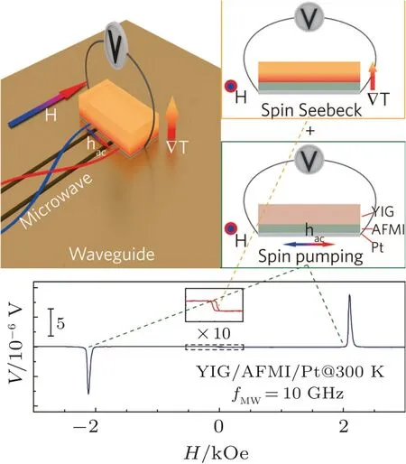
Fig. 2. Set-up of experiment using trilayer spin-transport device. The trilayer sample, built of yttrium iron garnet (YIG), antiferromagnetic insulators (AFMIs), and platinum (Pt), is placed near the short termination of a short-end coplanar waveguide. Ferromagnetic resonance in YIG is excited by an applied microwave,while a temperature gradient is created in the perpendicular direction. As a result,the spin-pumping effect and spin Seebeck effect can be observed simultaneously.
3. Experiment results and discussion
3.1. Spin susceptibility
Spin susceptibility is one of the key factors for spin transport in an antiferromagnetic system. The magnetic phase transition of an ultrathin antiferromagnetic film can be detected by a pure spin-current probe. The detection of such a phase transition in an ultrathin film is impossible without using large synchrotron facilities and a special x-ray magnetic linear dichroism spectrometer.[15-17]Our present method provides a way to probe such a phase transition by a bench-top experiment. Transport spins penetrating the antiferromagnetic film also carry the dynamic information about local spins due to spin-spin interactions. Potentially a method for magnetic re-search on ultrathin antiferromagnetic films,this approach will encourage further investigations.
Figure 3(a) shows spin pumping signals observed in a YIG/CoO/Pt trilayer device at various temperatures. Voltage peaks appear at the magnetic fields of FMR conditions.The signs of the peak voltages VISHEare reversed by reversing the polarity of the applied magnetic fields, showing that the voltage peaks are due to ISHE induced by spin currents pumped from the YIG layer. We chose a typical insulating antiferromagnetic film,CoO,was elected to be the target material, not only because the N´eel temperature of bulk CoO is ∼292 K[18,19]making our measurable temperature easily cover the antiferromagnetic transition region(given our physical property measurement system), but also because the excellent insulation property of CoO makes it easy to focus our research on the transport of pure spin currents.
Figure 3(c) shows the temperature dependence of the peak voltage VISHEof YIG/CoO/Pt trilayer devices,compared with that of a YIG/Pt bilayer (Fig. 3(b)). Clearly, unconventional peak structures appear in the temperature dependent ISHE signal VISHEwhile using an YIG/CoO/Pt trilayer device (Fig. 3(c), whereas VISHEdecreases monotonically with decreasing temperature while using an YIG/Pt bilayer device(Fig. 3(b)). The temperature dependences of VISHEfor samples with various CoO layer thickness have the same peak features, while sharing a shape like the temperature dependences of spin susceptibility for CoO films.[20]Peak temperature decreases with decreasing CoO-layer thickness, which is consistent with the finite size effect of ultrathin antiferromagnetic films.[20]The peak temperature of VISHEis comparable to the N´eel temperature of the CoO layer determined by an x-ray magnetic linear dichroism measurement using a synchrotron facility.[11]All the results show that the VISHEpeak position indicates the N´eel temperature of the CoO layer and that the VISHEenhancement around the antiferromagnetic transition can be related to the CoO-film spin susceptibility enhancement.The CoO layers in our samples are well controlled single-crystal structures with [111]directions along the outplane direction. When the spin currents are excited by SSE or CoO is replaced by other antiferromagnets,such as NiO film,similar peak structures can be observed in the temperaturedependent voltage signal(Fig.3(d)).The N´eel temperature determined in YIG/AFMI/Pt trilayer devices should be the magnetic ordering temperature of AFMI layer under the effect of the magnetic YIG layer.[21]
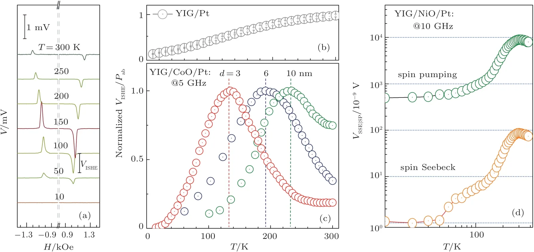
Fig.3. (a)Magnetic-field(H)dependence of electric voltage(V)generated in YIG/CoO(3 nm)/Pt trilayer film at various temperatures. VISHE denotes the voltage signal in the ferromagnetic resonance field. (b)Temperature dependence of VISHE for the YIG/Pt bilayer film. (c)Temperature dependence of VISHE for the YIG/CoO(3,6,10 nm)/Pt trilayer devices. (d)Temperature dependence of spin pumping signal VSP and spin Seebeck signal VSSE for the YIG/NiO(1.5 nm)/Pt trilayer devices.
These results indicate that the spins are transported dominantly by incoherent thermal magnons rather than coherent N´eel dynamics in an antiferromagnetic system. At high temperatures, thermal magnons continuously evolve into thermal spin fluctuations,which would transport spin current above the N´eel temperature.Such thermal spin dynamics both below and above TNare well described by the bosonic auxiliary-particle method.Using this method,the spin conductivity in an antiferromagnetic insulator was shown to be maximized near its N´eel temperature, exactly like our VISHE.[22]Since VISHEmeasures spin moments transferred across magnetic insulators, its enhancement directly reflects that of the spin conductivity. The spin conductivity and the magnetic susceptibility are in principle different quantities. However, their temperature dependence is rather similar because both are dominated by spin excitations with zero momentum transfer. Therefore,VISHEin our experimental set-up is a good measure of spin dynamics and transition.
3.2. N´eel vector
Unlike electrical charge,spin has not only a definite magnitude but also has a ’direction’, which makes spin transport act with an intrinsic anisotropy. It is natural that magnetic anisotropy affects the spin transport in condensed-state matter. In an antiferromagnet system, the magnetic anisotropy is mainly defined by the N´eel vector. In Fig. 4(a), we show the crystal and spin structure of another antiferromagnetic insulator Cr2O3. In Cr2O3, there is only one easy axis pointing to the c axis of a hexagonal structure. We prepared trilayer samples,in which this time the middle target layer was Cr2O3(Fig. 4(b)). The crystal orientation of Cr2O3was carefully controlled to ensure that the c axis was perpendicular to the surface of the device. This means the N´eel vector direction can be different from the spin accumulate direction. SSE was used to inject spin currents from the YIG layer into the Cr2O3.Spin currents,passed through the Cr2O3layer,were converted into a measurable voltage in the Pt layer via the ISHE.
Figures 4(c) and 4(d) show the magnetic-field dependence of the measured voltage V for a YIG/Pt device and a YIG/Cr2O3/Pt device. The YIG/Pt device was used as a control sample because the SSE has been extensively studied in this bilayer system. In both samples - with and without a Cr2O3layer-the sign of V reverses with the sign of H,and the shape of the V-H curves agree with the M-H (hysteresis)curve of the YIG film.[23-25]This confirms that the measured voltage V in the YIG/Cr2O3/Pt trilayer device is induced by the thermal spin currents generated from the YIG via SSE.
A steep conductor-nonconductor transition for spin currents was observed in Cr2O3. Figure 4(e)shows the temperature dependence of the SSE voltage VSSEfor the YIG/Cr2O3/Pt trilayer device. Unexpectedly,the voltage exhibited an abrupt change of more than 100× at ∼290 K. Above this temperature,a peak voltage appears at T =296 K.When T <282 K,VSSEis close to the noise floor(Fig.4(e)). By contrast,in the YIG/Pt bilayer device,VSSEvaries little across the same temperature region(Fig.4(f)).[26]The abrupt change ofVSSEin the YIG/Cr2O3/Pt marks the transition of the Cr2O3layer from a spin conductor to a spin nonconductor at T =296 K. This critical temperature coincides with the N´eel temperature of the Cr2O3thin film.[27,28]We found a similar spin conductornonconductor transition in a spin-pumping measurement for devices with the same YIG/Cr2O3/Pt structure as shown in Fig.4(g),demonstrating that the spin conductor-nonconductor transition in Cr2O3does not depend on the method of spincurrent generation. By using a control sample with a 5-nm Cu layer inserted between the YIG and Cr2O3layers (Fig. 4(h)),we also ruled out magnetic interface effects between the exchanged coupled YIG and Cr2O3(such as exchange bias,proximity effect or spin-reorientation transitions)as the cause of the large change in VSSE. By measuring the VSSEwhen using a Cr2O3/Pt bilayer sample, we also confirmed that VSSEcomes from the spin current generated in the YIG and transmitted through the Cr2O3rather than by spin currents originating within Cr2O3or from a Nernst effect in a magnetized Pt layer(Fig.4(h)).

Fig. 4. (a) Schematic diagram of the crystal structure of antiferromagnetic Cr2O3. (b) Cross-sectional transmission-electron microscopy image of the YIG/Cr2O3/Pt trilayer device used in this research. Scale bar represents 5 nm. Easy axis c of Cr2O3 is in the film’s out-of-plane direction z. (c)External magnetic field HHH dependence of voltage signal V measured in YIG/Pt bilayer device at 300 K.(d)External magnetic field HHH dependence of voltage signal V measured in YIG/Cr2O3/Pt trilayer device at various temperatures.(e)Temperature dependence of spin Seebeck voltage VSSE at H=0.1 T for YIG/Cr2O3/Pt trilayer device. Inset shows concept of spin-current transmissivity measurement. (f)Temperature dependence of spin Seebeck voltage VSSE at H=0.1 T for a YIG/Pt bilayer device. (g)Temperature dependence of spin pumping signals VISHE for YIG/Cr2O3/Pt trilayer devices with various values of Cr2O3 layer thickness dCr2O3. (h)Temperature dependence of spin Seebeck voltage VSSE at H=0.1 T for YIG/Cu/Cr2O3/Pt and Cr2O3/Pt devices.
The sharp transition observed at the N´eel temperature is attributed to the anisotropic transmissivity of the antiferromagnet in combination with the device geometry. Above the N´eel temperature, the paramagnetic moments of Cr2O3follow the external magnetic field and spin current is carried by the correlation of the paramagnetic moments as previously reported.[11,29,30]Below the N´eel temperature, in the ordered antiferromagnetic phase,only the spin component parallel (or antiparallel) to the N´eel vector can be carried by magnons.[31]Below the N´eel temperature, due to the strong uniaxial anisotropy,the N´eel vector of Cr2O3is pinned to the easy axis (out of plane in this work). When the YIG magnetization is in the plane of the film, the spins are polarized perpendicularly to the Cr2O3N´eel vector and the spin current cannot be transmitted into the Cr2O3. Also, the strength of the anisotropy in Cr2O3is almost independent of temperature,collapsing to zero only very close to the N´eel temperature.[32]Therefore, the Cr2O3is strongly aligned perpendicular to the plane for almost the entire temperature range and no spin current can be transmitted. The small temperature window where the anisotropy decreases corresponds with the increase in ISHE voltage.
3.3. Spin colossal magnetoresistance
Colossal magnetoresistance (CMR) refers to a large change in electrical conductivity induced by a magnetic field in the vicinity of a metal-insulator transition. CMR occurs due to a correlation between the magnetic structure and electron conduction and has inspired extensive studies for decades.[33,34]As mentioned above, we have confirmed the spin conductor-nonconductor transition in the Cr2O3antiferromagnetic system. If the spin conductivity of such a system can be tuned by an external magnetic field, we then can term a spin version of CMR effect(SCMR).We found that the spin conductivity of Cr2O3has an anisotropic response to magnetic fields in the critical region of the magnetic transition and that it depends on both the magnitude and direction of the magnetic field.
Within the critical region, we measured the dependence of VSSEon the magnetic field magnitude |HHH| and angle θ in the z-y plane (Figs. 5(a) and 5(d)). At T = 296 K (in the spin conducting regime),VSSEshows a sinusoidal change with respect to θ. The magnitude of VSSEchanges only slightly from |HHH|=0.5 T to 2.5 T. Similar behavior is observed for T >296 K.However,at T <296 K,VSSE(θ)starts to deviate from this dependence. As the temperature decreases further,the character of VSSE(θ)changes completely,the shape changing to resemble rabbit ears in polar coordinates of θ. VSSEalso becomes strongly dependent on |HHH|. Thus,VSSE(θ, H)depends on both θ and|HHH|in the critical region.

Fig. 5. (a) Out-of-plane spin Seebeck set-up for the YIG/Cr2O3/Pt trilayer device. Temperature gradient, ∇T, is along the z direction, and an external magnetic field,HHH,is applied in the y-z plane. θ is the angle between ∇T and HHH. (b)θ dependencies of VSSE at different temperatures for the YIG/Cr2O3/Pt trilayer device for various values of HHH. (c) External magnetic field HHH dependence of voltage signal V measured in the YIG/Cr2O3/Pt trilayer device for θ =20° at various temperatures. (d) Temperature dependence of VSSE for the YIG/Cr2O3/Pt trilayer device for different external magnetic fields HHH at θ =20°. Solid lines serve as visual guides. (e)Ts change ratio Ratio(Ts)@H due to external magnetic fields HHH as functions of temperature. Ratio(Ts)@H=(VSSE@H-VSSE@0.5 T)/VSSE@0.5 T. Ts refers to spin-current transmissivity in the Cr2O3 layer. Solid lines serve as visual guides.
Figure 5(d) shows the temperature dependence of VSSE(|HHH|) at θ = 20°, where the |HHH| dependence is the most pronounced(Fig.5(c)). The temperature dependence of VSSEis qualitatively similar for all field strengths, featuring a sharp transition between the spin nonconductor and conductor regimes. However, the transition edge of VSSEshifts to lower temperatures for stronger magnetic fields. Taking|HHH|=0.5 T as a reference,∼500%modulation of VSSEis achieved with a 2.5 T field(Fig.5(e)).
As mentioned in the prior section, only the spin component parallel(or antiparallel)to the N´eel vector can be carried by magnons,therefore spin transport is blocked because of the strong uniaxial anisotropy. However,in the region just below the N´eel temperature,where the anisotropy is reducing,the enhanced susceptibility and reduced anisotropy in this small temperature window allows the N´eel vector to be slightly rotated.giving a finite in-the-plane y-component onto which the spin current is projected.[32,35]This makes spin conductivity able to be manipulated with an applied magnetic field: the SCMR.
4. Summary
From results of our investigating spin-transport phenomena in various AFMI thin films, we found that the spin susceptibility and the N´eel vector are the most important factors affecting the transport spin. We demonstrated that spin current can be a probe for detecting the antiferromagnetic phase transition in an ultrathin AFMI film. Furthermore, in a uniaxial AFMI Cr2O3, we discovered a spin conductor-nonconductor transition. Such a transition can be tuned efficiently by an external magnetic field;as it is reminiscent of the CMR in electronics,we call it the spin CMR(SCMR).
Our results show that the AFMI system is a possible functional core for a spin device, by which a spin transistor may be achieved.[36]However, the mechanisms of spin transport through AFMI,which is indispensable for further design and development of such a device,has not been clarified. For example,the frequency dependence of the spin-pumping behavior near the N´eel temperature,[11]which implies that the observed phenomena reflects dynamical properties, is required for further theoretical understanding. Therefore,constructing a comprehensive theory for spin-current transport is an important outstanding task for the future development of the proposed spintronic device based on AFMI.
杂志排行

Chinese Physics B的其它文章
- Lorentz transmission electron microscopy for magnetic skyrmions imaging∗
- First-principles study of the band gap tuning and doping control in CdSexTe1-x alloy for high efficiency solar cell∗
- Non-Stokes drag coefficient in single-particle electrophoresis:New insights on a classical problem
- SymTopo: An automatic tool for calculating topological properties of nonmagnetic crystalline materials∗
- Tunable coupling between Xmon qubit and coplanar waveguide resonator∗
- Efficient solver for time-dependent Schrödinger equation with interaction between atoms and strong laser field∗