Progress in quantum well and quantum cascade infrared photodetectors in SITP∗
2019-02-25XiaohaoZhou周孝好NingLi李宁andWeiLu陆卫
Xiaohao Zhou(周孝好),Ning Li(李宁),and Wei Lu(陆卫)
State key Laboratory for Infrared Physics,Shanghai Institute of Technical Physics(SITP),Chinese Academy of Sciences,Shanghai 200083,China
Keywords:infrared photodetectors,quantum well,focal plane array,detectivity,broadband response
1.Introduction
Quantum well infrared photodetectors are based on intraband optical transitions between the subbands in quantum heterostructures and take benefits from the band engineering.[1-4]QWIPs based on lattice matched GaAs/AlGaAs material system,which is famous for its mature growth and processing technology,have been studied in detail and have already been used in large format FPAs.[5]QWIPs have been widely investigated for detection in the mid-wavelength(MW,3µm to 5µm),long wavelength(LW,8µm to 12µm),and very long wavelength(VLW,> 12µm)infrared atmospheric spectral window.Thanks to the tunability of the quantum heterostructures(alloy composition,layer thickness,etc.),QWIPs have been demonstrated from 3µm to 80µm.[6]Detailed reviews about QWIPs can be found in references.[7,8]
The main working mechanism of QWIPs involves the transition between the ground state and the first excited state.The first QWIP based on bound-to-bound(BTB)state transition with a narrow bandwidth(10%)photosensitivity was demonstrated in 1987,as shown in Fig.1(a).[4]Since the excited bound state is far below the top of the barrier,the photoexcited carriers in BTB QWIPs need a rather large working bias to escape out of the well under illumination.A large working bias will give rise to a large dark current,which deteriorates the device performance accordingly.Coon and Karunasiri proved that QWIPs have better performance when the first excited state lies just above the threshold of the conduction band.[2]By decreasing the quantum well width,the excited bound state can be pushed up into the continuum,resulting in a significantly stronger bound-to-continuum(BTC)state absorption,as shown in Fig.1(b);thus,the detector can generate a photocurrent at a very low bias.[9]In short,the location of the first excited state relative to the top of the well can have a dramatic effect on device performance.Optimizing QWIP performance primarily focuses on two factors:improving the response photocurrent and minimizing the dark current.Both of these factors have a close relationship with the position of the first excited state.In order to achieve better performance,the first excited state is usually designed to be resonant with the conduction band of the barrier,which is expected to have a bound-to-quasi-bound(BTQB)state transition mode rather than that of the BTC and BTB types.However,it is not always easy to grow material in which the first excited state is exactly at the well top,and sometimes the first excited state is a few meV below the conduction band edge of the barrier.Meanwhile,when we design the QWIP structure to get BTQB state transition,we often assume the conduction band is flat.In reality,the conduction band will be affected by the doping density,working temperature and bias,especially when the first excited state is very close to the band edge.

Fig.1.Two possible configurations for the optical transition.(a)Bound-to-bound;(b)Bound-to-continuum.
Following QWIPs,quantum cascade detectors(QCDs)have been investigated widely as a photovoltaic alternative to the intrinsically photoconductive QWIPs.[10]In this case,the electrons in the excited state are not extracted to the next period through the continuum but they cascade to the next module ground state via a series of phonon ladders,as shown in Fig.2.

Fig.2.Active region of a quantum cascade detector.
QCDs can be fabricated via different material systems such as GaAs/AlGaAs,[11,12]InGaAs/InAlAs,[13,14]GaN/AlGaN.[15,16]With various designs,the detection of QCDs had already covered the wavelength ranging from the near infrared to THz.QCDs are photovoltaic devices which can operate at zero-bias condition with low dark current and low noise.These characteristics make QCDs more suitable for infrared imaging,solution analysis and gas sensing.[17-19]As a BTB intraband transition detector,the linewidths of QCDs are really narrow.Hence,common QCDs cannot be applied in broad spectral detection,such as infrared spectroscopy,hyperspectral and space applications,etc.[20]To improve the spectral breadth of QCDs,a few different approaches have been proposed.For example,using a stack of active heterostructures where each stack covers a particular wavelength.Hofstetter et al.had reported a mid-infrared QCD,ranging from 4.7 µm to 7.4 µm,with the spectral breadth ΔE/E=27.3%.[13]However,this design is complicated and the responsivity spectrum is sensitive to temperature.Recently,the conceptofdiagonaltransition in the active region was also presented to demonstrate a broadband mid-infrared QCD.[21]But the state-of-the-art diagonal transition design cannot balance the high responsivity and the wide spectral breadth.[22]
In this review,we will discuss the recent progress on QWIPs and QCDs in SITP,CAS.In Section 2,we mainly clarify how the bias and temperature affect the first excited state that is located a few meV below the conduction band edge of the barrier in VLW QWIPs,and present a double-excited state model to explain the wavelength shift with bias and temperature.In Section 3,the VLW QWIP(its cutoff wavelength is larger than 16µm)FPA with 320×256 pixels based on BTQB design has been demonstrated.The technology of the manufacturing FPA based on the QWIPs and the imaging performance are also summarized.Subsequently,a novel broadband QCD is proposed for long wavelength infrared detection via the coupled quantum wells design,which covers the wavelength range from 7.6 to 10.4µm with a relative linewidth of 30.7%and the spectralshape and linewidth can be tuned by the thickness of the thin barrier.Lastly,we provide a perspective on the opportunities and challenges in this research area.
2.VLW QWIPs with the double excited states
2.1.Experimental details
In order to illustrate how the different excited states in a QWIP in fluence its device performance,we designed two typical QWIPs based on the GaAs/AlxGa1-xAs material system using the BTQB and BTQC,respectively.[23]Two QWIP samples,labeled as 522#and 524#were grown on(100)-oriented semi-insulating GaAs substrates by means of molecular beam epitaxy.The multiple quantum well(MQW)structure consists of 50 periods of a GaAs well(which is n-doped at 2.5×1017cm-3)and an Al0.12Ga0.88As barrier.The MQW is sandwiched between a 1.75-µm GaAs top layer and a 1.2-µm bottom contact layer.Both layers are n-type doped at 2.5×1017cm-3.The barrier widths of the two samples are 60 nm.The only difference between the two samples is the well width,which are 8.0 nm and 7.3 nm for samples 522#and 524#,respectively.After growth,the wafers were processed into square-shaped mesas of size 200µm×200µm using standard photolithography and wet etching.Ohmic contact was deposited by AuGe/Ni/Au.A 45°multipass waveguide was polished in order to couple light into the active region.The sample was then soldered on to a copper heat sink and placed in a closed cycle helium cryostat.The blackbody response measurementswere performed by using a 500-Kblackbody source with a chopping frequency f=173 Hz,a SR 570 low-noise current amplifier,an SR 830 lock-in amplifier,and a Keithley 236 source measure unit at 50 K.
2.2.Individual detector performance
2.2.1.Blackbody response and photocurrent spectra
Figure 3 presents the relationship between the blackbody response and the bias voltages for samples 522#and 524#.In comparison to Sample 524#,the blackbody response current versus bias for 522#is nonlinear.This nonlinear behavior indicates that the first excited state of sample 522#is below the well top because electrons in the excited state require a larger electric field to assist to escape out of the well via tunneling.[24]
The photocurrent spectra of the samples were measured with a Fourier transform infrared spectrometer(Nicolet 6700)at 10 K and 50 K,as shown in Fig.4.The photocurrent spectra of the two samples at 10 K are both flat at a lower bias.The peak positions(λpeak)of the photocurrent spectra of samples 522#and 524#measured at 0.2 V are about 12.7µm and 13.7 µm,respectively.When the bias is increased,the λpeakof the detectors shifts to longer wavelengths.Once the bias is greaterthan 0.5 V,theλpeakofthe detectorsremain unchanged.
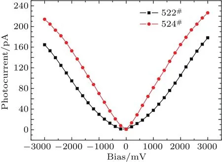
Fig.3.Blackbody response of samples 522#and 524#at a 500-K source with a chopping frequency of 173 Hz.[23]

Fig.4.Spectral response curves for(a)sample 522#and(b)sample 524#with different biases at 10 K.Spectral response curves for(c)sample 522#and(d)sample 524#with different biases at 50 K.A dashed line is drawn following the peak position as a guide for the eye.[23]
Note that with an increase of the bias,the full width at half-maximum(FWHM)Δλ of the two samples both decreases.The Δλ/λ (%)of 522#decreases from 40%at 0.2 V to 15.2%at 0.9 V,while the Δλ/λ (%)of 524#decreases from 35%at 0.15 V to 15.4%at 1 V.The obvious change in Δλ/λ (%)indicates that the transition mode changes as the bias increases.Another difference between 522#and 524#is the threshold voltages at which the peak wavelength stops a shift.The peak wavelength shift of 522#primarily occurs at a bias level around 0.35 V,while that for 524#primarily happens at around 0.25 V.Compared with Figs.4(a)and 4(b),the obvious difference in Figs.4(c)and 4(d)is that the peak positions of the photocurrent spectra do not shift as the bias changes at 50 K.At 10 K,the thermal energy kBT is 0.86 meV,while at 50 K the thermal energy increases to 4.3 meV.It is clear that the increase in thermal energy will lead to the redshift of the peak response in the photocurrent spectra.
2.2.2.Double-exited states model
The energy difference between the ground state and the first excited state usually determines the peak wavelength of intersubband transitions and only the first excited state is considered to be the crucial factor.However,for QWIPs based on BTQB state transition,a model of the single excited state cannot explain the redshift of the spectral response as the bias and temperature change.Therefore,the excited states in the continuous state cannot be ignored,especially when the QWIPs work at a very low temperature and bias.Based on this understanding,a double-excited states model is proposed to explain the redshift of the spectral response.Figure 5 presents the diagrams of the single-and the dual-excited state models for comparison.

Fig.5.Band diagrams of(a)the single excited state model and(b)the dual excited states model.When the first excited state is below the well top,the carriers in the first excited state have two ways to generate photocurrent: field assist tunneling and thermal emission.
According to the basic principle of intersubband transitions,the optical current Iphcan be written as,[6]

where e,φ,pe,α,L,gph,and R represent electron charge,incident photo flux,escaping rate that electrons escape from quantum wells to barriers,light absorption coefficient,active length in the device,photoconductive gain,and surface equivalent reflectivity of the device,respectively.There are only two voltage-dependent parameters in Eq.(1):peand gph.As shown in Fig.5(b),two intersubband transitions happen after electrons in the ground state absorb photons.One transition is from the ground state to the first excited state and the other one is from the ground state to the excited state in the continuum.The absorption coefficient of the former transition is larger as the transition matrix is larger.Although the absorption coefficient of the latter transition is smaller,once the electron is transmitted to the continuous state,it can easily form a photocurrent accelerated by an electric field without tunneling through the triangle barrier.By means of the field assisted tunneling,the first excited state carrier can escape to the barrier to form a photocurrent.As a result of the field assisted tunneling,the photocurrent from the first excited carrier gradually dominates the spectrum.That means the quasi-bound state will be converted into the quasi-continuum state as the bias changes.
In order to prove that the increase of temperature will enhance the escape rate of electrons in the first excited state,and thus cause the redshift of the peak response in the photocurrent spectra,we have measured photocurrentspectra ofthe samples at a very small bias.Figure 6 shows the photocurrent spectra of the two samples at the bias of0.15 V.It can be seen thatboth peak positions of the photocurrent spectra of the samples shift to lower energy when the temperature increases.The escape rate for the first excited state carriers to escape to the barriers is closely related to the temperature.With the increased temperature,more carriers in the first excited state will escape to the barrier instead of being trapped and returned back to the ground state.By means of thermal ionization,the photocurrent from the first excited state carriers gradually dominates in the spectrum.
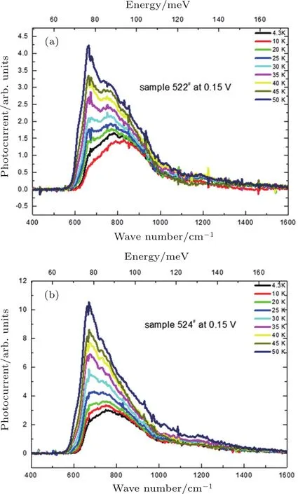
Fig.6.Spectral response curves for samples 522#and 524#at different temperatures with a 0.15-V bias.[23]
In fact,the normalized photocurrent spectra induced by the intersubband transitions do not change as the temperature and bias change.It is the intensity change of the normalized photocurrent spectra that causes the whole photocurrent spectra to be different at different biases and temperatures as pre-sented in Fig.4.Thus,we can separate the photocurrent spectra into two components,Iph1and Iph2,which arises from the excitations from the ground state to the first excited state and the ground state to the excited state in the continuum,respectively.The photocurrent spectra can therefore be expressed as a combination of these two normalized photocurrent spectra as

where k1,k2represent the proportion of Iph1and Iph2in the whole photocurrent Iph,respectively.The peak wavelength energy of Iph1is lower than that of Iph2,so the high energy part of the photocurrent spectra is mostly attributed to Iph2.Here,we take sample 522#as an example.In the photocurrent spectra at 0.2 V,k1is smaller than k2due to the small escape rate of the first excited state carriers.Correspondingly,the larger component of the photocurrent spectra originates from Iph2.At the bias of 0.2 V,the energy peak of the photocurrent spectra is about 788 cm-1and the full width at half maximum Δλ is about 284 cm-1,so Δλ /λ (%)≈ 36%;this is a typical transition from the ground state to the continuum excited state.At a higher bias(0.9 V),the field assisted tunneling process of the first excited state becomes easier and therefore Iph1increases more quickly than Iph2.The energy peak of the photocurrent spectra is about 664 cm-1and its FWHM Δλ is about 107 cm-1,so Δλ /λ (%)≈ 16%.Both the redshift of the peak wavelength and the decrease of the FWHM indicate that the transition from the ground state to the first excited state in sample 522#is dominant in the photocurrent spectra.In order to extract Iph1and Iph2from Iph,we assume that the part above 830 cm-1in photocurrent spectra is mostly attributed to Iph2.As the escape rate of the excited state carriers in the continuum is approximate to 1,the photoconductive gain will increase proportionally as the bias increases.This means that the intensity of the photocurrent spectra above 830 cm-1will increase proportionally as the bias increases.So,we can use the data above 830 cm-1in the photocurrent spectra at 0.8 V multiply a factor which is equal to 0.9/0.8 and use the data at 0.9 V to reduce the former result.From this,we get the photocurrent spectrum which is due to the transition from the ground state to the first excited state.The spectrum after normalization is shown by the black line in Fig.7.In addition,the part of photocurrent spectra below 620 cm-1is mostly attributable to Iph1.We use the same method to get the normalized photocurrent spectrum Iph2,which is also shown by the red line in Fig.7.

Fig.7.Normalized photocurrent spectra arise from the excitations from the ground state to the first excited state I ph1(black line)and the ground state to the excited state in the continuum I ph2(red line).[23]
2.2.3.Dark current and detectivity
Figure 8(a)presents the measured dark currents for 522#and 524#at 50 K.It is shown that 522#based on BTQB has a lower dark current than that of sample 544#that based on BTQC.According to the definition of the peak detectivity,[7]
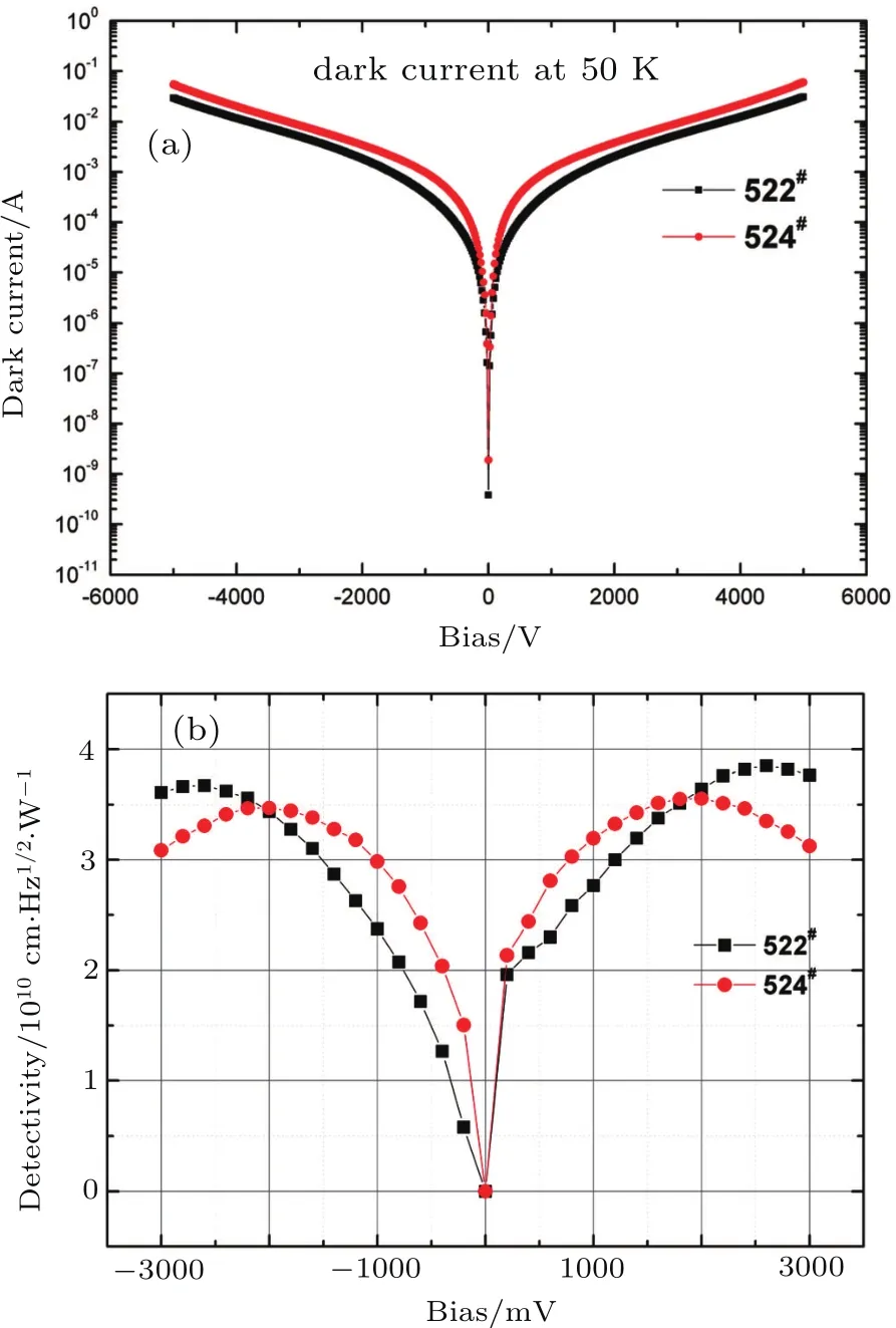
Fig.8.(a)Dark currentofsamples522#and sample 524#at50 K.(b)Plotof detectivity versus bias voltage for sample 522#and sample 524#at 50 K.[23]
where R is the peak responsivity,A is the area of the detector,in is the dark current noise and Δf is the band width(taken as Δf=1 Hz).We plot the detectivity versus the bias voltage in Fig.8(b).The peak detectivity of 522#is 3.85×1010cm·Hz1/2/W at 2.6 V,larger than the peak value 3.55×1010cm·Hz1/2/W of 524#at 2 V.Notice that in the bias ranges of-2 V to 1.8 V,the detectivity performance of 524#is better than that of 522#.In contrast,at a higher bias,the detectivity of 522#is higher.Though the blackbody response of 524#in Fig.3 is larger than 522#,the larger dark current of 524#limits the ultimate detectivity performance.Therefore,when designing the structure of QWIPs,one has to make a trade-off between a larger photocurrent and a smaller dark current.Our results show that the device performance when the first excited state is more confined within the well is a little better than when the first excited state is less confined within the well.In order to get better device performance,our suggestion is that the energy difference between the first excited state and the barrier edge with no bias voltage should be larger than the thermal energy kBT at a certain temperature.
3.VLW QWIP FPAs
Large format QWIP FPAs using a GaAs/AlGaAs materials system have been developed for infrared imaging applications.Currently,there is a great interesting in long wavelength infrared QWIPs due to IR imaging systems that require large area,uniform FPAs for a wide variety of applications,including night vision,tracking,navigation, flight control,early warning systems,earth resource observation,astronomy,and medical diagnosis etc.[5,25,26]In this section,the VLW GaAs/AlGaAs QWIP FPAs on the basis of the BTQB design were demonstrated by the technological operations based on photolithography,etching processes,and hybridization with silicon read out integrated circuits(ROICs).The technology development was carried out at the FPA with 320×256 elements with a 30 microns pitch.
3.1.Formation of the diffraction grating
An n-type GaAs/AlGaAs QWIP does not have any significant photoresponse when the light incident is normal to the well.Thus,a two-dimensional(2D)diffraction grating with the parameters determined by the spectral range and properties of the dielectric applied is required to provide the absorption of a normal-incident light for the QWIPs.[27]The required etching depth d is determined by the relation d=λ/4n,where λ is the radiation wavelength and n is the refractive index of the GaAs.These parameters are λ =14 µm∼ 15 µm and d=1.4µm for the wavelength range applied.The period of the diffraction grating L=4.8µm∼5.0µm was chosen.The diffraction grating and mesa structures were formed by dry anisotropic etching in a remote gas-discharged plasma(ICP RF)of the SiCl4,argon,and nitrogen.The obtained diffraction grating holes are square shaped with rounded corners and vertical walls,seeing Fig.9(a).The view of the mesa structure walls formed by etching the GaAs at a given depth is also shown in Fig.9(b).
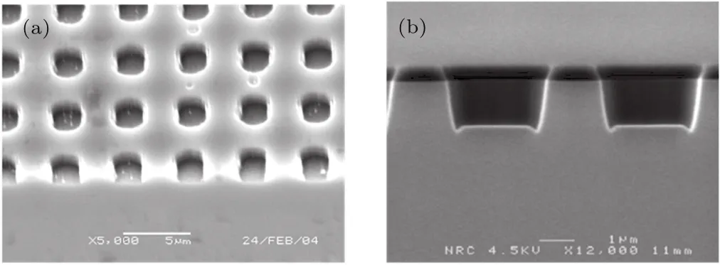
Fig.9.SEM images of(a)the diffraction grid and(b)the gap between the mesa structures of the FPA 320×256 elements obtained by dry etching.
3.2.Hybrid assembly of the FPA
The ohmic contacts to the base and upper n+-doped GaAs layers(on the mesa surface)were fabricated by the AuGe/Ni/Au deposition after the removal of the native oxide layer from the semiconductor surface by HCl:H2O(1:8)and annealing in a hydrogen.To assemble an FPA by cold welding,indium bumps were fabricated both on the GaAs/AlGaAs QWIP structure and silicon multiplexers.The photoresist was used to produce indium bumps by inverse photolithography.The view and cleavage of a separate mesa structure with an indium bump of the FPA with 320×256 elements produced by the GaAs/AlGaAs QWIP is shown in Fig.10.
The FPA modules were assembled by cold welding of the indium bumps under pressure.The fusion of the indium contacts was performed by heating the module up to the indium melting temperature with the succeeding cooling.The surface auto-planarization is provided during the crystal compression process.The total height of the indium bumps after the FPA assembly is optimized,which satis fies the requirements of the durability of the FPA hybrid assemblies.In order to diminish the strain and reduce the dark current,the substrate needs to be removed.The technology of the substrate removal after the assembly of the FPA includes mechanical grinding aimed at removing the main thicknessofthe substrate and chemicalmechanical polishing.The picture of the FPA after the removal of the GaAs substrate is shown in Fig.11.

Fig.11.The photo of the QWIP FPA on a leadless-chip-carrier after removing the substrate.
3.3.Opto-electronic characteristics of the FPA assembly
At the final stage,the opto-electronic characteristics of the fabricated FPA assembly were determined.For this purpose,the assembly was placed in a helium cryostat with an entrance window made of the ZnSe.A typical spectrum of photosensitivity of a 320×256 FPA is shown in Fig.12.The spectral width and the cutoff wavelength are 4.6µm and 16.2µm,respectively.Two examples of the infrared imaging detected by a 320×256 FPA are shown in Fig.13.
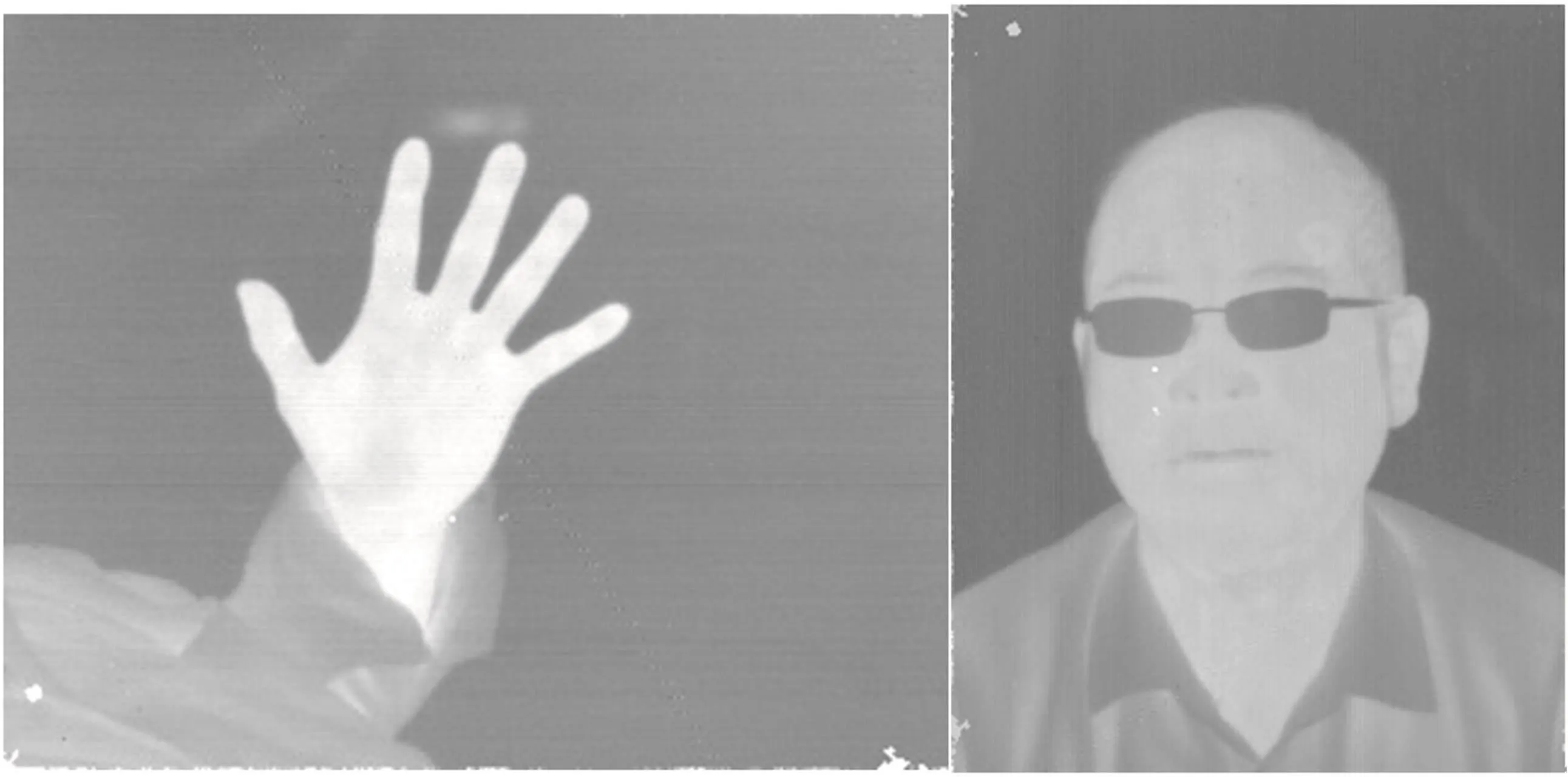
Fig.13.Images taken with the VLW QWIP FPA.The temperature is 45 K and the integration time is 2 ms.
3.4.Integrated detector cooler assembly
The fabricated and tested 320×256 FPA were installed in the body of a vacuum cryostat integrally coupled with a Stirling-type pulse tube cryocooler.The resulting integrated detector cooler assembly(IDCA)is shown in Fig.14.A vacuum cryostat performs thermal isolation of the array from the environment to guarantee effective cooling of the photodetector up to the operating temperature(T=35 K-50 K).The radiation from the detected objects is fed to the FPA through a window made up of ZnS with the antireflection in the range of 14µm-16µm and a cooled diaphragm with a relative aperture F/2 designed to reduce the background illumination.Typical operating temperatures for the FPA based on the QWIP with the wavelength range 14µm-16µm are 35 K-50 K.Thus,the Stirling-type pulse tube cryocooler ensured a cooling capacity at an operating temperature of 45 K not less than 1 W.

Fig.14.The photo of the QWIP IDCA integrated detector cooler assembly.
As one can see from Table 1,the parameters of the developed 320×256 QWIP IDCA are comparable with those of the Jet Propulsion Laboratory,USA.[28]
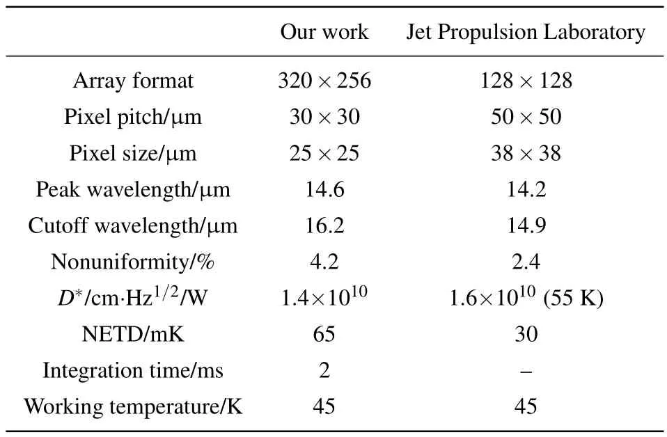
Table 1.Comparative characteristics of the QWIP FPAs by SITP,CAS and Jet Propulsion Laboratory.
4.LW broadband QCD
4.1.Broadband QCD design
QCDsare usually designed to contain severalperiods,and each period is composed of two main parts which are absorption and transport.[29,30]Generally,the absorption part is a single doped QW for incident light absorption.The transport part consists of several undoped QWs responsible for transporting excited electrons.Here three QCD samples for comparison are designed,fabricated and tested,which are denoted as A,B,and C.The samples A and B are optimized from C,a conventional long wavelength infrared QCD,which has been studied in detail.[31,32]These three samples share the same transport part which consists of six coupled Al0.33Ga0.67As/GaAs QWs.The only difference is the absorption part.A pair of coupled QWs with same size sandwiching a thin barrier are designed in samples A and B as the absorption parts.[33]The thickness of the thin barrier thickness for samples A and B are 3 nm and 4 nm,respectively.The energy levels will split off and finally form two optical transitions with similar but different energies.The thickness of the thin barrier determines the split intensity.As a result,a broad photocurrent peak will be obtained by superposition of two bound-to-bound optical transitions.The distance between these two peaks can be tuned by the thickness of the thin barrier.

Fig.15.Conduction band structures and wavefunctions of(a)sample A and(b)sample C.Thickness of quantum wells and barriers in unit˚A are 68/30//68/56.5//20/39.55//23/31//28/31//34/31//38/31//48/22.6 for sample A,68/40//68/56.5//20/39.55//23/31//28/31//34/31//38/31//48/22.6 for sample B and 68/30//68/56.5//20/39.55//23/31//28/31//34/31//38/31//48/22.6 for sample C.Where the bold numbers stand for Al0.33Ga0.67As barriers,and roman numbers stand for GaAs wells.The underlined quantum well is Si-doped with a concentration of 5×1017 cm-3 for light absorption.The arrows indicate the photocurrent path.[33]
In the absorption part,photons excite electrons from ground state A11/A21to excited state A12/A22.Then,excited electrons are extracted to the transport part by coupled wavefunctions between the excited states and the subband B1.Finally,by phonon-assisted tunneling and otherrelaxation mechanisms,excited electrons tended to transport in the direction B1→C1→D1→E1→F1→G1→A1,nextperiod.To describe the electronic properties of QCDs theoretically,we applied the standard eight-band k·p model to calculate their band structures,as figure 15 presented.The structures of samples A and B are similar,so the structure of sample B is not presented here.The optical transition energy of samples A,B,and C are designed as 138.5 meV(A11→A12)/157.9 meV(A21→A22),140.3 meV(A11→A12)/154.3 meV(A21→A22),and 144.2 meV(A1→A2),respectively.
4.2.Experimental results
The wafers used to fabricate these QCD samples were grown by molecular beam epitaxy.The layer sequence from substrate to top is:a 400-nm n-doped GaAs bottom N+layer,a 20-period active region and finally a 300-nm n-doped GaAs top N+layer.Both the top and bottom N+layers are Si-doped to 1×1018cm-3.After wet-etch with H3PO4:H2O2:H2O(40:20:400 ml)solution,the mesa was formed with the size of 200µm×200µm.Then,electrical contacts were fabricated by electron beam evaporation of AuGe/Ni/Au(100/20/400 nm)and a standard lift-off.A 45°multipass waveguide was polished for optical coupling.The responsivity measurements were performed by using a 500 K blackbody source with a chopper whose frequency is 277 Hz,an SR570 low-noise current pre-amplifier,and an SR830 lock-in amplifier.Responsivity spectra were obtained by a Nicolet 6700 FTIR spectrometer.Dark current was measured by a Keithley 236 sourcemeter.
Figure 16(a)presents normalized current responsivity of samples A,B,and C measured under zero bias at 50 K.Sample C is a typical BTB optical transition device whose relative linewidth of full width at half maximum(ΔE/E)is 9.6%.While after optimization,the responsivity of sample A covers from 7.6 to 10.4µm with a relative linewidth of 30.7%,which is wider than all the QCDs reported up to now.With a thicker barrier between the two doped QWs,sample B presents a narrower relative linewidth with 21.8%.Apparently,the relative linewidth is decided by the thickness of this barrier.A narrower barrier thickness leads to a stronger peak split hence a wider response peak.Sample A performs the widest relative linewidth,so we focus on the performance of sample A in the following part.In Fig.16(b),the responsivity of sample A under zero bias at different temperatures is presented.The peak responsivity reaches up to 63 mA/W at 77 K.The amplitude of spectrum decreases with increasing temperature,while the spectrum shape remains the same.It can overcome the drawback of the previous design using the multi-stack heterostructures to realize broadband response.This is attributed to the same structure of every period in our new QCD,which means each stage performs the same characteristics,instead of a multi-stack heterostructures whose performances are different in each stage.The observed broad responsivity peak is performed by superposition of two separated peaks.These two separated peaks locate at 1026 cm-1and 1222 cm-1corresponding to the intersubband transition between A11→A12and A21→A22,respectively.

Fig.16.(a)Normalized responsivity spectra of samples A,B,and C,(b)responsivity spectra of sample A at 50,77,90,100,and 110 K.

Fig.17.(a)Dark current density measured at 40,60,77,100,and 130 K.(b)Arrhenius plot of R0 A as a function of reciprocal of temperature,E act,A=95 meV and E act,C=89 meV.[33]
Figure 17(a)shows the dark current-voltage(I-V)characteristics for samples A and C measured at various temperatures.The asymmetric nature of the I-V curves originated from the band structure of the devices.For a photovoltaic detector,one of the key characteristics is the zero bias resistance R0A(where A is the area of the device)which in fluences the device noise immediately.Therefore,R0A is deduced from dark current and its Arrhenius plot is presented in Fig.17(b).It is observed that R0A of sample A is higher than that of sample C at temperatures lower than 75 K which can be attributed to a longer period length.While,R0A of sample A varies more rapidly than that of sample C and finally it becomes lower at temperatures higher than 75 K.This can be attributed to a higher equivalent doping density in sample A where two per eight QWs are doped,while for sample C it is only one per seven.A higher doping density would lead to a rapid dopant thermalization at higher temperatures,and finally a temperature sensitive R0A generated.Activation energy values of Eact,A=95 meV and Eact,C=89 meV are extracted from the Arrhenius plot slopes for samples A and C.
For photovoltaic photodetectors,the Johnson noise limited detectivity D∗Jcan be deduced by,

where Rpis peak responsivity,R0is zero bias resistance,A is mesa area,kBis Boltzmann constantand T istemperature.According to Eq.(4),can be obtained 2.5×1012cm·Hz1/2/W and 5.1×109cm·Hz1/2/W at 30 K and 77 K,respectively,as shown in Fig.18.
5.Conclusion and perspectives
In this review,we have summarized the recent progress in QWIPs and QCDs in SITP/CAS.Bene fiting from the maturity of materials,excellent pixel operability,uniformity and stability,QWIPs remain alive and continue to progress.[34-36]To better explore the ultimate performance of QWIPs and QCDs,we provide our perspectives for future investigation:
(i)Producing large format QWIP FPAs with an excellent noise equivalent temperature difference(NETD)is essential for future applications.
(ii)Reducing the dark current in QWIPs though optical means(like microlens,surface plasmon polaron,metasurface,resonant cavity,etc.)is an important direction.
(iii)Develop the QWIPs working in the ultra-long wavelength infrared band(the cutoff wavelength is larger than 15µm)that the present HgCdTe detector technology cannot meet the corresponding needs.
(iv)Broadband and multi-band QWIPs and QCDs for hyperspectral applications need further investigation.
(v)Integrate QCDs and quantum cascade lasers(QCLs)to achieve active detection.
猜你喜欢
杂志排行

Chinese Physics B的其它文章
- Physics of quantum coherence in spin systems∗
- Recent progress of infrared photodetectors based on lead chalcogenide colloidal quantum dots∗
- Recent advances in Ga-based solar-blind photodetectors∗
- Development of long-wavelength infrared detector and its space-based application requirements∗
- Transition of photoconductive and photovoltaic operation modes in amorphous Ga2O3-based solar-blind detectors tuned by oxygen vacancies∗
- Ultrasonic backscatter characterization of cancellous bone using a general Nakagami statistical model∗