三维叠层DRAM封装中硅通孔开路缺陷的模拟
2011-10-24LiJiangYuxiLiuLianDuanYuanXieandQiangXu
Li Jiang ,Yuxi Liu ,Lian Duan ,Yuan Xie ,and Qiang Xu
(1.CUhk REliable computing laboratory(CURE)Department of Computer Science&Engineering,The Chinese University of Hong Kong,Shatin,N.T.,Hong Kong;2.Department of Computer Science&EngineeringPennsylvania State University,USA;3.Shenzhen Institutes of Advanced Technology,Chinese Academy of Science)
1 Introduction
Three-dimensional (3D) die-stacking technology has recently received a great deal of attention in both industry and academia[20,25].By bonding planar circuit layers at micrometer distances with low-latency,high-bandwidth and dense through-silicon vias(TSVs),3D technology offers many benefits over traditional 2D designs,e.g.,shortened global interconnects and integration of disparate technologies.In particular,stacking DRAM circuits on top of a processor is shown to be a promising solution to tackle the well-known "Memory Wall" problemin the computer archi-tecture community[6].
3D-stacked memories can be implemented in several man-ners.One possible organization is simply using TSVs to implement a vertical bus across multiple DRAM layers to link them to the processor layer[5,16,24],as shown in Fig.1 (a).Such memory organization reduces the long memory access latency,but does not provide much bandwidth benefits because the individual structures in each layer are still traditional two-dimensional memory structures.
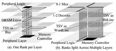
Figure 1 3D-stacked DRAM.
To fully exploit the benefits of 3D stacking technology,another DRAM organization is introduced wherein individual storage-cell arrays are stacked in a 3D fashion.TSVs are used to link these memory arrays from different layer to peripheral logic(e.g.decoder and sense amplifier)in bottom layer[6],as shown in Fig.1 (b).By isolating the peripheral logic implemented with CMOS technology from the DRAM bit-cells implemented with NMOS technology,such architecture not only reduces manufacturing complexity,but also enables individual optimizations of logic layer for speed and storagecell layers for density,thus dramatically reducing memory access time.In addition,TSVs are implemented as part of the bitlines and wordlines,leading to significant increase of memory bandwidth.
Recently,Tezzaron Semiconductor has implemented the above "true" 3D DRAM architecture (see Fig.1 (b)).In their design,one TSV is shared by two wordlines through a 1 to 2 decoder at the edge of each memory array.At another edge of each memory array,8 to 1 multiplexors are placed to control which bitline can connect to the sense amplifier by TSV[15].This design not only reduce the number of TSVs,but also re-lieves the pitch-mismatch problem[15].Even with the above design,such DRAM organization still leads to a massive usage of TSVs with density in the range of tens of thousands of TSV s/mm2,that is,approximately 1.5 million TSVs for 1 Gb memory[10].Consequently,to obtain high manufacturing yield for such 3D DRAM circuits,it is essential to understand the faulty behavior of TSV defects and develop effective test and repair solutions to tolerate such defects.
The primary failure mechanism for TSVs is random open defects (e.g.,caused by void after filling)during TSV fabrication[12].However,we cannot simply model such defects as wordline/bitline stuck-open faults as in[17]for 2D memory circuits.This is because,the extremely high density of TSVs makes ca pacitive coupling effects among them not negligible[11].To tackle this problem,in this paper,we conduct extensive simulations to study the faulty behavior of TSV open defects and map them to functional fault models of the memory circuits,which serves as the first step to tackle the test and repair problem for 3D DRAMs.
The remainder of this paper is organized as follows.Section 2 presents preliminaries of this work.In Section 3,we describe the simulation methodology employed in this work.Next,the simulation results and analysis for wordline opens and bitline opens due to TSV defects are detailed in Sections 4-5.In Section 6,we extend our simulation study by considering the TSV coupling effects from multiple silicon layers in the DRAM.Then,we map the TSV open defect into memory functional fault models and present corresponding test implications in Section 7.Finally,Section 8 concludes this paper.
2 Preliminaries
2.1 Memory Operation
Fig.2 presents an example equivalent circuit with one DRAM layer connecting to the bottom peripheral layer using TSVs.For simplicity,only three wordlines (WL0-WL2) are shown in this figure.With the commonly-used folded bitline DRAM architecture[4],each column in the memory array has two bitlines (BL and BL),intersecting each wordline at two points,wherein one storage-cell is placed in one of these two points.Nevertheless,the storage-cell can be placed in either BL or BL,for example,storage-cells along WL0are all in BL (BLi,BLi+1,...) while those along WL1and WL2are all in BL(BLi,BLi+1,...) (see Fig.2).Pass transistor connects storage-cell with bitline,and it is controlled by the corresponding wordline.

Figure 2 3D DRAM Model.
During write operation,the wordline is driven with logic '1',turning on the pass-transistor.After write enable signal (WE) is turned on,the input data directly drives the bitlines (e.g.,drives BL to '1' and drives BL to '0' simultaneously),charging (discharging) the target cell capacitor.Dur-ing read operation,there are four phases:(i) In precharge phase,both BL and BL are charged as Vrefby precharge circuit.After that,precharge circuit is isolated from bitlines.(ii) In access phase,a specific wordline is accessed by driven to logic '1,turning its pass-transistors on.Then the storage-cell capacitors begin to charge/discharge the BL while BL remains as Vref(i.e.when WL1or WL2is accessed in Fig.2),and vice versa (i.e.when WL0is accessed).(iii) In sensing phase,the minute voltage difference between BL and BL makes the two transistors in diagonal position in sensing circuit more conductive,leading to a positive feedback,which continually enlarges the voltage difference until one of them is pulled up to '1' while the other dragged down to '0'.(iv) Finally,the result comes out through the output circuit and is restored back to the accessed storage-cell.
2.2 Related Work and Motivation
Open defect can be classified as full open defect and resistive open defect.In[17],full open defects in memory circuits are modeled as stuck-open faults.With this fault model,when an open spot occurs on the wordline/bitline,the memory cell becomes unaccessible.Resistive open defects on the wordlines/bitlines of traditional 2D DRAM circuits have also been extensively studied in prior works[27,28]using defect injection and SPICE simulation[3,21].Various address fault models (AFs) have also been proposed to target full open defects in the address decoders[2,22].
Generally speaking,a full open defect breaks an interconnect into two parts:one connected to the source,while the other disconnected as a floating net.According to several electrical models for full interconnect opens[9,14,26],the parasitic capacitances between the floating net and its neighbors may have a significant impact on the voltage of the floating part,and Aggressor-Victim model is commonly used for analysis.For example,in[26],the authors sum up all the coupling capacitance of aggressors having logic value '0/1' as C0/C1.Then it determines the voltage of the floating part by comparing C0and C1.
When TSVs are used as part of the wordlines/bitlines in 3D DRAMs,however,not only they are more prone to random open defects[12],but also their capacitive coupling is more severe when compared to their counterpart in 2D memory,as studied in[11].Previous open fault models hence cannot accurately capture the faulty behavior of TSV open defects in 3D DRAM.In addition,as the coupling effects between aggressor TSVs and victim TSV vary with the operation of the DRAM,the faulty behavior of TSV open defects in 3D DRAM is affected by many factors,e.g.,operation type (i.e.,read or write),voltage of its neighboring word-lines/bitlines and coupling capacitance from its surroundings.Consequently,it is almost impossible to analyze the faulty behavior of such defects statically.The above motivates us to conduct extensive simulations to study TSV open defects.In particular,we focus on full TSV open defects in this work.
3 Simulation Methodology
Based on[6],we set the size of TSV as 1.5 μm×1.5 μm.According to the 3D DRAM cell feature size and the TSV used in wordline/bitline,we estimate the distance between TSVs to be 2~4 μm,considering the TSV sharing mechanism mentioned earlier.The parasitic parameters for TSVs are set according to[11],and two reasonable values 0.6 f F and 1 f F are assumed as the boundary of their coupling capacitance in our simulation,regardless of the TSV open position.The storage-cell intrinsic capacitance is set to be 30 f F .We also set Vdd=1.8 V and reference voltage as half of it.The threshold voltage of each pass-transistor is set to be 0.5 V .Thus,to simulate logic '1' in accessed cells,we set the initial value to be 1.3 V,the maximum voltage can be written into a cell.
In our simulation study,for a victim TSV with an open defect,we only consider the capacitive coupling effects from its neighboring TSVs,because the coupling effects from farther TSVs are usually shielded out by the TSVs in between[11].We are not concerned about the coupling effects between TSVs used to implement part of wordlines and those on bitlines.This is because they are routed outside of two different borders of each DRAM bank respectively,and hence their coupling effects can be ignored.In addition,we differentiate TSVs that are at the border with neighbors at only one side (denoted as border TSVs) and TSVs that are in the middle and hence are surrounded by other TSVs (denoted as middle TSVs),because they suffer from different coupling effects.For the ease of discussion,we denote "Y w X " as write logic X (i.e.,'1' or '0') to a cell with logic Y ('1' or '0').Sim-ilarly,"X r" denotes read from a cell with logic X.We also assume that the coupling effect between TSVs and traditional vias are negligible due to the small size of traditional vias.Since "0w0" and "1w1" operations do not change the cell ca-pacitor,we only consider the following operations:"1w0","0w1","1r",and "0r" in our simulation.
The simulation studies conducted in this work are summarized in Table 1.Simulation for bitline with TSV open defects is rather simple since all the bitlines within a block are accessed in any write or read operation.In other words,BLo and the neighboring bitlines of the BLo are accessed at the same time.For simulation on wordline with TSV open defect,however,we need to differentiate the case for accessing the wordline with open defect and that for accessing the neighbor of the wordline with open defect.In the following,we first show our simulation models and results for wordline/bitline opens considering coupling effects from TSVs originating from the same layer,where there are at most two neighboring aggressors to the floating wire (Section 4~5).Then,in Section 6,we extend the simulation model to consider coupling effects between TSVs passing through different layers.
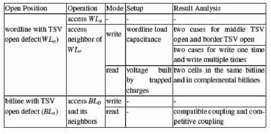
Table 1 Summary of Applied Simulation
4 Simulation for Wordline Opens
4.1 Simulation Setup
For TSV open defect on wordline,the floating part is the wordline in DRAM layer and the pass transistors (MOSFET) on it.According to[14],the gate-to-source voltage (Vgs) of a floating pass transistor depends on three factors:voltage on neighboring nets of the floating wordline (Vmg),the drain-to-source voltage (Vds) that determines the operational region of transistor (i.e.,off,linear or saturation),and the trapped charges deposited during fabrication on the floating gate of pass-transistor[8].As we are not certain about the amount of trapped charges on a particular interconnect open,in this work,we investigate the faulty behavior by varying the voltage built up on floating gate of pass-transistor by trapped charges.
Let us consider the example circuit in Fig.2 and suppose WL1has a TSV open defect,there are two possible cases to be concerned:(i) WL1is accessed(turned on);(ii)one of WL1's neighbors,e.g.,WL2,is accessed.For the former case,as none of its neighbors can be turned on (only one wordline can be accessed in a memory bank),it behaves as a stuck-open fault and we can map it to existing addressed fault models[2,17].We therefore only need to simulate for the latter case (seeTable 1).
Fig.3 (a) shows the schematic circuit used in our simulation for wordline opens.The open defect is represented by a very large resistance Ropen in SPICE simulation.Wordline WL1has an open TSV,and we simply denote it as an wordline with open defect.Wordline WL0(WL2) is the neighboring wordlines.PT0-PT2are the pass transistors.C0and C1are the corresponding coupling capacitance between adjacent TSVs.Cell1is the floating cell while Cell0is the accessed cell when WL0is turned on (Cell2becomes the accessed cell when WL2is turned on).The wire parasitic capacitance in wordline and bitline (Cwand Cb) are not shown in schematic for clarity.We use a voltage pulse source(Vsig) to represent the voltage change.Thus an accessed wordline connects Vsig,while those wordlines turned off connect Gnd.There are two scenarios in terms of the corresponding position between floating cell and accessed cell:(i) the accessed cell (Cell2)and floating cell (Cell1) are in the same bitline;(ii)the accessed cell (Cell0) and floating cell (Cell1) are in the complemental bitlines.We use the following example to demonstrate these two scenarios.

Figure 3 Simulation Model for Write/Read Operation with Wordline Opens.
Fig.3(b) presents the structural view of accessing neighboring wordline of an open one.Let us consider wordline (WL1) is open,thus Cell1is the floating cell.For scenario (i),WL2is accessed and Cell2is the accessed cell.Cell1and Cell2are in the same bitline (BLi).For scenario (ii),WL0is accessed and Cell0is the accessed cell.Cell0and Cell2are in complemental bitlines.
During the write operation there is no difference between these two scenarios,since there is a source driving both BL and BL.Thus,we turn off the sense enable signal SE to isolate the sensing amplifier and drive the bitline BL to corresponding logic (logic '1"or logic '0') (see Fig.3(a)).During read operation,the corresponding position of the accessed cell and floating cell should be considered,because there is no strong source in bitline during sensing phase.Thus,the different corresponding positions of the accessed cell and the floating cell affect the simulation results.As a result,we consider both scenarios when conducting simulations for read operation on wordline with open defect.
4.2 Simulation Results and Analysis for Write Operation
This section presents the result of write operation by accessing neighboring wordline of the wordline with open defect (see Table.1).Both middle TSV with open defect and border TSV with open defect are considered.Furthermore,we conduct simulation studies for both single write operation and multiple write operations.As wordline load capacitance significantly affects simulation results,to further investigate the impact of wordline with TSV open defects,we vary the wordline capacitance from 1 f F to 200 f F in our simulation.
Fig.4 (a)-(b) shows voltage change on Cell1due to the coupling effect between accessed wordline and wordline with open defect when we set the Cwas 10 f F .As can be observed from Fig.4 (a),for middle TSV open,a single "0w1" operation to Cell1can only drive Cell0to 0.4 V due to the weak pulling up capability of NMOS transistor while the "1w0" operation can pull down the voltage of Cell0efficiently.On the other hand,Fig.4 (b) shows the simulation results by apply ing the same operation six time(i.e.,"0w1w1w1w1w1w1"and "1w0w0w0w0w0w0").For wordline with middle TSV open,the voltage can be written into a cell capacitor in "0w1" operation is no more than 0.6 V,while the times needed to write cell capacitor to 0 depends on the coupling capacitance because aggressor TSVs with higher coupling capacitance is more effective to drive the floating cell capacitor.Both Fig.4(a)-(b) show that they are able to drive cell capacitor in a border TSV more aggressively,even with low coupling capacitance 0.6 f F.

Figure 4 Write Operation with Wordline Open when Wordline Load Capacitance is 10 f F
When the load capacitance of wordline is larger than 50 f F,our simulation results show that the voltage change of the wordline with open defect is negligible,forcing the pass-transistor in off mode.As a result,the write operation on neighboring wordline of the wordline with TSV open defect cannot change the voltage of the floating cell.
4.3 Simulation Results and Analysis for Read Operation
This section presents the result of read operation by accessing the neighbor of the wordline with open defect (see Table.1).Both scenarios wherein the floating cell and accessed cell are in the same bitline or in complemental bitlines are considered.Previous results show that a wordline with open defect cannot turn on the pass-transistor when its neighboring wordline are accessed with large load capacitance.However,we cannot simply conclude that the coupling effect between the accessing wordline and the wordline with TSV open defect has no impact on read operation.This is because another important factor of interconnect open,i.e.,trapped charges deposited during fabrication on gate of pass-transistors could build up enough voltage (gate-to-source voltage Vgs) so that the floating cell is accessible[7,18].
Because of this,two storage-cells may be read out at the same time.One is in the accessed wordline (accessed cell) while the other is in the wordline with open defect (floating cell).To investigate the impact of trapped charges on the gate of pass-transistor,we vary the initial voltage (Vtrap) on floating gate of pass-transistor during our simulation.
The simulation study shows that there are two scenarios that the output is affected by a floating cell:(i) when the floating cell and the accessed cell are in the same bitline,and accessed cell is with logic '1' while the floating cell is with logic '0';An example corresponding to this scenario is accessing WL2while Cell1=0 and Cell2=1 in Fig.3(b);(ii) when the floating cell and the accessed cell are in complemental bitlines,and the two cells are both with logic '0'.An example corresponding to this scenario is accessing WL0while Cell0=0 and Cell1=0 in Fig.3 (b).By varying Vtrap,we observe the faulty behavior of scenario (i) when Vtrap≥0.7 V (see Fig.5(a)) and the faulty behavior of case (ii) when Vtrap≥1.0 V (see Fig.5(b)),respectively.Fig.5(a)-(b) present the corresponding results of cells staying in the same bitline and the complemental bitline,respectively.The curves in both figures start at the time when the pass-transistors are turned on (denoted as 'wordline access') and the sense phase (denoted as'SA') starts 5 ns after 'word access' (see Fig.5).In both cases,faulty behavior can be observed when coupling capacitance varies from 0.6 f F to 1 f F .
In Fig.5 (a),Cell1and Cell2are fighting with each other on the same bitline after wordline access.Bitline is first discharged by Cell1,leading to voltage drop.Then,the charging effect from Cell2becomes dominant and pulls up the voltage of bitline.However,it cannot reach Vrefat last,leading to incorrect result.The correct voltage of BLishould be logic '1' but now it is logic '0'.The correct voltage of Cell2should be logic '1' (the voltage in accessed cell remains the same during read operation due to the restore phase),but now it is also logic '0'.The voltage of Cell1remains the same as logic '0'.
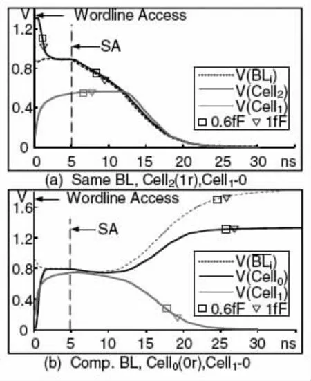
Figure 5 Read Operation with Wordline TSV Open
In Fig.5 (b),Cell0and Cell1are fighting on two complemental bitlines,which are being discharged from Vref(0.9 V).Along with the charging process from bitline to storagecell capacitor,the voltage of storage-cells increases while the voltages in bitline decrease.Thus,Vdsof pass transistor (equal to voltage difference between bitline and cell capacitor) is reduced.The charging process ends when it achieves a balance situation wherein the voltage of cell is approximately equal to the bitline voltage.At this time,however,it is not strong enough to charge the floating cell Cell1from logic '0' to logic '1',because the gate conductivity of floating cell is weaker than that of the accessed cell (Cell0).Thus,during the sense phase (5 ns after wordline access),the voltage in BLiis lower than that in BLi,amplified by sense amplifier,leading to incorrect result.The correct voltage of BLishould be logic '0',but now it is logic '1'.The correct voltage of Cell0should be logic '0',but now it is also logic '1'.The voltage of Cell1remains the same as logic '0'.
5 Simulation for Bitline Opens
5.1 Simulation Setup for Bitline Opens
Fig.6 presents the schematic circuit used in our simulation for bitline BLiwith TSV open defect.The coupling capacitance Ccis between adjacent TSVs.The simulation setup for write operation is less complicated,because sense amplifier is shut down during write operation,and only the storagecells along with accessed wordline are affected.To simulate '0w1',we link a voltage pulse source to the corresponding bitline,and we connect the bitline with the ground to simulate '1w0'.During read operation,all bitlines are floating and at Vrefbetween the end of pre-charge phase and the beginning of sensing phase.We present the simulation results from the sensing phase.All the bitlines are charged/discharged by their storage-cells except the bitline with open TSV defect,and the coupling effect is investigated in our simulation.
5.2 Simulation Results and Analysis for
For write operation on bitline with open TSV defect,we find that the voltage change in storage-cell in the bitline with open defect is negligible,by driving logic '1' or logic '0' respectively to all bitilnes.If the initial voltage of the accessed cell in open bitline is logic '0',no matter what logic is written into these bitlines,the voltage of storage-cell remains near to 0 V.If the initial voltage of the accessed cell in open bitline is logic '1',no matter what logic is written into these bitlines,the voltage of storage-cell is reduced dramatically.This is because,comparing to the large parasitic capacitance in the bitline,the coupling effect from neighboring bitlines is negligible.In addition,the sense amplifier is shut down during write operation.As a result,the voltage drop in accessed cell is caused by discharging from accessed cell to parasitic capacitance of the open bitline.In practice,both write operations on open bitline and its neighbors do not change the behavior of the open bitline.

Figure 6 Simulation Model for Write/Read Operation with Bitline Opens
5.3 Simulation Results and Analysis for
Suppose bitline BLisuffers from TSV open defect in an example circuit shown in Fig.7.For read operation with BLi,let us consider two cases:(i) If we access WL0,bitline BLiis driven by Cell3.Although bitline BLiis floating with reference voltage due to open defect,the sense amplifier can still sense the voltage difference between BLiand BLiand then drive both bitlines to opposite voltages.In this case,the open defect does not influence the output of read operation.(ii) If we access WL1,bitline BLiis floating because there is no storage-cell being accessed in BLi.At the same time,bitline BLiis also floating due to the TSV open defect.Thus,bitline BLiis indirectly influenced by Cell1on bitline BLi-1via the neighboring bitline BLi-1while bitline BLiis directly influenced by Cell7on bitline BLi+1(see the arrows in Fig.7).As a result,we run simulation for the latter case to see the corresponding faulty behavior.
We conduct two simulations for read operation with BLiopen.Fig.8 (a) presents the results when the neighbors BLi-1and BLi+1drive BLiand BLiwith opposite logic values (one is logic '1' while the other is logic '0').The logic value of BLiremains the same with varying coupling capacitance.This isbecause the voltage difference between BLi and BLiis amplified by the sensing circuit,charging BLiand BLito opposite logic values.The output of the open bitline is reinforced by both of its neighboring bitlines.We denote this faulty behavior as compatible coupling fault.

Figure 7 Read with Bitline Open:An Example
Fig.8 (b) presents the results when two neighbors,BLi-1and BLi+1drive BLiand BLiwith the same logic value (both '1' or both '0').Simulation results show that the logic value of open bitline BLiis determined by Cell7,since Cell7is coupled with BLi,the complemental bitline of BLi.We denote the driving force as the capability to drive the open bitline through capacitive coupling.The larger distance between the aggressor bitline (TSVs) and the open bitline (TSV) is,the smaller coupling capacitance is.Since BLi-1and BLi+1have the same storage-cell value during the read operation,they pull up (or pull down) BLiand BLiat the same time.The coupling capacitance from BLi+1to BLiis larger than that from BLi-1to BLi,and hence the driving force of BLi+1is larger,making BLi+1dominate the logic value in BLi.We denote this faulty behavior as a competitive coupling fault.
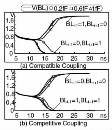
Figure 8 Compatible and Competitive Coupling in Read Operation with BLi Open
Similar results are obtained with varying coupling capacitance Cc.The reason is that,the sense amplifiers are active during sensing phase of read operation.Even if the coupling capacitance is small (e.g.,0.2 f F) between neighboring bitlines,the small voltage changes in open bitline generated by this coupling capacitance can be amplified by the sensing circuit.
6 TSV Coupling Effects from Multiple Layers
In this section,we consider capacitive coupling from aggressor TSVs on multiple layers.Using Aggressor-Victim Model[26],we can extend our earlier simulation model for such additional TSV coupling effects.
For wordline open simulation,based on the capacitance extraction model presented in[19],we first calculate the sum of capacitance coupled to all possible neighboring TSVs driven by logic '1' and '0',respectively.Then,we change the value of coupling capacitance parameters (e.g.C1is the sum of those capacitances coupling to wordlines driven by logic '1'and C0is the sum of those capacitance coupling to wordline driven by logic '0') with the calculated values and conduct simulation using the same schematic circuit in Fig.9.
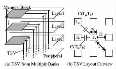
Figure 9 TSV Coupling from Multiple Layers
Fig.10 shows two cases in terms of different wordline ac-cess address.'i' denotes the TSV with open defect while '1' denotes the neighboring TSVs of wordline being accessed.In Fig.10 (a),the three banks are within the same memory rank so that the wordlines with the same local address within the bank are accessed simultaneously.In many DRAMs,the bank within the same rank can operate independently.Based on this,Fig.10 (b) shows an extreme case wherein the coupling capacitance from neighboring wordline is maximized.For both cases,the faulty behaviors of write/read operation are similar to previous simulation results (in Fig.4 and Fig.5).
For bitline open simulation,the faulty behavior of bitline opens are quite similar to what we have studied in Section 5.We only need to know the driving forces among all the neighbors of the open bitline.If the driving force for logic '1' is larger than that for logic '0',the open bitline read as logic '1',otherwise logic '0'.
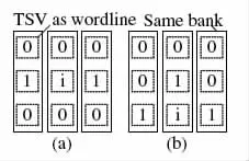
Figure 10 Considering TSV Coupling from Multiple Layers for Wordline Open
7 Fault Modeling and Test Implications
In this section,we map the TSV open defect into mem-ory functional fault models according to our simulation.The fault models caused by TSV open defect in wordline/bitline are summarized in Table 2.It should be noted that,the no ac-cess behavior has been studied in previous works,modeled as stuck-open fault and we can map it into one kind of memory address fault,AFna[2].

Table 2 Summary of Fault Models
7.1 Wordline Open
When we access the wordline with TSV open defects,we cannot access the corresponding cells,denoted as No Access Behavior.Consequently,write operation cannot change the values in the storage-cell,and read operation cannot change the voltage of bitline,leaving the bitlines in reference voltage.While this can be mapped into the AFna memory address fault in traditional 2D memory circuits,the difference is that,all cells within this wordline are unable to access,and all the bitlines within this block stay in reference voltage.Hence,any capacitive coupling from neighboring blocks or neighboring layers could impact the bitline voltages,leading to different faulty behavior under different 3D memory design.
When we access the storage-cell on the neighboring wordline of the wordline with open defect,the floating cell on this wordline is accessed too,depending on the wordline load capacitance and trapped charges within the gate of pass-transistor deposited during fabrication.This faulty behavior is defined as Multiple Access Behavior.For write operation,the floating cell cannot be modified with relatively large load capacitance.For read operation,the logic value in bitline (BL) and the content in accessed cell (Cell1) are both incorrect (Fig.5(a)-(b)),denoted as a Read Disturb Faults (RDF)[27].
7.2 Bitline Open
The write operation with bitline opens has negligible impact on its accessed cell,denoted as No Access Behavior.In this work,we only model the fault of read operation with bitline opens.As discussed in Section 5.3,there are two types of coupling faults caused by bitline with open TSV,denoted as compatible coupling faults and competitive coupling faults,respectively.Suppose BLiis open and given the logic values in BLi-1and BLi+1,Table 3 presents the logic value of BLicaused by capacitive coupling.Once a wordline is selected,all storage-cells in this wordline are accessed.These accessed cells might be in two positions:bitlines (BL1,BL2,...,BLi) or complemental bitlines (BL1,BL2,...,BLi).As mentioned in Section 5.3,compatible coupling faults are sensitized when two neighbors of the bitline with open defect (BLi) have opposite logic values while competitive coupling faults are sensitized when these two neighbors have the same logic values (see Column 2 and Column 4 for compatible coupling and Column 6 and Column 8 for competitive coupling).Let us take the first row in compatible coupling faults (see Table 3) as an example.When WL1in Fig.7 is selected,Cell1and Cell7are accessed,driving BLi-1and BLi+1to logic '1' and logic '0',respectively.Then,BLi-1drives BLito logic'1' and BLi+1drives BLito logic '0'.The output of BLiis hence logic '1'.
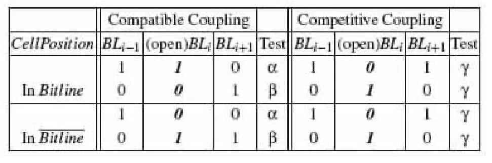
Table 3 Fault Modeling for Read Operation with Bitline Open
The faulty behavior in read operation with bitline open defect can be mapped to the well-known neighborhood pattern sensitive fault (NPSF).We develop the following tests to cover all the faulty behavior shown in Table 3:

7.3 Wordline/Bitline TSV Open with Multi-Layer Coupling
The crossing bank effect of capacitive coupling changes the normal memory test algorithms dramatically.That is because,in 2D memory,the test in different memory bank are independent,making it possible to test the memory chip in a highly parallel manner.However,in 3D memory,we have to write test patterns to memory cells in multiple banks to satisfy the test condition.
8 Conclusion and Future Work
The large number of TSVs implemented in 3D-stacked DRAM circuits are prone to open defects and coupling noises,leading to new test challenges.In this paper,we model the faulty behaviors of such defects with extensive simulation studies,map theminto memory functional fault models,and present the corresponding test implications.
In our future work,we plan to study test algorithms and the associated BIST structure to detect TSV open defects.In addition,this work focuses on TSVs with full open defects.As TSVs can also be resistive open[27]and may exhibit different faulty behavior,we plan to also consider resistive open defect on wordline/bitline in our future work.
9 Acknowledgements
This work was supported in part by the General Re-search Fund CUHK417807 and CUHK418708 from Hong Kong SAR Research Grants Council(RGC),in part by Na-tional Science Foundation of China (NSFC) under grant No.60876029,and in part by a grant N CUHK417/08 from the NSFC/RGC Joint Research Scheme.
[1]A.V.Goor and C.Verruijt.An Overview of Determin istic Functional RAM Chip Testing[J].ACM Computing Surveys,22(1):5-33,1990.
[2]A.J.van de Goor.Testing Semiconductor Memories:Theory and Practice[M].ComTex Publishing,1998.
[3]A.J.van de Goor and A.Paalvast.Industrial Evalua tion of DRAM SIMMTests[J].Proc.International Test Conference (ITC).,pp.426-435,2000.
[4]B.Jacob,S.Ng,D.Wang.Memory Systems:Cache,DRAM,Disk[M].Morgan Kaufmann,2007.
[5]C.Liu,et al.Bridging the Processor-memory Perfor mance Gap with 3D IC Technology[J].IEEE Design&Test of Computers,22(6):556-564,2005.
[6]G.Loh.3D-Stacked Memory Architectures for Mul ti-core Processors.In Proc[C].International Symposium on Computer Architecture (ISCA),pp.453-464,2008.
[7]H.Konuk,F.J.Ferguson.An Unexpected Factor in Testing for CMOS Opens:The Die Surface.Proc[C].VLSI Test Symposium (VTS),pp.422-429,1996.
[8]H.Konuk.Voltage-and Current-based Fault Simulation for Intercon-nect Open Defects[J].IEEE Transactions on Computer-Aided Design of Integrated Circuits and Systems.,18(1):12,1999.
[9]H.Konuk.Voltage-and Current-based Fault Simulation for Intercon-nect Open Defects[J].IEEE Transactions on Computer-Aided Design of Integrated Circuits and Systems,18(12):1768-1779,1999.
[10]H.Sangki.3D Super-Via for Memory Applications[M].In Micro-Systems Packaging Initiative Packaging Workshop (MSPI).,2007.
[11]I.Savidis and E.Friedman.Electrical Modeling and Characterization of 3-D Vias.In Proc[J].IEEE Interna tional Symposium on Circuits and Systems (ISCAS),pp.784-787,2008.
[12]I.Loi,et al.A Low-overhead Fault Tolerance Scheme for TSV-based 3D Network on Chip Links.In Proc[C].IEEE/ACM International Con-ference on Comput er-Aided Design (ICCAD),pp.598-602,2008.
[13]International Technology Roadmap for Semiconductors(ITRS)[EB/OL].2009.www.itrs.net,2009.
[14]M.Renovell and G.Cambon.Electrical Analysis and Modeling of Floating-gate Fault[J].IEEE Transactions on Computer-Aided Design of Integrated Circuits and Systems,11(11):1450-1458,1992.
[15]M.F.Hilbert.High-Density Memory Utilizing Multi plexers to Reduce Bitline Pitch Constraints[Z].US Patent 6,377,504,2002.
[16]M.Kawano,et al.A 3D Packaging Technology for 4 Gbit Stacked DRAM with 3 Gbps Data Transfer.In Proc[C].International Electron Devices Meeting,pp.1-4,2006.
[17]R.Dekker,F.Beenker,and L.Thijssen.Fault Model ing and Test Al-gorithm Development for Static Ran dom Access Memories.In Proc[C].International Test Conference (ITC),pp.343-352,1988.
[18]S.Johnson.Residual Charge on the Faulty Floating Gate CMOS Tran-sistor.Proc[C].International Test Conference (ITC).,pp.555-561,1994.
[19]S.Wong,G.Lee,and D.Ma.Modeling of Intercon nect Capacitance,Delay,and Crosstalk in VLSI[J].IEEE Transactions on semiconductor manufacturing,13(1):108-111,2000.
[20]S.Gupta,et al.Techniques for Producing 3D ICs with High-density Interconnect[M].In Proc.International VLSI Multilevel Interconnection Conference,2004.
[21]S.Hamdioui,G.Gaydadjiev and A.J.van de Goor.The State-of-Art and Future Trends in Testing Em bedded Memories[J].Proc.IEEE International Work shop on Memory Technology,Design and Testing.,pp.59,2004.
[22]S.Hamdioui,Z.Al-Ars,and A.J.van de Goor.Opens and Delay Faults in CMOS RAM Address De coders[J].IEEE Transactions on Comput-ers.,pp.1630-1639,2006.
[23]Tezzaron Semiconductors.Leo FaStack 1Gb DDR SDRAM Datasheet[M].,August 2002.
[24]U.Kang et al.8Gb 3D DDR3 Dram Using Through-Silicon-Via Technology[J].In Proc.Interna tional Solid State Circuits Conference (ISSCC),pp.130-131,2009.
[25]W.R.Davis,et al.Demystifying 3D ICs:The Pros and Cons of Going Vertical[J].IEEE Design&Test of Computers,22(6):498-510,2005.
[26]Y.Sato,et al.A Persistent Diagnostic Technique for Unstable Defects[C].In Proc.International Test Confer ence (ITC),pp.242-249,2002.
