Design of a novel correlative reflection electron microscope for in-situ real-time chemical analysis∗
2021-12-22TianLongLi李天龙ZhengWei魏征andWeiShiWan万唯实
Tian-Long Li(李天龙) Zheng Wei(魏征) and Wei-Shi Wan(万唯实)
1School of Physical Science and Technology,Shanghai Tech University,Shanghai 201210,China
2College of Materials Science and Engineering,Chongqing University,Chongqing 401331,China
Keywords: reflection high energy electron diffraction (RHEED), electron energy loss spectroscopy (EELS),parallel detection,energy-filtered electron microscopy
1. Introduction
Reflection high-energy electron diffraction (RHEED) is a powerful laboratory-basedin-situtool to monitor the extremely small changes at surfaces in the epitaxial growth process with sub-monolayer sensitivity. Most of RHEED setups record the diffraction patterns of all scattered high-energy electrons striking at surfaces with a small glancing incident angle in a range of 0◦–10◦, without distinguishing the elastically scattered electrons from the inelastically scattered electrons. In order to quantitatively determine the atomic structures of the surfaces, it is crucial to remove the inelastically multiple scattered electron features,such as the Kikuchi lines and the broadening of Bragg spot profiles. These high-pass energy-filtered RHEED setups have been realized by several groups.[1–4]In order to perform the chemical analysis of the surfaces,the RHEED setup can be combined with either total reflection angle x-ray spectroscopy(TRAXS),[5]or reflection electron energy loss spectroscopy(REELS),[6]thus possessing a very low spatial resolution in a range of 1 mm–10 mm determined by the illuminating size of the incident electron beam on the surface. However,there are few reports that attempt to quantitatively investigate the superstructures and to perform the chemical analysis of surface atoms simultaneously.
In this work, we propose an electron optics design for a novel correlative reflection electron microscope(c-REM)with three modes of diffraction,spectroscopy,and imaging working simultaneously. Our simulation demonstrates that this c-REM can simultaneously record the RHEED pattern,the energy loss spectra of inelastically scattered electron,and the REM image of the elastically scattered electrons with a spatial resolution of 50 nm.
2. Methods
The electron optical system is designed and simulated using the simulation code COSY INFINITY.[7]Of the various numerical simulation codes developed for the field of electron optics, COSY INFINITY, which is based on differential algebra (DA),[8]is the fastest and the most powerful. Unlike the traditional raytracing method, differential algebraic technique obtains the transfer map of an arbitrary order through integrating numerically the equations of motion, thus obtaining all aberrations up to a given order at once. As a result,the tracking of the electrons through the optical system can be carried out using the transfer map,making it orders of magnitude faster than the ray tracing method. For example,tracking 104electrons by using a fifth-order map on a PC takes less than a minute.
The fringe field distribution of the bending magnet(BM)is modeled using the Schwartz–Christoffel model.[9,10]The field distribution of the magnetic round lenses is calculated based on the Gray model,[11]

whereB0is the field ats=0,lis half of the distance between the magnetic poles, anddis the radius of the poles. Here we setl=d=6 mm.
3. Electron optics
The electron optics of the c-REM is sequentially attached to the back of a RHEED detector I as schematically shown in Fig. 1. The scattered electrons along a specific diffraction direction can be steered to pass through a small hole in the RHEED detector I, and energy is dispersed by a 90◦bending magnet (BM) downstream. Inelastic electrons, which are energy dispersed by the BM, strike on the EELS detector II,while elastic electrons pass through the slit along theydirection. Afterwards,these elastic electrons will be magnified and projected by two magnetic round lenses and eventually hit the REM detector III. The distance for the main components of the c-REM with respect to the illuminated point on the sample are listed in the inset table.
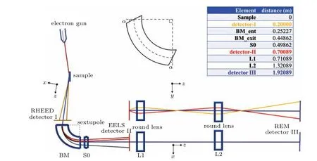
Fig.1. Schematic diagram of main components of c-REM with their corresponding distance to the illuminating point of the sample as indicated in the inset table.Inset shows detailed diagram of bending magnet,with α=26.9◦.Since the radius of the edge is large(610 mm)in comparison with bending radius of magnet(125 mm),the curvature is not apparent to eyes.
In order to minimize the second order geometric aberrations, we shape the entrance edge and exit edge of the magnet into arcs with the same radius of curvature as indicated in the inset of Fig. 1. The value of the edge angle (26.9◦for both edges) is chosen such that a stigmatic image is formed and the remained aberrations are greatly reduced due to mirror symmetry. The remaining second-order aberration along the energy dispersion direction (x|aδ), which causes the image plane to tilt, can be further corrected by a sextupole magnet(S0). For a 5-cm-long sextupole placed 5-cm downstream of the BM,the required sextupole strength is−0.49 T/m2.
The magnification of the EELS image on detector II of the BM is−1 and the magnification of the REM image on detector III is−2970.The two magnetic round lenses are identical with the same excitation currents. The magnetic fields are set to be opposite to each other between L1 and L2,which avoids rotating the image on the REM detector III.This is for conveniently interpreting the features in the REM image,especially during the alignment and optimization procedures of the instrument.
4. Results
In order to evaluate the energy-and spatial-resolution of the c-REM, we perform a series of ray tracing calculations.First,the 5th order transfer map of the setup is generated. Second, the initial phase space coordinates of a set of 104electrons are generated using a random number generator with Gaussian distribution. Third, the set of electrons is plugged into the transfer map and the final coordinates are obtained.All these simulations are carried out using COSY INFINITY,while the data are analyzed and presented with the packages of MATLAB.[12]
Figure 2(a) shows a simulated diffraction spot passing through the RHEED detector I, which corresponds to an rms cone angle of 0.2 mrad with respect to the primary electron beam direction:px,y/p0. Since the distance between the RHEED detector I and the illuminating spot on the sample is 200 mm, the projected pattern has an FWHM diameter of 80µm,corresponding to the typical smallest aperture size used in an electron microscope as shown in Fig.2(b).
To determine the energy resolution of this instrument,Rayleigh criterion is employed,in which only the electron energy difference is tuned, while other parameter such as the angle divergence is fixed at 0.2 mrad, the same asyhat in Fig.2. The simulated one-dimensional energy dispersion pattern on the image plane of EELS detector II is shown in Fig.3,with four relative energy differences of 1×10⁻⁴, 3×10−5,2.5×10−5, and 1.5×10⁻⁵, with respect to the primary electron energyE0. It is determined that the relative energy resolution of the system is around 2.5×10⁻⁵.
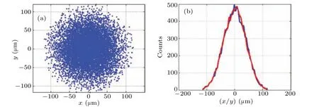
Fig.2. Simulated diffraction spot passing through hole of RHEED detector I,showing(a)two-dimensional projections of initial distributions of electron,and(b)profile along x=0(blue)and y=0(red).

Fig. 3. Dispersion of electrons on EELS detector II, with electron energy difference of (a) 1×10⁻⁴, (b) 3×10⁻⁵, (c) 2.5×10⁻⁵, and (d)1.5×10⁻⁵ with respect to the primary electron energy E0.

Fig.4. Projected distribution of electrons(a)along x direction on EELS detector-II(red)and REM detector III(blue,scaled by 1/2970),and(b)along non-dispersive y-direction for electron with energy differences δ =2.5×10⁻⁵(red)and 0(blue)on EELS detector-II.
For the 15-keV electrons, the absolute energy resolution is 0.375 eV,which corresponds to the typical energy spread of electrons emitted from cold field-emitters. At EELS detector II,the energy resolution is limited mainly by the pixel size of the detector. Assuming that 3 pixels are required to resolve a peak with a pixel size of 30 µm, the absolute energy resolution is roughly 5.4 eV,which is comparable to the counterpart of the EELS on the market.[6]To achieve the best resolution of this instrument,a magnified image of the energy spectrum can be formed on REM detector III where only a fraction of the full spectrum can be displayed. Furthermore, figure 4 shows that the projector lenses L1 and L2 behind the BM do not affect the energy resolution,i.e.,the aberrations of those lenses are negligible. In consequence, they hardly contribute to the spatial resolution of the REM images as shown in the following Fig.5.
To evaluate the spatial resolution of the c-REM system,we let the sample with a 5×5 grid arrays in square emit electrons, each grid point with 104electrons. Three sets of grid arrays are simulated,with different spot spacing values of 2.5,7.5,and 25µm,respectively.
For electrons with an rms angular spread of 0.2 mrad,their projections on the REM detector III are presented in Fig. 5. It is worth noting that the spot spacing is magnified 2970 times behind two projection lenses,while the square features of the grid arrays are kept quite well in the field of view of 50µm×50µm.
Marginal distortions from the square are observable only for the largest field of view of 100µm×100µm,for the corner spots(Nos.1,5,21,and 25)as shown in Fig.5(c).More quantitative results for Fig.5(c)are listed in Table 1. The fact that the resolution at spot Nos.21 and 25 are much worse than at Nos.1 and 5 indicates that the second-order aberrations from the bending magnet play an important role in large off-axis distance of 100 µm. Through tuning the curvaturehof both the entrance and exit edges of the BM, as shown in the inset of Fig. 1, the spatial resolution in theydirection can be significantly improved. Specifically,the second-order geometric aberrations in theydirection are largely suppressed as shown in Table 1,forh=−1.64 and spot distance of 25µm.The spatial resolutions achievable at the edge of a large field view of 100µm×100µm are improved from 98 nm–137 nm to 59 nm–93 nm as shown in Table 1,and reach the limit of 35 nm–52 nm in the distortion-free center region of 30µm×30µm as indicated in Table 2.
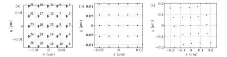
Fig.5. Final distributions of electrons arriving on the REM detector-III with electronsemitted from a 5×5 grid with ∆x =∆y =2.5, 7.5, and 25µm,respectively.
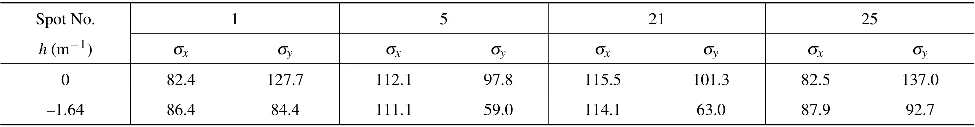
Table 1. Comparison among spatial resolutions of REM images at four spots on sample in Fig.5(c),with different curvatures at the edge of field view of 100µm×100µm(unit: nm).
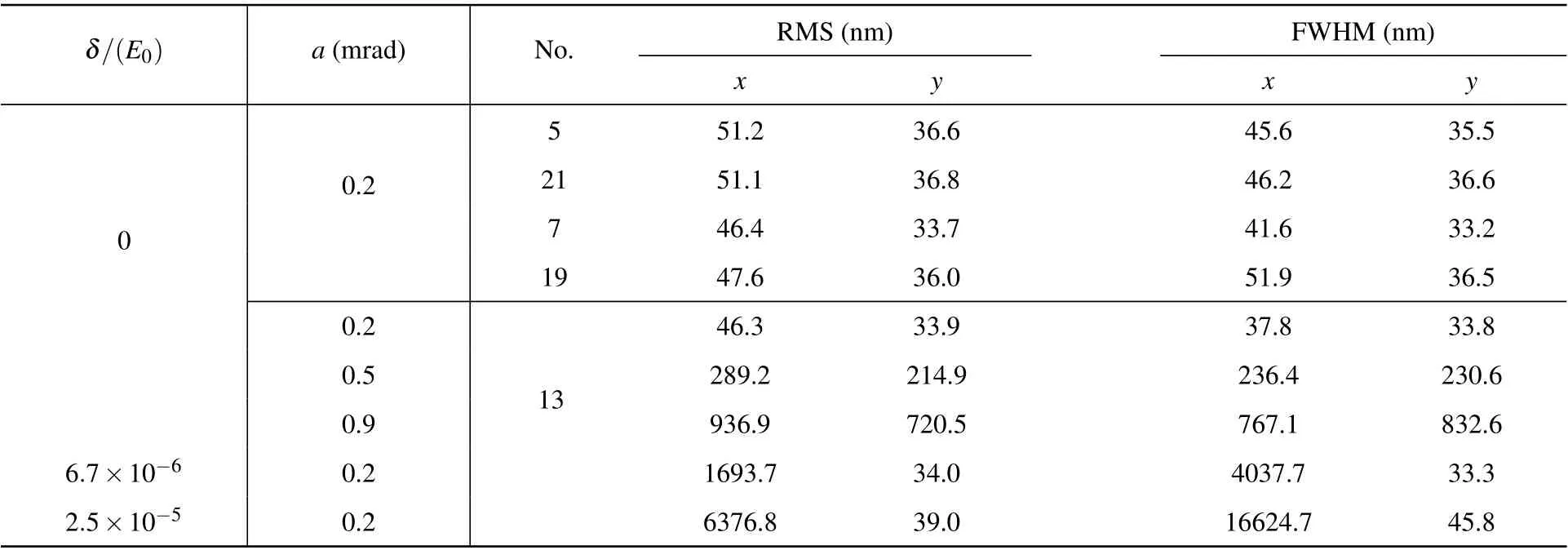
Table 2. Spatial resolutions of REM images corresponding to the typical spots in Fig. 5(b) with field of view 30 µm×30 µm, for different initial parameters such as emission angle dispersion a and energy difference δ.
Table 2 also demonstrates that the spatial resolutions of the REM image are strongly dependent on the dispersions of both emission angle and energy of the elastically scattered electrons. For electrons with larger angular dispersion of 0.5 mrad and 0.9 mrad in FWHM, the spatial resolutions quickly increase from∼40 nm to∼900 nm in bothxandydirections. The energy dispersion of 100 meV and 375 meV(6.7×10⁻⁶and 2.5×10⁻⁵inE0)further spoil the spatial resolution to above 1.7µm inxdirection,while the spatial resolution along the non-dispersionydirection can be preserved to below 50 nm.
5. Conclusions
In this work,the c-REM presented in this paper allows us to detect the diffraction pattern,the energy spectrum as well as real space image of the same surface region at the same time.The spatial resolution of the non-dispersive direction can reach 50 nm in the typical working conditions of RHEED setup,providing new capabilities for the experimentalists.
猜你喜欢
杂志排行

Chinese Physics B的其它文章
- Transient transition behaviors of fractional-order simplest chaotic circuit with bi-stable locally-active memristor and its ARM-based implementation
- Modeling and dynamics of double Hindmarsh–Rose neuron with memristor-based magnetic coupling and time delay∗
- Cascade discrete memristive maps for enhancing chaos∗
- A review on the design of ternary logic circuits∗
- Extended phase diagram of La1−xCaxMnO3 by interfacial engineering∗
- A double quantum dot defined by top gates in a single crystalline InSb nanosheet∗