A review on the design of ternary logic circuits∗
2021-12-22XiaoYuanWang王晓媛ChuanTaoDong董传涛ZhiRuWu吴志茹andZhiQunCheng程知群
Xiao-Yuan Wang(王晓媛), Chuan-Tao Dong(董传涛), Zhi-Ru Wu(吴志茹), and Zhi-Qun Cheng(程知群)
School of Electronics and Information,Hangzhou Dianzi University,Hangzhou 310018,China
Keywords: ternary logic circuit,memristor,digital logic circuit,circuit design
1. Introduction
With the rapid development of modern information technology and improved integration of digital systems, the limit of interconnection has become prominent in realizing binary logic in nano-scale circuit design. The interconnection lines used in integrated circuit design increase the delay,noise,and power consumption of the system, so circuit interconnection has become one of the essential indicators to judge the performance of integrated circuit systems.[1]
There are only two logic states of‘0’and‘1’in traditional binary logic.Multi-valued logic is extended from binary logic,referring to the logic that the number of the logic values is greater than 2. For a multi-value system,when the base value ise,the complexity and cost of the whole system are the lowest,and 3,as the integer closest toe,becomes the best choice.As a kind of multi-valued logic,ternary logic has higher logic complexity. For example,forN-bit digital logic,the complexity of the ternary digital logic is 3N/2Ntimes that of the binary logic. Therefore, the ternary digital logic system has more logic functions. In terms of data representation ability,ternary requires about 58.5% fewer bits than binary to represent the same value, which reduces the complexity of data management, especially when dealing with a large number of issues such as data encryption. The interconnection complexity of the system will also be reduced to realize the corresponding logic function because ternary logic has a higher single-line information-carrying capacity,and the digital chip can also be smaller and lower in cost. For the A/D and D/A conversion accuracy of ternary digital logic circuits,the value represented by the ternary logic is larger than the value represented by the binary logic in the case of the same number of bits,so the A/D and D/A conversion accuracy is much higher. In addition,the ternary digital logic system can be backward compatible with the binary logic system, and there are corresponding expansions in function. In this way, multi-valued logic becomes a promising substitute for binary logic to realize high-density information logic system.[2–5]
The research of ternary logic can be roughly divided into three aspects: mathematical theory, ternary logic devices and basic logic circuits,and the applied research on ternary logic.The theoretical study of ternary logic contains various theorems and logical systems, providing the theoretical basis for the latter two pieces of research. We will introduce the basic ternary theoretical knowledge in Section 2. The second part is the critical content of this article. A corresponding summary of the research findings in this field can provide certain guidelines for the further development of the ternary digital system, such as further improving the data density and logic functions of the digital system. The related application of ternary logic began in 1840 when the British inventor Thomas Fowler first proposed a ternary logic system.[6]Then in 1960, the world’s first small ternary computer ‘SETUN’appeared at Moscow University in the Soviet Union.[7]In 1973, the State University of New York implemented a ternary computer‘TERNEC’through program simulation on a B1700 type microcomputer,[8]using two binary bits to encode each ternary digit to simulate ternary arithmetic operations. In 1984,the Queen’s University laboratory in Canada developed the CMOS ternary computer QTC-1.[9]However, due to the lack of support for ternary logic devices in the semiconductor industry, ternary computers have not been widely developed and further applied.[10]
In recent years,the continuous emergence of various electronic devices has provided new options to realize ternary circuits, such as MOSFETs, carbon nanotube field effect tubes(CNTFETs),memristors,etc.[11–13]In particular,the successful development of memristor has provided more possibilities for the design of ternary logic circuits. The characteristics of non-volatility, nanometer size and compatibility with CMOS technology of memristor have great potential in ternary logic circuits design. Compared with circuits designed using transistors, the circuit structure is simpler and more conducive to integration. Therefore, summarizing the relevant research results of the ternary logic circuit design at this time can provide a reference for the subsequent theoretical and application research of multi-valued logic.
The rest of this paper is composed as follows: Section 2 briefly introduces the three numerical representation methods of ternary logic,and Section 3 shows several mainstream process methods for constructing ternary basic logic gates in detail, several general design methods of ternary combinational logic application circuits are described in Section 4,Section 5 summarizes the ternary sequential logic circuits, and finally,Section 6 concluded this article.
2. Ternary numeric representation
As we all know,binary logic only uses‘0’and‘1’to represent logical states,and has been widely used,so why do we need to study ternary digital logic? One important reason is that ternary digital logic is another means and effective method to solve some practical problems. For example,in the field of digital control, ternary logic can indicate the ‘on’, ‘off’ and‘idle’of an equipment.
The representation methods of ternary logic consist of two categories: unbalanced and balanced. Among them,the unbalanced include positive ternary{0,1,2}and negative ternary{0,−1,−2}, which are relative in the direction of the logical sign. The balanced ternary is represented by{−1,0,1}.[14]In this article, we will focus on the design of unbalanced ternary logic circuits.
2.1. Unbalanced ternary
Due to the relativity of the positive ternary and negative ternary logic states, the two are similar in terms of technical solutions,and the difference lies in the carry direction. Based on the fact that the research of negative logic circuits is rare in asymmetric ternary logic, only the relevant numerical representations of positive ternary logic are described here on account of practical application.
The basic operations of positive three-valued logic can be defined as[15]


whereXi,Xj={0,1,2},‘+’and‘·’respectively represent the‘OR’operation and‘AND’operation of positive ternary logic,and the third formula is ‘NOT’ operation. It is worth noting that the ‘NOT’ operation (inverter) of ternary logic has three forms,and the mathematical expressions are respectively

wherexis the input,y0,y1,andy2are the outputs of the three inverters, corresponding to NTI (negative ternary inverter),STI (standard ternary inverter), and PTI (positive ternary inverter),respectively.
2.2. Balanced ternary
In fact, ak-bit balanced ternary integerx=(xk−1xk−2...x1x0)3represents the value ∑0≤i≤k−1xi3i,wherexi ∈{−1,0,1}. Due to the symmetry of the balanced ternary symbol, the range of numbers that thek-bit balanced ternary integer represents is also symmetric, from−(3k −1)/2 to(3k −1)/2. As a result, the advantage of balanced ternary to represent the entire integer range without the sign bit is significant. In addition,for any integer represented by the balanced ternary,the opposite of the integer number can be obtained by replacing‘−1’of each bit of the integer with‘1’and‘1’with‘−1’.[16]
In addition,the balanced ternary multiplication operation does not generate a carry. Under the condition that all the nine kinds of addition operation input, only two types have a carry generation,[10]as shown in Fig. 1. Therefore, balanced ternary logic has certain advantages over unbalanced types in arithmetic operations.
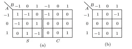
Fig.1. Karnaugh map of balanced ternary(a)half adder and(b)multiplier.
3. General technical solution for the design of ternary logic gates
In binary logic, AND, OR, and NOT can form a complete set of operations. Ternary logic can first construct a series of basic logic gates,and then combinational logic circuits designed can achieve more complex functions. Of course,some unique methods can also directly design ternary application type combinational logic circuits without using basic logic gates.[17,18]
According to the ternary numerical representation discussed in Section 2, the truth tables of positive ternary AND gate and OR gate can be obtained as shown in Table 1. Similarly, Table 2 shows the truth tables of the three inverters.This section will give a detailed description of several typical processes for the design of ternary logic basic gates, including MOSFET, CNTFET, memristive hybrid (voltage value as a logic variable), and memristor (resistance value state as a logic variable). Furthermore,the ternary basic gates designed by other technologies are also summarized.
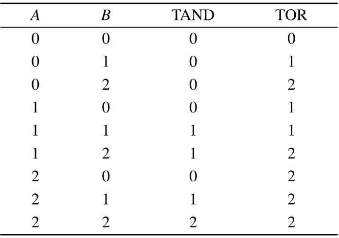
Table 1. Truth table of TAND and TOR.
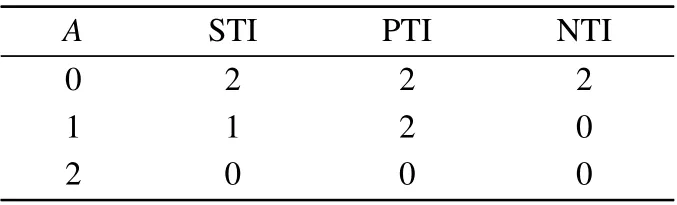
Table 2. Truth table of ternary inverter.
3.1. Design of ternary logic gates based on MOSFETs
In the early MOSFETs-based ternary basic gates design,the complementary structure of P-channel and N-channel transistors was used in a symmetrical way to obtain three different logic levels.[19,20]At the same time,the power supply was much higher than the threshold voltage of the transistor,leading to high circuit complexity and power consumption. In response to this problem, in 1980, reference [21] proposed a novel design method as shown in Figs. 2–4. The PTI, NTI,positive and negative TNAND, TNOR adopted by the asymmetrical structure greatly reduced the complexity and cost of the circuit.
The necessary usage of resistors for ternary circuits mentioned above can generate a certain amount of static power consumption. For this reason,references[22,23]have successively proposed two ternary basic logic gate design schemes that do not require resistors and only use four types of MOS transistors, thereby reducing the static power consumption of the circuit and reducing the number of components used.It also reduces the propagation delay at the same time. In Ref.[22],STI only requires four transistors,NTI and PTI require two transistors. The structures of NTI and PTI are the same.The difference is the threshold voltage of the MOS transistors. Combining the TNOR and TNAND gates designed in the article, a complete set of ternary logic circuit families is constructed, and the design of decoders and shift registers is further realized. Compared with Ref. [22], the circuits designed in Ref.[23]are more complicated,but the paper gives a ternary full adder design based on the improved logic gates.
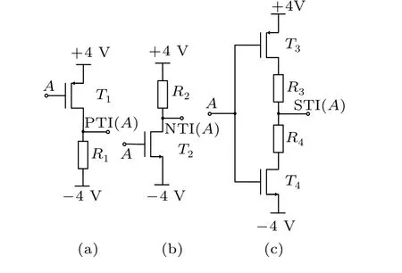
Fig.2. (a)PTI,(b)NTI and(c)STI in Ref.[21].
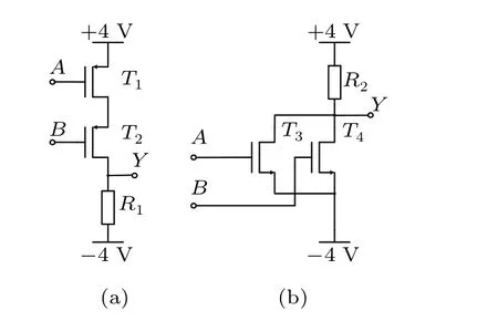
Fig.3. (a)PTNOR and(b)NTNOR in Ref.[21].
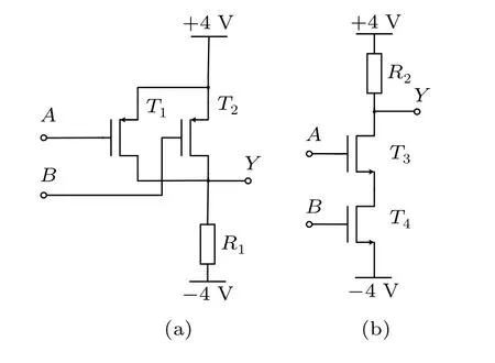
Fig.4. (a)PTNAND and(b)NTNAND in Ref.[21].
To get the complexity and power consumption of the ternary basic gates designed based on MOSFET further reduced, reference [24] proposed a design method that only a single power supply exists,which not only reduced the overall power consumption of the circuit but also improved the transition time. Reference [25] mentioned a novel STI design,the main idea of which bases on weighting method. The output values of the PTI and NTI gates are added through two capacitors to improve the circuit performance, and there are no additional resistors in the circuit. The static power consumption got eliminated.Srivastava proposed a back-gate bias method to control the threshold voltage of the MOSFETs in Ref. [26], and then ternary basic gates were designed based on this. In 2015,Chowdhuryet al.[27]designed a multi-value MAX gate based on the CMOS process and a TNOR gate with this MAX operation. Compared with TNOR designed by traditional methods,this design has the advantages of low power consumption and low delay. In addition, researches on dynamic ternary logic circuits[28–30]with significant operational advantage in VLSI are also being carried out successively. In recent years,with the continuous development of semiconductor materials,researchers have adopted different technical solutions to design a standard ternary inverter based on the traditional CMOS binary inverter structure, which realizes the three-state operation.[31–36]
3.2. Design of ternary logic gates based on CNTFETs
With the further development of modern VLSI technology, CMOS technology is facing many grave challenges.Problems such as high leakage current, high power density,and high interconnection impedance limit the further reduction of CMOS device size.[37]Compared with the traditional CMOS circuit,the CNTFET circuit has a higher switching current, better sub-threshold characteristics and stability, higher carrier mobility, higher transconductance, and lower power consumption. Therefore, it opens up a new idea for the design of integrated circuits.[38]In addition, the quasi-onedimensional structure of CNTFET can better realize the electrostatic control of the channel, and can easily control the threshold voltage of the transistor, making it a significant advantage in the design of multi-value circuits.[39–41]
In 2005, reference [42] first designed an STI logic gate based on CNTFET. As shown in Fig. 5, the circuit uses two CNTFETs with different threshold voltages and two resistors.Although it has a simple structure and a low number of components required,the use of resistors is not conducive to integration with higher power consumption.In 2011,reference[5]proposed a pure CNTFETs based ternary basic gates design,to achieve the purpose of reducing circuit power consumption.
Furthermore, references [43,44] respectively proposed a novel STI with no need for resistors,and reduced two transistors compared to the design scheme in Ref.[5]. Nevertheless,two supply voltages are required. Reference [45] designed a new CNTFET-based complementary ternary basic gate circuit scheme, including STI, PTI, NTI, STB (standard ternary buffer),TNAND,TNOR,and in contrast with the previous design,it has the better driving capability and greater noise tolerance. In 2014,reference[46]proposed a non-complementary circuit structure based on pseudo N-type CNTFET.Compared with the complementary design,the circuit area is reduced by about 40% in the case of similar propagation delays with an increased power consumption of the circuit.

Fig.5. STI in Ref.[42].
In 2020,reference[47]proposed an ultra-compact ternary logic gate design method using the electrical properties of CNTFET and the negative capacitance feature of ferroelectric materials. The negative capacitance(NC)-CNTFET mentioned in the article has the negative differential resistance(NDR) effect and can create an additional non-gain region among the voltage transfer characteristics of the traditional binary logic gate structure. Therefore, the circuit structure of the binary logic gate can achieve tri-state operation.Sharmaet al.[48]designed basic gates with low power and high efficiencies by CNTFET,such as STI,STB,TNAND,and TNOR,the basis of which is differential cascade voltage switch(DCVS).This design has certain advantages in terms of power consumption and the number of transistors. In Ref.[49],a novel universal ternary arithmetic unit circuit was mentioned, with 39operable ternary logic functions with two inputs. Compared with the CNTFET circuits with resistive load, this unit has lower power consumption and delay. Reference [50]studied the application of CNTFET in dynamic ternary circuits, the proposed circuit can be used as an inverter and as a buffer. In addition, the researchers have also made many other different designs of CNTFET-based ternary basic logic gates structure and compared the number of transistors,power consumption, switching time, and other performance of the ternary logic gates, and the results show a certain degree of improvement.[51–54]
3.3. Design of ternary logic gates based on memristor
Memristor,as the fourth type of basic circuit component,was first proposed by Chua in 1971.[55]In 2008,HP memristor was successfully fabricated,[56]relying on its nano-scale,nonvolatile properties, and compatibility with CMOS processes,making it widely used in neuromorphic networks,digital logic operations,non-volatile memory,and other fields.[57–62]
Memristor has two resistance values,RONandROFF. By applying appropriate external voltage or current, the memristor can switch between the two resistance values.For example,when the current flows through the memristor in the forward direction,its resistance gradually decreases toRON,and when the current flows through the memristor in the reverse direction, its resistance gradually increases toROFF, as shown in
Fig.6. This feature can lead to the application in logic operations without additional hardware.At present,there are mainly two different implementation schemes for using memristor to perform ternary logic operations: one uses voltage as a logic variable,and combines the memristor with other technologies(such as CMOS,CNTFET,etc.) to design ternary basic logic gates, the memristor is only a calculation element; another is using the three stable resistance states of the tri-valued memristor as logic variables,and the ternary operation results realized by this method can be saved in the memristor. The logic state will not lose even after power off. The circuit designed by the first method runs faster and is compatible with CMOS technology. The logic gate can generate output in the form of voltage within one clock cycle. However, compared with the second method,the circuit structure is relatively complicated.The second method makes full use of the resistance switching characteristics of the memristor,reduces the complexity of the logic circuit structure, and can realize the storage and operation of the logic, which is helpful for the realization of the new computer architecture. However, the control process of this method is relatively cumbersome and requires high accuracy.
Fig.6. Resistance switching principle of current controlled memristor.
3.3.1. Taking the voltage value as logic variable
In 2020, reference [63] used Knowm memristor to construct unbalanced ternary logic gates, used MRL[57]design method to build TAND gate and TOR gate as shown in Fig.7,and used CMOS-memristor hybrid circuit to build three ternary inverters as shown in Fig. 8. NTI and PTI have the same structure, but the threshold voltages ofT3are different.Further,through expanding the TAND and TOR gates,multiinput minimum value gate and maximum value gate can be obtained. For example, the three-input minimum value gate and maximum value gate are shown in Fig.9. Reference[64]mentioned a method of combining spintronic memristor and CMOS technology to design unbalanced ternary logic gates.The input of this method is the voltage value, and the output logic value can store as the resistance of the memristor first,and then by reading the resistance of the memristor, the voltage of the corresponding logic is obtained,and logic operation and storage are combined.
Fig.7. (a)TAND and(b)TOR in Ref.[63].
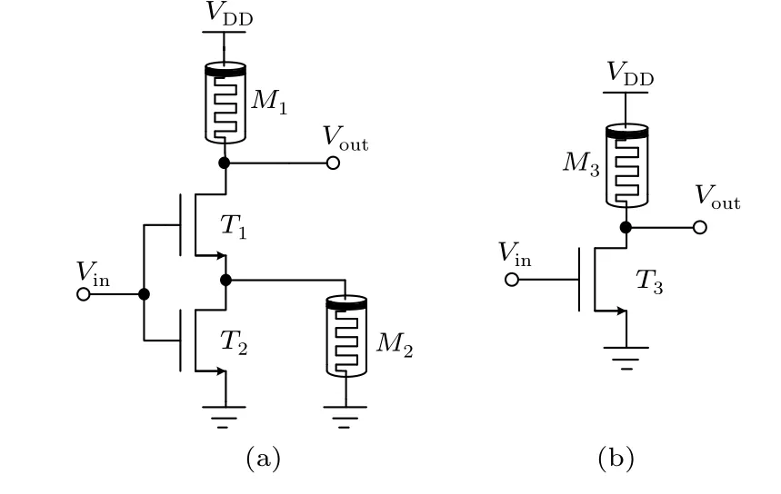
Fig.8. (a)STI,(b)PTI,NTI in Ref.[63].

Fig.9. Three-input(a)TMIN and(b)TMAX in Ref.[63].
Reference [65] proposed memristor-CNTFET hybrid circuit-based ternary basic logic gates, realized TNAND and TNOR by cascading an STI after TAND and TOR, and then designed some arithmetic circuits. Compared with the circuit that only uses CNTFET,the circuit delay and circuit complexity are lower. In Ref. [66], Mohammedet al.proposed an STI by using memristor and CNTFET. After introducing the memristor into the circuit design, the circuit area and power consumption have been reduced,and the stability has been improved.
3.3.2. Taking the voltage value as logic variable
Reference [67] proposed a ternary logic gates design method using the resistance of a tri-value memristor as the logic variable.The memristor has three stable resistance statesRON(50 Ω),RMED(400 Ω),ROFF(1000 Ω),which correspond to the logic ‘2’, ‘1’, and ‘0’ of the unbalanced ternary logic.The switching of the resistance state is realized by controlling the width and amplitude of the current pulse flowing through the memristor. Both TAND and TOR circuits are composed of three memristors, two of which are used as input memristors and the other is used as output memristor. The initial states of the input memristors are inputs of the logic gate,and the resistance state of the output memristor is the output after the operation. Under different input conditions,the resistance value of the output memristor will be converted accordingly. In addition, the inverter and COPY circuit are designed. Among them,three types of inverters can be realized by the same NOT circuit structure. The difference lies in the threshold value of the threshold switch used. The COPY circuit can replicate the resistance state of the input memristor.
In 2021, reference [68] proposed a voltage-controlled tri-value memristor model, and then further designed ternary AND,OR,and NOT gate circuits based on it. The memristor model also has three stable resistance statesRH(10 kΩ),RM(1 kΩ), andRL(100 Ω), corresponding to logic ‘0’, ‘1’, and‘2’,respectively.The ternary AND,OR,and NOT gate circuits are shown in Figs.10–12. The ternary AND gate and the OR gate contain three tri-value memristors,two as input memristors and the other as output memristor. The ternary NOT gate is composed of two memristors and an auxiliary resistor. The three ternary inverters are all realized by the same NOT circuit structure,but the value of the auxiliary resistorRand the control voltageVOPare different. In each different input combination, the voltage at both ends of the output memristor is different,so its resistance will switch accordingly.

Fig.10. TAND in Ref.[68].
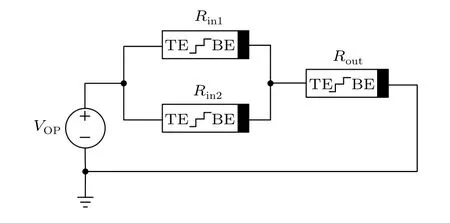
Fig.11. TOR in Ref.[68].

Fig.12. NOT in Ref.[68].
3.4. Design of ternary logic gates based on other technical solutions
In addition to the above-mentioned technical solutions for designing ternary basic logic gates, some other methods have also been able to design ternary gates,such as QDGFET(quantum dot gate field effect transistors),RTD(resonant tunneling diodes), and SET (single electron transistor).[69–71]In 2019, reference [72] produced a ZnO three-state memristor,which can realize 27 kinds of single ternary logic with only one memristor unit, and can further design ternary arithmetic circuits with AND and OR.Similarly,reference[73]proposed an all-optical single-input ternary logic system that can realize all possible 27 single-three-valued logic functions.
With the continuous progress of the semiconductor material industry, more and more semiconductor devices have shown great potential for application in ternary logic circuits.[74]In Ref. [75], a complementary inverter structure based on P-type black phosphorous and N-type molybdenum disulfide transistors was mentioned, which can work in both binary and ternary states. In addition, the application of GNRFET(graphene nanoribbon field effect transistor)in ternary logic has also attracted much attention. GNRFET has higher tensile strength and better durability than CNTFET.[76]In Refs.[77–81],the basic ternary logic gates designed based on GNRFET were studied. Compared with the circuits designed based on CMOS and CNTFET technology, it has significant improvement in power consumption, circuit area, and power delay product(PDP).
4. Several general methods for the design of ternary combinational logic circuits
The ternary basic logic gates introduced in Section 3 are the basic units that constitute ternary combinational digital logic circuits,which can realize decoder,encoder,adder,multiplier, etc. The general methods of ternary combinational logic circuits are summarized below.
4.1. Decoder-encoder method
The process of designing ternary combinational logic circuits is mainly divided into three steps. First, decode the ternary input into the binary form,then use the binary to perform the corresponding operation, and finally, convert the binary to the ternary output. Figure 13 shows the block diagram of this process. In most of the existing designs, the final encoder part is composed of a level shift circuit and a ternary OR gate, rather than an encoder circuit in the traditional sense. In this section,we will first introduce the design of the decoder and encoder, and then give a brief introduction to the ternary combinational logic circuits based on the decoder-encoder method.

Fig.13. Block diagram of decoder-encoder method.
4.1.1. Design of ternary decoder and encoder
The function of the decoder is to convert a ternary signal into a binary signal. As shown in Table 3, it is the truth table of a general ternary decoder. In Refs.[5,63,82],a decoder with the general logic structure was implemented based on the designed basic logic gates,as shown in Fig.14. In Ref.[51],a novel decoder structure was proposed,compared with the general design scheme in Fig.14,the number of components used has notably reduced. In 2020,reference[67]designed a novel decoder structure based on ternary basic logic gates. Contrary to the truth table in Table 3, this circuit uses logic ‘0’ as the effective level to output. Reference [83] proposed a 1–3 line decoder and a 2–9 line decoder based on ternary memristor-CMOS logic gates, and synthesized on FPGA development board.
The encoder can convert the intermediate binary signal into the final ternary output.Reference[84]proposed a ternary encoder based on CNTFET,the circuit is optimized at the transistor level, and the simulation results show that it performs well in terms of delay,power consumption,and the number of transistors. In 2016, reference [85] proposed and designed a 9–2 ternary reversible encoder and a 9–2 ternary reversible priority encoder,and it plays a role in the conversion of a binary circuit and a ternary circuit. In 2018, Vudadhaet al.[86]proposed an improved encoder based on CNTFET,and applied it to the design of ternary combinational logic circuits. The simulation results show that the power consumption,propagation delay, and power delay product of the ternary full adder designed based on the proposed encoder have been significantly improved. In addition,reference[63]mentioned a ternary encoder based on memristor and CMOS,which can convert three binary signals into one ternary signal.

Table 3. Truth table of ternary decoder.

Fig.14. General ternary decoder structure.
4.1.2. Ternary combinational logic circuits based on decoder-encoder method
In 2020, reference [87] proposed a half adder based on memristor and CNTFET using the decoder-encoder method,as shown in Fig. 15, and then three different full adders have been designed,including CRA(carry-ripple adder),CLA(carry-lookahead adder), and CSA (carry-skip adder). Reference [88] also used this method to design a one-bit ternary comparator,which can be further expanded into anN-bit comparator. References[89–91]also designed a variety of ternary combinational logic circuits with different functions using this method.
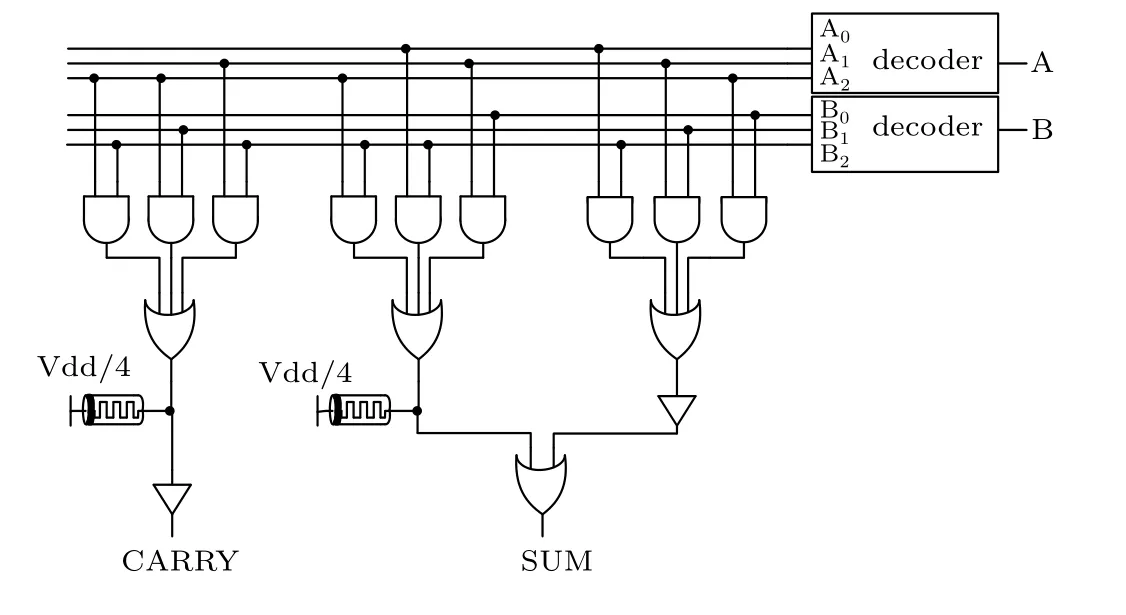
Fig.15. Half adder designed by decoder-encoder method in Ref.[87].
4.2. Multiplexer-based method
In a ternary logic system,the multiplexer(MUX)can select a signal from multiple ternary digital input signals and output it. Table 4 shows the truth table of the 3:1 MUX,Sis the selection signal,I0,I1,andI2are three input signals.
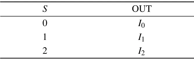
Table 4. Truth table of 3:1 MUX.
When it comes to the design of ternary combinational logic circuits based on multiplexers,some of the input signals can be used as the MUX selection signal,and the remaining input signals or their unary functions can be used as the inputs of the MUX.Among them,MUX can be designed with a variety of technologies, and the corresponding ternary logic function can be realized through the combination of multiple MUXs and ternary single-variable logic circuits. The advantage of this method is that the circuit can be designed without ternary basic logic gates‘AND’,‘OR’,‘NOT’,etc.,but only uses the combination of ternary unary operators and multiplexers for implementation,which can reduce the power consumption of the circuit and the number of components.
In Ref.[92],Jaberet al.designed a novel MUX based on CNTFET, and then proposed a half adder with 90 transistors only using the MUXs,as shown in Fig.16. In the same year,the author used this method to design a ternary multiplier in Ref.[93]. The simulation results show that the proposed multiplier reduces power consumption and improves noise tolerance. Reference[94]used two-stage multiplexers to design a full adder unit. In the first stage, the carry inputCinfrom the lower bit behaves as selection signals of the three 2:1 MUXs,and the unary functions of one inputAare used as the inputs of the first stage;3:1 MUX from the second stage uses another inputBas the selection signal, and the inputs are the outputs of the three 2:1 MUXs in the first stage. Reference[95]mentioned a method of using two 2:1 MUX to form a 3:1 MUX,and only used 2:1 MUX to design a ternary half adder. In addition, references [96–99] also used this method to design ternary functional combinational logic circuits.

Fig.16. Half adder designed only using MUXs in Ref.[92].
4.3. Transistor level method
The design idea of this method is to use the logic level of the input signal or the unary functions of the input signal to directly control the conduction of the transistors,in other words,under each group of input,there will be a corresponding path connected to the output terminal to get the required logic level at the output.

Fig. 17. Ternary full adder carry circuit using transistor level method in Ref.[100].
For example,in Ref.[100],a ternary full adder carry circuit was designed based on CNTFETs, which is to directly control the conduction of CNTFETs through the unary function of inputA,B, andCin. For each group of inputs, there will be a path that appears in the circuit, so as to transfer the corresponding logic level to the output. Figure 17 shows the structure of the carry circuit, where the diameter ofT1–T17isd=1.487nm, the diameter ofT18andT19isd=1.108 nm,and the diameter ofT20–T33isd=0.783 nm,different transistor diameters correspond to different threshold voltages. This method does not require the use of basic logic gate circuits either, and the proposed circuit has a lower critical delay, a lower PDP, and a higher operating frequency, the number of transistors used is also greatly reduced. However, the design of a ternary logic circuit with this method will not progress from basic to complex. Each input situation needs to be taken into consideration separately, so the design idea is relatively complicated. Reference [101] designed a ternary comparator through this method, and the power consumption and propagation delay were greatly reduced compared with the previous design. Transistor-level methods can greatly reduce the number of transistors used and have been concerned and used by many researchers.[102–110]
4.4. Other methods
In Ref. [111], a method of using transmission gates was described, that is, the input signal or unary functions of the input are used as the control signal of the transmission gates.Under each group of inputs, there will be a correct path connected to the output, similar to the transistor level method without a decoder. References[112,113]both used a method of capacitance threshold logic,that is,to sum the input by the analog ratio based on capacitance,controlled by the threshold detection circuit, instead of the traditional decoder function.Reference [18] proposed a ternary full adder unit designed with a dynamic ternary logic style.
5. Ternary sequential logic circuits
The output of a ternary combinational logic circuit only depends on the current external input, so the relationship between output and input can reflect the function of the circuit.Several design methods mentioned in Section 4 can realize it with the corresponding functional relationship. However, the output of the sequential circuit is not only related to the current external input but also the previous output.That makes the storage element ternary flip-flop become the first step on the ternary sequential logic circuits implementation. Compared with binary flip-flops, ternary flip-flops have more complex logic functions. In addition,ternary flip-flops not only can be driven by a binary clock, but also can be driven by a ternary clock. When designing a ternary flip-flop,you cannot just replace the logic gates required by a binary flip-flop with the ternary logic gates. This may lead to incomplete functions.Therefore,the circuit structure of the ternary flip-flop may be slightly more complex than that of the binary flip-flop. This section first summarizes the related design of the ternary flipflops and then introduces two commonly used sequential circuits registers and counters.
5.1. Ternary FFs
Similar to binary flip-flops,ternary flip-flops can also be divided into many types, such as D flip-flop, T flip-flop, and JK flip-flop.[114]Besides, there are PZN flip-flop, JKL flipflop,etc.[115,116]
In 1977, reference [115] designed ternary basic logic gates based on MOSFET,and then further designed a ternary D flip-flop, a T flip-flop, and a PZN flip-flop. It is worth noting that the clock signal of the designed flip-flop has only two logic levels, logic ‘0’ and logic ‘2’. Reference [116] designed a series of ternary basic module circuits,such as 1-of-2 threshold-tmultiplexing and identity cell, and then designed ternary D flip-flop and JKL flip-flop based on these module circuits. In addition, references[117–119]also proposed different implementations of D flip-flops based on CMOS technology. Among them,the D flip-flop in Ref.[117]uses a latch and a neuron-CMOS literal circuit, reference [118] describes a new CMOS edge-triggered ternary D flip-flop based on double pass-transistor logic (DPL), the D flip-flop mentioned in Ref.[119]has a reset port.Reference[120]describes a ternary D flip-flop based on multiple-junction surface tunnel transistor(MJSTT) and MOSFET. The number of components used in this flip-flop is reduced from 30(only using MOSFETs)to 3,thus greatly reducing the circuit’s area consumption.
In 2010, reference [121] proposed two types of edgetriggered master-slave D flip-flops based on ternary basic logic gates. One is controlled by a binary clock, and the other is controlled by a ternary clock. But there is no specific circuit realization in the article. Instead, the simulation operation was carried out with SIMULINK. In 2016, reference [122]proposed a ternary JK flip-flop based on RTD, which realized the pre-set function. With the literal circuit as the core of the mathematical deduction process, it is much easier to realize the circuit. In the same year, reference [123] proposed two kinds of JKL flip-flops based on CNTFET, one is a single-edge trigger, and the other is a double-edge trigger.In 2017, reference [124] proposed a ternary pulsed D flipflop with a reset port and a set port. In 2019, Katayounet al.[125]proposed a D flip-flop based on successor and predecessor circuits, which is useful in the design of a ternary counter with lower complexity. Reference [4] mentioned a CNTFET-based quad-edge-triggered ternary flip-flop, which is composed of four types of basic logic blocks: ternary clock driver,standard ternary inverter,binary inverter,and transmission gate. In 2020,Zarinet al.[126]designed a ternary D latch based on GNRFET,and then designed a ternary positive edgetriggered master-slave D flip-flop. In 2021, reference [127]employed gate-all-around (GAA)-CNTFET and nonvolatile magnetic tunnel junction(MTJ)to design two types of ternary retention flip-flops: basic ternary retention flip-flop and input aware ternary holding flip-flop. In the proposed input aware ternary retention flip-flop, the power consumption is significantly reduced by adding a magnitude comparator and preventing duplicate data transfer to the MTJs.
5.2. Register
Reference [115] mentioned a two-stage dynamic ternary shift register,where each stage is composed of two STI gates and two ternary switches. In 2002, reference [120] formed a ternary shift register by cascading the ternary D flip-flops that designed. Reference[119]designed a ternary adiabatic D flip-flop with a reset port and a ternary adiabatic multiplexer at first,and then designed a ternary adiabatic shift register,which can realize left shift,right shift,input,and output in parallel of the ternary signal under the control of the clock. In 2021,reference[127]designed a four-trit non-volatile universal ternary shift register based on the proposed non-volatile ternary retention flip-flop. The circuit consists of four ternary retention flip-flops and four 8 to 1 multiplexers, which can realize the functions of input and output in parallel,left shift,right shift,hold,set‘0’,set‘1’,set‘2’,toggle and restore.
5.3. Counter
In 1977, reference [115] cascaded the designed ternary master-slave D flip-flop, and fed back the outputQnof the last stage D flip-flop to the input terminalD1of the first stage to form a ring ternary counter,nis the number of flip-flops.Then, the article also gave a 3-trit ternary counter that can count from 0 to 27 or from−13 to+13. This counter consists of three master-slave T flip-flops and two NIT gates. Finally,based on the ternary counter formed by T flip-flops,a divideby-M ternary counter was proposed with a feedback circuit.Reference [116] designed a modulo-9 up counter based on the designed ternary D flip-flop and ternary basic logic operation circuits. In 2017,Kanget al.[124]constructed a four-digit ternary reversible counter based on the designed D flip-flop,up/down circuit, and carry/borrow controlled circuit. After HSPICE simulation analysis, the results show that the proposed circuit attains the average energy saving by 36.4%compared with the ternary counter based on JKL flip-flop, so the low power consumption characteristics of the counter are obviously. In 2019,reference[125]designed a three-trit ternary asynchronous counter and a synchronous counter on the basis of the proposed SP-D flip-flop. The circuit structure diagrams are shown in Figs.18 and 19,respectively.
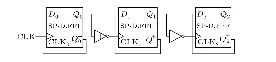
Fig.18. Three-digit ternary asynchronous counter in Ref.[125].
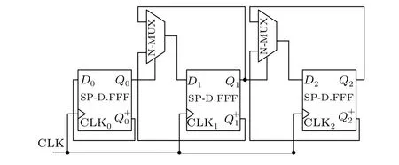
Fig.19. Three-digit ternary synchronous counter in Ref.[125].
6. Conclusion
With the further development of modern information technology, the integration of devices continues to increase,and problems such as interconnection and excessive power consumption have become more prominent. Ternary logic has a better effect on solving these problems.Furthermore,ternary logic carries more information and can increase the data density of the circuit compared with binary logic. Therefore,it is a promising alternative to the traditional binary logic circuit.It is worthy of further research and discussion by scientific and technological workers. In subsequent research, we can continue to explore the production of new materials and new components for ternary logic circuits, and use these devices to build functional ternary circuits. There are few pieces of researches on balanced ternary circuits at present,and the application of balanced ternary circuits can be further explored to give full play to its unique advantages. In addition,in-depth research can be done on the ternary computer architecture system,hoping that the ternary logic circuits can be widely used as soon as possible.
杂志排行

Chinese Physics B的其它文章
- Transient transition behaviors of fractional-order simplest chaotic circuit with bi-stable locally-active memristor and its ARM-based implementation
- Modeling and dynamics of double Hindmarsh–Rose neuron with memristor-based magnetic coupling and time delay∗
- Cascade discrete memristive maps for enhancing chaos∗
- Extended phase diagram of La1−xCaxMnO3 by interfacial engineering∗
- A double quantum dot defined by top gates in a single crystalline InSb nanosheet∗
- Discontinuous and continuous transitions of collective behaviors in living systems∗