Thermally induced band hybridization in bilayer-bilayer MoS2/WS2 heterostructure∗
2021-05-24YanchongZhao赵岩翀TaoBo薄涛LuojunDu杜罗军JinpengTian田金朋XiaomeiLi李晓梅KenjiWatanabeTakashiTaniguchiRongYang杨蓉DongxiaShi时东霞ShengMeng孟胜WeiYang杨威andGuangyuZhang张广宇
Yanchong Zhao(赵岩翀), Tao Bo(薄涛), Luojun Du(杜罗军), Jinpeng Tian(田金朋),Xiaomei Li(李晓梅), Kenji Watanabe, Takashi Taniguchi, Rong Yang(杨蓉), Dongxia Shi(时东霞),7,‡,Sheng Meng(孟胜),3, Wei Yang(杨威),3,7,§, and Guangyu Zhang(张广宇),3,7,¶
1
Beijing National Laboratory for Condensed Matter Physics;Key Laboratory for Nanoscale Physics and Devices,Institute of Physics,Chinese Academy of Sciences,Beijing 100190,China
2School of Physical Sciences,University of Chinese Academy of Sciences,Beijing 100190,China
3Songshan Lake Materials Laboratory,Dongguan 523808,China
4Department of Electronics and Nanoengineering,Aalto University,Tietotie 3,FI-02150,Finland
5Research Center for Functional Materials,National Institute for Materials Science,1-1 Namiki,Tsukuba 305-0044,Japan
6International Center for Materials Nanoarchitectonics,National Institute for Materials Science,1-1 Namiki,Tsukuba 305-0044,Japan
7Beijing Key Laboratory for Nanomaterials and Nanodevices,Beijing 100190,China
Keywords: two-dimensional materials, transition metal dichalcogenides (TMDs) heterostructure, band hybridization,interlayer exciton
1. Introduction
Monolayer transition metal dichalcogenides (TMDs) are an atomically thin semiconductor with inversion asymmetry and strong spin–orbit coupling(SOC),[1]the associated spinand valley-dependent selection rules result in a plethora of unique optical properties.[2–4]By stacking TMDs heterostructures with a type II band alignment,[5–7]it favors ultrafast charge transfer of electrons and holes to different layers after optical excitation, and eventually leads to a formation of long-lived interlayer exciton in the low energy range.[8,9]Recent focus has been placed on finding and understanding the collective behaviors induced by the strong electronic interactions in this system. Similar to twisted bilayer graphene,[10,11]twisted TMDs structures offer an unique platform to engineer the electronic band structure and the emergent optical properties.[9,12–14]Though excitonic effects and optical spectra have been studied in many experiments, the results vary greatly even for the same type TMDs heterostructure. The observed phenomenon disunion in experiments strongly suggests a delicate interplay between the crystal lattice, interlayer coupling, band hybridization, and moir´e effect in the heterostructures.[9,14–22]A feasible way to engineer such interplay as well as the electronic/optical properties of TMDs heterostructures is badly in need for the application in the area of optoelectronics and valleytronics.
Here we study the photoluminescence (PL) spectra of near 0◦aligned bilayer-bilayer MoS2/WS2heterostructures,and demonstrate thermal annealing as an effective means to induce hybridization effects in commensurate van der Waals heterostructures. By employing thermal annealing,we observe a more efficient interlayer charge transfer in the heterostructure indicating a stronger interlayer coupling. Moreover, the PL spectra in the low energy range undergo the transition from multiplet narrow emissions dominated by periodic moir´e potential to a couple of emissions dominated by hybridized electronic states. The electric controllability and valley-dependent polarization of the interlayer exciton are also revealed.Our results indicate that after thermally induced band hybridization the heterostructure behaves more like an artificial new solid,rather than just the combination of two individual TMD components.
2. Sample preparation
Figure 1(a) shows a schematic diagram of our device,we prepare h-BN encapsulated near 0◦aligned bilayer-bilayer MoS2/WS2heterostructure with few-layer graphene(FLG)as top gate by van der Waals-mediated dry transfer approach employing propylene carbonate (PC) stamp.[23,24]Firstly, FLG,h-BN, bilayer MoS2, and bilayer WS2flakes are exfoliated onto SiO2(300 nm)/Si substrate.And then PC stamps are used to pick up h-BN flake,bilayer MoS2,bilayer WS2,and another h-BN flake in sequence with accurate alignment based on an optical microscope. The sandwiched structure is then transferred onto SiO2(300 nm)/Si substrate, and finally another FLG is transferred on it as a top gate by dry transfer technique.Finally,metal contacts to the heterostructure and FLG are patterned by the standard micro-fabrication processes including e-beam lithography (EBL), metal evaporation Ti (3 nm)/Au(40 nm), and lifting-off. Figure 1(b) shows an optical image of the device, where the bilayer MoS2and bilayer WS2are sketched by red and black dotted lines,respectively.
3. Results and discussion
Micro-photoluminescence (PL) measurements are performed on the as-prepared heterostructure,the sample is held at 10 K and excited under a continuous-wave 532 nm laser with a spot size of 1.5 µm. The blue curve in Fig. 1(c)shows the PL spectra in the energy range of intralayer excitons. The heterostructure shows three dominated PL peaks,which we attribute to the indirect exciton of bilayer MoS2or WS2(∼1.53 eV),neutral A exciton(A0)of WS2(∼1.98 eV),A0and its negatively charged exciton (A0) of bilayer MoS2(∼1.92 eV), respectively. The blue curve in Fig. 1(d) shows the PL spectra in the energy range of interlayer excitons for the twisted bilayer-bilayer MoS2/WS2heterostructure. By using Gaussian functions to fit the spectra we get multiplet emissions from several nearly equally spaced interlayer exciton resonances,and the averaged full width at half maximum(FWHM) of the emissions is 22.4 meV, these behaviors are the signature of interlayer excitons trapped in moir´e potential(Fig.S1). Our results demonstrate that except for monolayermonolayer case,moir´e interlayer exciton can also manifest in the twisted bilayer-bilayer TMDs heterostructure.

Fig.1. (a)Schematic diagram for the bilayer-bilayer MoS2/WS2. (b)Optical image of the heterostructure. (c)Low temperature PL spectra of intralayer excitons for bilayer-bilayer MoS2/WS2 heterostructure before and after thermal annealing. (d), (e)Low temperature PL spectra of interlayer excitons before and after thermal annealing,respectively.

Fig.2. (a),(b)Calculated band structure of bilayer MoS2 and WS2 with orbital analysis in presence of SOC,respectively. (c),(d)Calculated band structure of 0◦and 180◦twist angle bilayer-bilayer MoS2/WS2 heterostructures with orbital analysis in presence of SOC,respectively.
In order to study the influence of thermal annealing on the electronic band structure and light–matter interaction of the heterostructure, we anneal the sample in the Ar/H2atmosphere at 300◦C and then perform PL measurements. The red curve in Fig. 1(c) shows the exciton PL spectrum after thermal annealing in the intralayer range. The emission intensities of WS2A0exciton (∼1.98 eV) as well as the intralayer indirect exciton(∼1.53 eV)are drastically quenched,indicating a stronger interlayer coupling and more efficient interlayer charge transfer. Moreover, the multiplet emissions of the interlayer excitons(Fig.1(d))vanish after thermal annealing,instead two prominent PL peaks emerge with energy red shift as shown in Fig.1(e).The two emerging peaks show much larger line width and weaker intensity,distinct from the emission of moir´e exciton whose line width is relative narrow.Besides,we perform the PL measurement at different sites of the sample,such two peaks can be detected throughout the heterostructure(Fig. S2), suggesting such transition induced by thermal annealing is universal.
PL spectroscopy tools give access to details of the electronic band structure of the heterostructure,the distinct behavior of intra- and inter-layer excitons before and after thermal annealing indicates that thermal annealing alters the interlayer coupling of the van der Waals heterostructure and greatly induces band hybridization. Note that thermally induced rotation has been demonstrated in graphene/h-BN system.[25]Similarly,one can expect that two small angle twisted bilayers studied here will tend to align with each other during thermal annealing. Significantly,due to the small lattice mismatch between MoS2and WS2,the heterostructure will be commensurate at near 0◦(180◦)twist angle,with the smallest layer separation and nearly ideal R-type (H-type) stacking geometries that free of moir´e effect (Fig. S3). Moreover, the increased interlayer coupling will induce giant hybridization, the hybridization strongly modifies the bands structure and induces band shift,as a consequence,the heterostructure behaves more like a new solid rather than just the combination of two individual TMD components.
To better understand the hybridized band structure of the bilayer-bilayer MoS2/WS2heterostructure, we perform density wave functional theory(DFT)calculation.The band structures of pristine bilayer MoS2(WS2) are shown in Figs. 2(a)and 2(b), where an indirect band gap of 1.31 eV(1.39 eV)is consistent with literature.[26–28]Similarly, the band structure of a closely aligned bilayer-bilayer MoS2/WS2heterostructure is calculated and shown in Figs.2(c)and 2(d)for 0◦and 180◦, respectively. The calculated results show typical type II band alignment with charges distributed in different layers,and no obvious difference is found between the two alignments. Crucially, the interlayer coupling results giant interlayer hybridization so the band structure of the heterostructure is not merely the superposition of the two components. Unlike monolayer MoS2/WS2heterostructure that has been studied widely, the optical transition of interlayer exciton in bilayerbilayer MoS2/WS2heterostructure is more complicated due to the presence of multiple indirect transitions at high symmetry points in the Brillouin zone. The electrons prefer to stay at Kcand Qcvalley of the conduction band(Qcis the energy minimum along Kcto Γc),while the holes tend to occupy the Γvand Kvvalley of the valance band,giving rise to multiple relaxation paths of interlayer exciton. Specifically, there are three possible indirect transitions, i.e., Γv–Qc, Γv–Kc, Kv–Qc, and one direct Kv–Kctransition. Hence, the observed two prominent interlayer excitons in bilayer-bilayer MoS2/WS2heterostructure after thermal annealing might correspond to different intrinsic relaxion transitions with electrons and holes residing in different valleys of the Brillouin zone.
The spatially indirect interlayer exciton possesses an outof- plane electric dipole and can couple to the static electric field. When applying a vertical electric field E, an interlayer exciton exhibits linear Stark shifts, and the magnitude of the Stark shift is given by ∆= µE, where µ =ed is the intrinsic dipole moment and d is the vertical displacement of the electron–hole pairs.[29]As the wavefunction distributions of electrons and holes are quite different at each critical point in the Brillouin zone,the electron–hole separations for interlayer excitons with different transitions have corresponding variational parameters. Therefore, it is an effective way to distinguish the transition paths of interlayer excitons by comparing their dipole-moment values.
Figure 3(a)shows the PL spectra at different top gate voltages, and their interlayer nature is revealed from the Stark effect in the linear shift of the peak (black dotted line in Fig. 3(b)). Labeled as IX1 and IX2, the two interlayer excitons exhibit significantly different linear slops of Stark shift(Fig. 3(b)). The IX1 is red shifted from 1.34 eV to 1.21 eV while IX2 is from 1.35 eV to 1.29 eV as the top gate voltage is changed from 6 V to −4 V.This clearly indicates that the two interlayer excitons are distinct with different dipole-moments as well as different electron–hole separations. In our experiments the ratio of µ between IX1 and IX2 is 2.1, estimated from the dashed lines in Fig.3(b). It should be noted that the top gate will not only induce an out of plane electric field but will also modulate the charge density of the heterostructure leading to the variation of the PL intensity.
Comparing the experimental data to the DFT calculation,we ascribe IX1 and IX2 to Kv–Kcand Kv–Qctransitions, respectively. We firstly rule out the Γv–Qcand Γv–Kcindirect transitions, whose gaps are 1.01 eV and 1.1 eV, respectively.This is because given the large binding energy (∼0.2 eV) of interlayer exciton in TMD heterostructures,[30,31]the exciton energy of Γv–Qcand Γv–Kctransition is so small (< 1 eV)that beyond our detection range. According to the previous results in twisted monolayer-monolayer MoS2/WS2heterostructure,the ratio of the Stark shift for Kv–Kcto that for Kv–Qcis around 2.39, which agrees well with the ratio of IX1 to IX2.In this regard,we tentatively assign the interlayer IX1 and IX2 to Kv–Kcand Kv–Qctransitions,respectively.
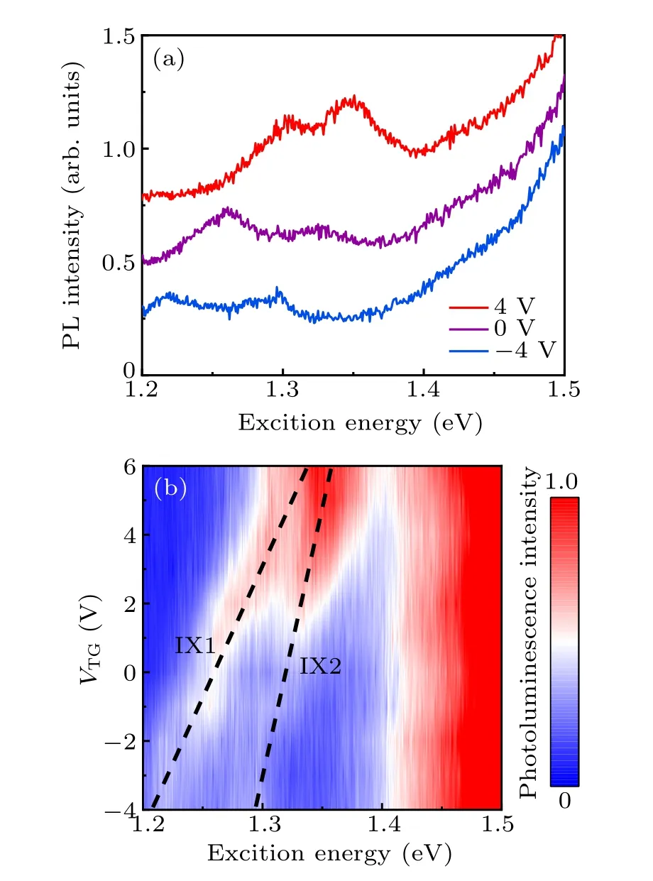
Fig. 3. (a) Gate dependence of the interlayer excitons under 532 nm excitation. (b) Color map of interlayer excitons photoluminescence as a function of applied gate voltage. The black dashed lines are guides to the eye indicating the Stark shift of interlayer excitons IX1 and IX2.
To further confirm the origin of IX1 and IX2, we perform polarization-resolved PL spectra and study their valleydependent polarization selection rules. Figures 4(a) and 4(c)(4(b) and 4(d)) show the polarization-resolved PL spectra of interlayer(intralayer)excitons at 10 K,excited by 532 nm circularly polarized light. It is clearly shown that the interlayer excitons possess robust negative circular polarization,whereas the intralayer A0and A−excitons have the positive dichroism,indicating the opposite chirality between them. More significantly, IX1 is totally suppressed and indistinguishable with background under co-circularly polarized detection. We thus quantify them by the degree of circular polarization,defined as Pc=(I+−I−)/(I++I−),where I+(I−)denotes the intensity of the co-polarized (cross-polarized) PL component with the excitation. While IX2 shows relatively small negative circular polarization,IX1 gives giant negative circular polarization that exceeds 65%(inset of Figs.4(a)and 4(c)).
Such distinct difference of circular polarization between IX1 and IX2 can be interpreted as a result of their relaxation paths, which also confirms our expectation on their origin.Circular polarization is locked with the spin polarization in the heterostructures,and it varies dramatically between different stacking order at atomic scale and different valley of the Brillouin zone.[32]For both the conduction and valance bands around K valley, the corresponding Bloch wavefunctions are in-plane, predominantly from the d orbitals of Mo and W atoms. Consequently, interlayer hopping between the upper and lower layers is small, which, together with site dipolefield, largely enhances the spin-polarization effects. Therefore,the IX1 exciton,which corresponds to the transition between Kvand Kcvalleys, exhibits large circular polarization.However, the IX2 corresponds to the transition between Kvand Qcvalleys,as the considerable out of plane pzcharacter of chalcogens at Q valleys leads to significant interlayer hopping and seriously weakens the spin-polarization, which gives rise to the exhibiting relatively small circular polarization.[33–35]
At last, we point out that, compared with monolayermonolayer case,[36]in bilayer-bilayer TMD heterostructure layer number as a new degree of freedom will bring more unique phenomenon to the system. Apart from the layer dependent band structure, which will bring infrared directand indirect-interlayer excitons that we have demonstrated here, electric modulated spatial wavefunction distributions of the bounded electrons and holes between the layers are also expected. Such controllability under the quantum confined regime combining with the spin-layer locking effect makes bilayer-bilayer TMDC heterostructure a promising platform to study Bose–Einstein condensation and dissipationless exciton.
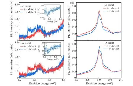
Fig. 4. Polarization-resolved PL spectra near the interlayer (a) and intralayer (b) excitons of the bilayer-bilayer MoS2/WS2 heterostructure using+σ (top)and −σ (bottom)excitation of 532 nm. The insets in(a)show the calculated circular polarization of interlayer excitons.
4. Conclusion and perspectives
In conclusion,we demonstrate that thermal annealing can increase interlayer coupling in the van der Waals heterostructures,and after thermally induced band hybridization such heterostructure behaves more like an artificial new solid, rather than just the combination of two individual TMD components.We carry out experimental and theoretical studies of excitons in near 0◦aligned bilayer-bilayer MoS2/WS2heterostructure with strong interlayer coupling, demonstrate the electric controllable direct and indirect infrared interlayer excitons in such system. Our results reveal the impact of interlayer coupling on the excitonic properties of van der Waals heterostructures,and will also shed light on the understanding and engineering of spin-valley configuration in such system.
猜你喜欢
杂志排行

Chinese Physics B的其它文章
- Corrosion behavior of high-level waste container materials Ti and Ti–Pd alloy under long-term gamma irradiation in Beishan groundwater*
- Degradation of β-Ga2O3 Schottky barrier diode under swift heavy ion irradiation*
- Influence of temperature and alloying elements on the threshold displacement energies in concentrated Ni–Fe–Cr alloys*
- Cathodic shift of onset potential on TiO2 nanorod arrays with significantly enhanced visible light photoactivity via nitrogen/cobalt co-implantation*
- Review on ionization and quenching mechanisms of Trichel pulse*
- Universal memory based on phase-change materials: From phase-change random access memory to optoelectronic hybrid storage*