Dramatic reduction in dark current of β-Ga2O3 ultraviolet photodectors via β-(Al0.25Ga0.75)2O3 surface passivation
2023-02-20JianYingYue岳建英XueQiangJi季学强ShanLi李山XiaoHuiQi岐晓辉
Jian-Ying Yue(岳建英), Xue-Qiang Ji(季学强), Shan Li(李山), Xiao-Hui Qi(岐晓辉),
Pei-Gang Li(李培刚)1,2,†, Zhen-Ping Wu(吴真平)1,2, and Wei-Hua Tang(唐为华)1,2,3,‡
Keywords: β-(Al0.25Ga0.75)2O3/β-Ga2O3,MOCVD,photodetectors,defect passivation
1. Introduction
It is well known thatβ-Ga2O3is a new type of ultrawide band gap semiconductor material. Compared with SiC and GaN, the band gap ofβ-Ga2O3reaches 4.9 eV, which is higher than 3.25 eV of SiC and 3.4 eV of GaN.[1–4]Due to its anti-irradiation and high temperature resistance, it can maintain stable properties in extreme environments such as high and low temperature and strong radiation,and its high breakdown field strength ensures that a preparedβ-Ga2O3device can be used under ultra-high voltage, which is beneficial to improve the carrier collection efficiency.[5,6]Based on these,power devices based onβ-Ga2O3are expected to have higher breakdown voltage and lower on-resistance,resulting in lower conduction losses and higher power conversion efficiency.[7]These characteristics ensure thatβ-Ga2O3is promising to applications in the field of power electronics devices. Furthermore,β-Ga2O3is an ideal candidate for solar-blind ultraviolet(UV)detection due to its wide band gap,large UV absorption coefficient,and easy processing,etc.[8,9]
As we know, wide-bandgapβ-(AlxGa1-x)2O3films would enable higher critical field strength in power electronic devices.[10]Entry of Al elements can effectively modulate the band gap of intrinsicβ-Ga2O3. For example, aβ-(AlxGa1-x)2O3film can adjust the band gap and carrier concentration.[11–13]Also,β-(AlxGa1-x)2O3film can be employed in modulation-dopedβ-(AlxGa1-x)2O3/β-Ga2O3heterostructures,where the separation between the ionized donor impurities and the two-dimensional electron gas would enable higher electron mobilities.[14]Various methods for growth ofβ-(AlxGa1-x)2O3films have been explored, such as molecular beam epitaxy (MBE), pulsed laser deposition (PLD),[15]metal organic chemical vapor deposition (MOCVD),[16]and magnetron sputtering.[17]The earliest documents indicate that,in 2012, Itoet al.[18]used the mist-CVD method to deposit and growα-(AlGa)2O3thin films. In recent years,Milleret al. used TEAl and TMAl as Al sources to perform MOCVD deposition ofβ-(Al0.21Ga0.79)2O3/Ga2O3film superlattice structure.[16]Although theβ-(AlxGa1-x)2O3films have received a certain degree of widespread attention, there are few reports on preparation of detectors for passivatingβ-Ga2O3film surfaces withβ-(AlxGa1-x)2O3films.
In this work,we adjust the ratio of[TMAl]/[TMAl+TEGa]by adjusting the amount of injected TMAl flow, to obtainβ-(AlxGa1-x)2O3/β-Ga2O3films atx= 24.71%. Moreover,theβ-(Al0.25Ga0.75)2O3films are used as surface passivation materials due to their wider band width and excellent optical transmittance. The MOCVD epitaxy only needs to cut into the TMAl source to continuously grow without taking out the chamber and then to coat the film with plasma enhanced chemical vapor deposition (PECVD) or other coating equipment,for simultaneously reducing air water oxygen pollution,achieving high quality interfacial continuation, reducing surface defects and high lattice match withβ-Ga2O3. We explore the change and mechanism of detection performance of theβ-Ga2O3film detector afterβ-(Al0.25Ga0.75)2O3surface passivation. It is found that under illumination with 254 nm light at bias 5 V,theβ-(Al0.25Ga0.75)2O3/β-Ga2O3photodetectors(PDs) show low dark current and high current on/off ratio,the dark current is sharply reduced by about 50 times after passivation of theβ-Ga2O3surface, and current on/off ratio increases by approximately 2 times. The results show thatβ-Ga2O3detectors withβ-(Al0.25Ga0.75)2O3surface passivation offer superior detector performance andβ-(Al0.25Ga0.75)2O3has great potential applications as a passivation material in the field of ultraviolet photoelectric detection.
2. Experiment
In experiment, we investigated growth of (¯201)β-(Al0.25Ga0.75)2O3/β-Ga2O3films on (0001)-oriented sapphire with a low-temperatureβ-Ga2O3buffer at 630°C using a closed-coupled showerhead-MOCVD(CCS-MOCVD).Triethylgallium (TEGa,6N) and trimethylaluminum (TMAl,6N)were used as the metal-organic precursors for Ga and Al, respectively. High purity oxygen and argon (99.999%) were used as the O source and carrier gas. The growth temperature and growth pressure were set to about 750°C and 20 torr.[19]We deposited aβ-Ga2O3film for 30 min,and continued to deposit a 30-minβ-(Al0.25Ga0.75)2O3film on it as a passivation layer. The deposition rates ofβ-Ga2O3andβ-(Al0.25Ga0.75)2O3film were 10 nm/min and 5 nm/min,respectively.The Al composition inβ-Ga2O3set in this work is 25%,which is a commonly used ratio. Metal–semiconductor–metal(MSM) PDs ohmic electrodes were fabricated by a radiofrequency magnetron sputtering,in which Ti 30 nm/Au 80 nm square electrodes films(2×2 mm)were deposition on theβ-Ga2O3andβ-(Al0.25Ga0.75)2O3/β-Ga2O3films. The effective irradiation area is 4 mm2.The crystalline quality of theβ-(Al0.25Ga0.75)2O3/β-Ga2O3films were characterized by highresolution x-ray diffraction (HRXRD, Bruker D8 Discover),and surface morphology were displayed by a field emission scanning electron microscope(FESEM FEI Helios 600). The optical features were investigated by optical diffuse absorption spectra employing a Shimadzu UV-2600 spectrophotometer. Al compositions andβ-(AlxGa1-x)2O3/β-Ga2O3film energy bandgaps were studied by a Thermo Fisher Scientific ESCALAB 250Xi x-ray photoelectron spectroscope (XPS)with AlKαradiation source (h=1486.7 eV). The Keithley 4200-SCS test system was used to characterize the photoelectric performance of the device and is equipped with 254 nm and 365 nm ultraviolet excitation light sources. A Thorlabs PM120VA power meter was used to record and calibrate the light intensity.[20]
3. Results and discussion
The XRDω–2θdiffraction pattern shows that the film has diffraction peaks at 2θ= 18.95°, 2θ= 38.44°and 2θ= 59.08°corresponding toβ-Ga2O3andβ-(Al0.25Ga0.75)2O3/β-Ga2O3films (¯201) (¯402) and (¯603) reflections respectively in Fig. 1(a).[21,22]The calculation of Al composition by XRD is mainly based on Vegard’s law.[11,12,21,23]We approximate that the material is affected by the Al composition in a linear distribution on the lattice constant.[6,18,24]Therefore, we can tell the Al mole fraction based on the peak position shift of theβ-(Al0.25Ga0.75)2O3layer from reference peak position. For instance, forβ-(Al0.25Ga0.75)2O3/β-Ga2O3, the difference of angleθof Al2O3orβ-Ga2O3is Δθ0, the angle shift ofβ-(Al0.25Ga0.75)2O3fromβ-Ga2O3is Δθ,then the Al mole fraction can be given asX=Δθ/Δθ0. The calculated Al component is 24.72%, which approximates our predicted component concentration. Figure 1(b) shows the Ga2O3andβ-(Al0.25Ga0.75)2O3/β-Ga2O3(¯603) diffraction peak, which displays that the (¯603) diffraction peak gradually shifts to a high angle with the merger of Al. This is attributed to the atomic radius of Al smaller than that of Ga,which causes the peak position to gradually shift to a high angle.[5]

Fig.1. (a) XRD pattern of the β-Ga2O3 and β-(Al0.25Ga0.75)2O3/β-Ga2O3 films as grown by MOCVD. The observed (¯201), (¯402),(¯603) diffraction peaks are located at 18.9°, 38.44° and 59.18°, respectively. (b) The (¯603) diffraction peak of the β-Ga2O3 and β-(Al0.25Ga0.75)2O3/β-Ga2O3 films.
Band gaps of theβ-Ga2O3andβ-(Al0.25Ga0.75)2O3/β-Ga2O3films are calculated from the absorption spectrum measurements as shown in Fig.2. With the increase of Al content,the absorption edge of theβ-(Al0.25Ga0.75)2O3/β-Ga2O3film shifts to the direction of short wavelength. The inset in Fig.2 shows the (αhν)2of the film as a function of photo energy,withhνrepresenting the energy of the incident photon,αthe absorption coefficient which is evaluated using the standard relation taking the film thickness into account.[25]The band gaps of theβ-Ga2O3andβ-(Al0.25Ga0.75)2O3/β-Ga2O3films were evaluated by extrapolating the linear region to the horizontal axis, which were 4.99 eV and 5.07 eV, respectively.This indicates that the increase of Al component can cause a significant blue shift of the absorption edge which leads to an increase in the band gap.[26]Typical SEM images(5×5 μm2)in Figs. 3(a) and 3(b) were taken for theβ-Ga2O3andβ-(Al0.25Ga0.75)2O3/β-Ga2O3films. Although the addition of Al slightly affects the lattice constant of theβ-Ga2O3film,the images show that theβ-(Al0.25Ga0.75)2O3/β-Ga2O3film keeps the compactness and flatness of theβ-Ga2O3film.
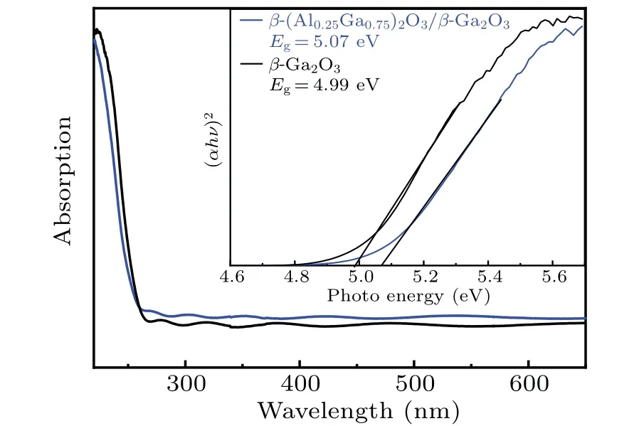
Fig.2.Absorption spectra of the β-Ga2O3 and β-(Al0.25Ga0.75)2O3/β-Ga2O3 films. The Eg of β-Ga2O3 and β-(Al0.25Ga0.75)2O3/Ga2O3 films are given in the inset.
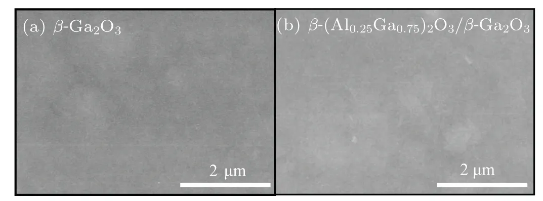
Fig.3. The SEM images (scan area 2×2 μm2): (a) β-Ga2O3, (b) β-(Al0.25Ga0.75)2O3/β-Ga2O3.
X-ray photoelectron spectroscopy (XPS) tests on theβ-Ga2O3andβ-(Al0.25Ga0.75)2O3/β-Ga2O3films are performed to verify the Al content and band gap verification.XPS is usually used to analyze the binding energy of nuclearlevel electrons in materials.[5,22]Wide survey scans in the binding energy range of 0–1200 eV for theβ-Ga2O3andβ-(Al0.25Ga0.75)2O3/β-Ga2O3films were performed as shown in Fig.4(a). The XPS spectroscopy confirms the electron peak of Ga,Al,and O.[15]The peak position is regulated by C 1s of 284.6 eV.Compared toβ-Ga2O3,theβ-(Al0.25Ga0.75)2O3/β-Ga2O3film exhibits the obvious peak shift towards the higher binding energy. The insets in Figs. 4(b) and 4(c) show the high-resolution XPS spectra of Ga 2p3/2and Al 2p core levels for the Ga2O3andβ-(Al0.25Ga0.75)2O3/β-Ga2O3films. From Fig.4(b),Ga 2p3/2core levels of theβ-(Al0.25Ga0.75)2O3/β-Ga2O3films with different Al content are located at 1117.5 eV,which is attributed to the Ga–O bonding.[12,27]The peak intensity gradually increases with the increasing Al content,and no obvious shift is observed. Al 2p peaks of theβ-(Al0.25Ga0.75)2O3/β-Ga2O3films are shown in Fig. 4(c). It is obvious that with the increasing Al content, the diffraction intensity becomes greater and no peaks are observed in theβ-Ga2O3film.This trend reflects the change in the ratio of Al/Ga atoms in the film.In order to verify the chemical state of theβ-(Al0.25Ga0.75)2O3/β-Ga2O3film,O 1s was subjected to Gaussian fitting peak separation processing in Figs. 4(d) and 4(e).O1represents the oxygen atom located in the crystal lattice,and the binding energy is generally at 530.1±0.1 eV;[15,19]O2usually represents oxygen vacancy defects(VO)in the film and the binding energy is generally at 530.8±0.1 eV.[27]The area of each peak can be used to indicate the concentration of the component, and the ratio of O2/(O1+O2) can be used to indicate the concentration of oxygen vacancy defects.[24,27]From Fig. 4(d), it can be seen that the concentration of oxygen vacancy defects decreases from 0.54(β-Ga2O3)to 0.4 ofβ-(Al0.25Ga0.75)2O3/β-Ga2O3. It shows that the Al composition within a certain content can offset the generation of oxygen vacancies, and obtain a low defect concentration in theβ-(AlxGa1-x)2O3film.[12]
Theβ-Ga2O3andβ-(Al0.25Ga0.75)2O3/β-Ga2O3films were utilized to fabricate the MSM ultraviolet photodetector, the current–voltage (I–V) characteristics are measured under dark and 254 nm UV illumination (100 μW/cm) as shown in Fig. 5(a), which includes an inset of schematic diagram of the cross section. However, compared to theβ-Ga2O3devices,theβ-(Al0.25Ga0.75)2O3/β-Ga2O3devices exhibit very low dark current, especially displayed 18 pA (at 5 V bias), which sharply reduces about 50 times. The reason from the analysis may be that the surface passivation ofβ-(Al0.25Ga0.75)2O3/β-Ga2O3reduces the surface state density of the device,surface leakage current decreases,and at the same time,β-(Al0.25Ga0.75)2O3acts as a high-resistance semiinsulating layer, which contributes significantly to the reduction of dark current.[28]In addition, it also benefits from the low oxygen vacancy density of theβ-(Al0.25Ga0.75)2O3/β-Ga2O3epitaxial film. Such a low dark current results in an outstanding current on/off ratio, which is 2.16×10⁵, better than 2.3 times that of theβ-Ga2O3devices. Figure 5(b)shows the switching characteristics (I–tcurve) of theβ-Ga2O3andβ-(Al0.25Ga0.75)2O3/β-Ga2O3devices,meanwhile,the fitting result of the rise and fall times was displayed in Fig.5(b)using the fitted equationI=I0+Ae-t/τ1+Be-t/τ2. It includes the fitting results at the rise time and fall time denoted byτrandτd, respectively.[24,29,30]From Fig. 5(b), all the samples show excellent switching characteristics, the PDs exhibit stable photo current after 4 illumination pulses with a light intensity of 100 μW/cm and a 5 V bias for 20 s. Under 5 V bias,τr/τdfor theβ-Ga2O3andβ-(Al0.25Ga0.75)2O3/β-Ga2O3devices are 5.30/0.09 s and 0.32/0.1 s, respectively. Extremely fast response time for theβ-(Al0.25Ga0.75)2O3passivated devices, 16.56 times faster than theβ-Ga2O3devices.[15,31,32]To further evaluate the detection performance of each device in a comprehensive manner, Fig. 5(c) shows the responsivitiesR, detectivitiesD, and external quantum efficiency(EQE) of the Ga2O3andβ-(Al0.25Ga0.75)2O3/β-Ga2O3devices. Responsivities can be calculated by the following equationR(λ)=(Iλ-Id)/(PλS), in whichR(λ) is responsivity,Iλis the UV-irradiated photocurrent,Idis the dark current,PλandSrepresent the illumination power intensity and effective light area. The other two important PD parameters are obtained according to the formulasD= (R×S1/2)/(2eId)1/2and EQE=Rhc/eλ, withh,c, andebeing the Planck constant,the speed of light,and the charge of electron, respectively.[15,19,20,31,33]The calculated detectivities of theβ-Ga2O3andβ-(Al0.25Ga0.75)2O3/β-Ga2O3devices are 3.49×10¹⁷Jones and 9.26×10¹⁷Jones,respectively. The detectivity of a passivatedβ-Ga2O3detector on the surface is 2.65 times higher than that of aβ-Ga2O3device. Notably,theβ-(Al0.25Ga0.75)2O3passivated device responsivity and EQE have different levels of optimization at bias 5 V and light intensity of 100 μW/cm,the responsivity is 2.8 A/W,and the EQE reaches 3.05×10⁴%. Such a large EQE indicates that the PDs have a large gain,which may be the gain of avalanche.[26,34]
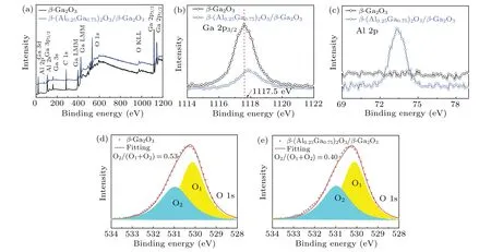
Fig.4. XPS wide scan spectra(a),Ga 2p3/2 (b),Al 2p(c);(d)–(e)XPS spectra of O 1s of the β-Ga2O3 and β-(Al0.25Ga0.75)2O3/β-Ga2O3 films.
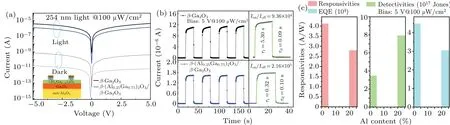
Fig.5. (a) Logarithmic I–V characteristics of MSM photodetectors based on the β-Ga2O3 and β-(Al0.25Ga0.75)2O3/β-Ga2O3 films under dark and light conditions. The inset gives a schematic diagram of the cross-sectional structure of the detector. (b) Logarithmic I–T at 5 V with 254-nm light on/off switching under 100 μW/cm2 and the fitting response speeds for the Ga2O3 and β-(Al0.25Ga0.75)2O3/β-Ga2O3 photodetectors. (c)Responsivity,detectivity,and EQE corresponding to devices of the β-Ga2O3 and β-(Al0.25Ga0.75)2O3/β-Ga2O3 films.
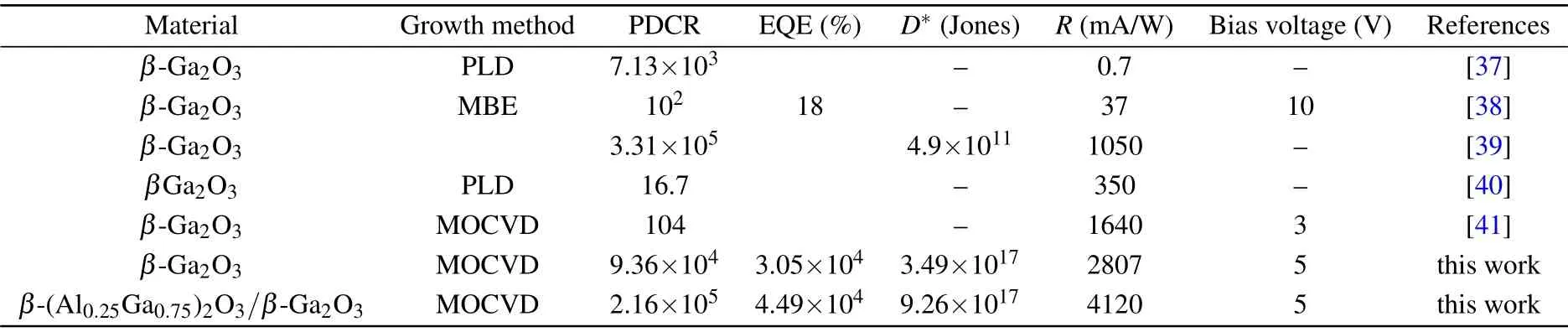
Table 1. Performance comparison of different photodetectors based on the β-Ga2O3 films.
The comprehensive performance comparison with the recently reportedβ-Ga2O3based PDs is shown in Table 1.[35,36]The results prove that theβ-(Al0.25Ga0.75)2O3passivated devices provide a comparable outstanding optoelectronic performance, especially detectivities and external quantum effects compared to theβ-Ga2O3PDs.
To better understand the charge carrier transport mechanism of theβ-(Al0.25Ga0.75)2O3passivated devices,the energy band alignment is shown in Fig.6(a). The energy band position of the device was obtained based on previous reports and optical absorption analysis.[5]Figure 6(b) shows the energy band structure of theβ-(Al0.25Ga0.75)2O3in the dark after contact withβ-Ga2O3. After theβ-(Al0.25Ga0.75)2O3passivation layer grows, the charge carriers keep flowing until the Fermi energy level is homogeneous and the carrier diffusion motion forms a space charge region at the heterogeneous interface,forming a depletion layer and a built-in electric field to maintain the drift and diffusion motion of the equilibrium electron and hole carriers. The highly resistiveβ-(Al0.25Ga0.75)2O3passivation layer grows with few free electrons at the interface and the defect states at the surface are covered,resulting in extremely low dark currents. However,under the UV irradiation at 254 nm,a large number of electron–hole pairs are generated,and the transport mechanism for carriers is greatly changed as shown in Fig. 6(c). When the photogenerated electron–hole pair drifts and diffuses into the built-in electric field,the electrons and holes are rapidly separated and converted into free carriers. The free electrons are transferred from theβ-Ga2O3to theβ-(Al0.25Ga0.75)2O3,and the holes are drifted from theβ-(Al0.25Ga0.75)2O3to theβ-Ga2O3and collected at the Ti/Au electrode under the action of electric field.
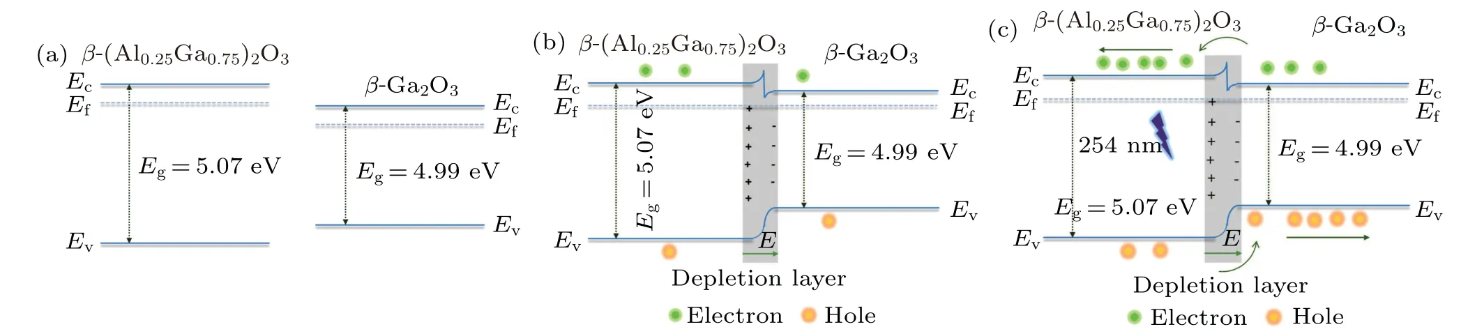
Fig.6. The energy band alignment of the β-(Al0.25Ga0.75)2O3/β-Ga2O3 heterojunction: (a)before contact,(b)after contact under dark state,(c)after contact under 254 nm illumination at 5 V.
4. Conclusion
In summary, we have compared the photodetection performances of two devices by growing anβ-(Al0.25Ga0.75)2O3passivation layer on the surface ofβ-Ga2O3films,and found that under the illumination with 254 nm light at bias 5 V,theβ-(Al0.25Ga0.75)2O3passivated devices show low dark current and high current on/off ratio compared to theβ-Ga2O3devices. The dark current is sharply reduced by about 50 times after passivation of theβ-Ga2O3surface,and the current on/off ratio increases by approximately 2 times. This is attributed to theβ-(Al0.25Ga0.75)2O3surface passivation,which reduces the surface trap state and the surface leakage current.Large and low defect densities in the epitaxial films are an influential factor. This result shows thatβ-(Al0.25Ga0.75)2O3exhibits high purity passivation effect and it has potential applications as a passivation material in the field of ultraviolet photoelectric detection.
Acknowledgements
Project supported by China Postdoctoral Science Foundation (Grant No. 042600055) and Research on Frontiers of Materials Science,Beijing Municipal Science and Technology Commission(Grant No.Z181100004418006).
猜你喜欢
杂志排行

Chinese Physics B的其它文章
- The coupled deep neural networks for coupling of the Stokes and Darcy–Forchheimer problems
- Anomalous diffusion in branched elliptical structure
- Inhibitory effect induced by fractional Gaussian noise in neuronal system
- Enhancement of electron–positron pairs in combined potential wells with linear chirp frequency
- Enhancement of charging performance of quantum battery via quantum coherence of bath
- Improving the teleportation of quantum Fisher information under non-Markovian environment