An insulated-gate bipolar transistor model based on the finite-volume charge method
2022-12-28ManhongZhang张满红andWanchenWu武万琛
Manhong Zhang(张满红) and Wanchen Wu(武万琛)
School of Electrical and Electronic Engineering,North China Electric Power University,Beijing 102206,China
Keywords: finite-volume charge method, IGBT device, lumped charge method, SPICE simulation, TCAD simulation
1. Introduction
Many models of PIN diodes and insulated-gate bipolar transistor(IGBT)devices have been proposed in the last several years to simulate power converter switching processes in circuits. Accurate and reliable device models can speed power circuit design and verification. So far, much effort has been made to develop and improve SPICE models of PIN diodes and IGBT devices from many aspects.[1–3]Hefner has developed a charge-control IGBT model based on the steadystate charge carrier distribution in the N−base region of a PIN diode.[4,5]Krauset al.developed another charge-control model based on a polynomial approximation of the partial time derivative of the charge carrier distribution.[6]The advantage of charge-control models is that only a few physical quantities are used to describe the behavior of power devices. The disadvantage is their lower accuracy due to the adoption of many simplifying approximations and the inability to adapt to different switching processes.[7]
Multiple-node methods such as the finite difference(FD)method,[8,9]the finite element (FEM) method[10]and the lumped charge(LC)method,[11,12]discretize the N−base region into several small parts in real space and solve the proper equations accurately. The Fourier series(FS)method is also a multiple-node method.[13,14]It expands the excess carrier density into several discrete components in wave vector space.These methods have a better tradeoff between accuracy and cost, and can be solved in circuit form either by MATLAB Simulink or SPICE simulators. Usually these multiple-node methods also adopt many approximations such as local quasineutrality and the one-dimensional(1D)approximation to describe the carrier dynamics in the undepleted N−base region.It is important to adopt more practical device conditions and more accurate approximations in device model development.
Luet al.included a two-dimensional (2D) correction to the boundary carrier density of the undepleted N−base region in the emitter–base junction side in IGBT devices using the FS method.[15]They obtained a better agreement between the simulation and experiments. Kanget al.implemented the FS method in a SPICE simulator to simulate a punch-through IGBT device with a N+buffer.[16]They made a diffusion approximation for the hole current in the N+buffer. As the ntype doping is only about 1016cm−3in the N+buffer, the electric field cannot be ignored and the drift current component can be comparable to the diffusion current component.We find this is the case through technology computer-aided design(TCAD)simulation. It is better if a model of an IGBT device has the same transport description in both the N−base region and the N+buffer. Due to the adoption of a limited number of wave vectors in the expansion,the FS method cannot describe the abrupt change of physical quantities very well.This method can be implemented in either MATLAB Simulink or SPICE simulators. In a Simulink simulation, complicated program charts need to be drawn.[14]In a SPICE simulation,it is necessary to make the summations over many wave vectors and to transform the carrier density from wave vector space to real space, resulting in very complicated equations. In these respects,the real space methods,such as FD and LC methods,have more advantages.On the other hand,FD and LC methods also share another problem. For example,in FD and LC methods,the spatial partial derivatives are approximated by the FD formula. During fast switching processes,the width of the depletion layer of the emitter–base pn junction changes, thus a moving grid is needed to discretize the base region. A direct adoption of the moving nodes to build the FD formula will cause an artificial loss of the carrier number during fast switching processes. Recently we proposed using the compensation electron and hole current components to conserve the carrier number in the FD method.[9]The compensation current components are proportional to the moving speed of the boundary of the undepleted N−base region and the average carrier density in this region. It is expected that such a correction is necessary in the LC method too. The FEM method does not use the FD replacement,but its equations are only valid under the condition of fixed boundaries of the undepleted N−base region,[10]so in this method it is also necessary to correct the effect of the moving boundaries.The FS method does not have this problem.[13,14]In this method, the boundary positions of the undepleted N−base region are determined by the boundary carrier densities through high-gain feedback controllers in SPICE simulations.[3]
The FD method is based on the ambipolar transport equation with a constant high injection carrier lifetime.[8,9]In contrast, the LC method is based on the drift–diffusion model.[11,12]It can use a density-dependent carrier lifetime,which is more accurate at a low injection level.[17]A further investigation of characteristics of the LC method is very useful. In the following we will analyze the main points and limitations of this method. We propose a new extension for this method, which we call the finite-volume charge (FVC)method.
2. Theoretical models
2.1. The FVC method versus the LC method
Figure 1(a) shows a punch-through IGBT structure. It has a thick N−base region with a donor doping level between 1013cm−3and 1014cm−3and a thin N+buffer layer with a donor doping level of about 1016cm−3. Without the N+buffer layer,the structure is called a non-punch-through type.As shown in Fig.1(b),an IGBT device is functionally equivalent to connecting the drain of an n-channel metal–oxide–semiconductor field-effect transistor(NMOSFET)to the base of a PNP bipolar transistor through a resistance-varying resistorRn. It is noted that the names of the IGBT collector and emitter terminals are opposite to those terminals of the PNP device. There are two pn junctions: the base–collector junction(denoted as J1)and the base–emitter junction(denoted as J2). In the on-state of the IGBT device, J1is forward biased and J2is reverse biased. Injecting a lot of electrons and holes into the N−base changesRn. Region I is the drain region of the NMOSFET and works as a junction field effect transistor(JFET). Electron and hole current components in this region are mostly 2D. In the base region (II) they are mostly along thex-direction apart from near the boundary between regions I and II.Currently most IGBT models make the 1D approximation in thex-direction. The drain terminal of the NMOSFET is assumed to be on the line ofx=W. The electron current through the channel region of the NMOSFET and region I is approximated using an empirical formula. Junction J2is assumed to extend to the whole range ofLalong they-direction.The electron and hole density are assumed to be zero at the depletion layer boundaryx=Wof the reverse-biased J2in Hefner’s IGBT model.[5]

Fig.1.(a)Schematic electron and hole current flows in a punch-through IGBT structure. (b)The equivalent circuit.


Fig.2. (a)The scheme of conventional[12] and(b)the improved lumped charge methods.[18] Only nodes in the N−base are shown.
Herep(x,t)is the hole density,which is approximately equal to the excess hole density,Eis the electric field,VTis the thermal voltage,Ais the cross-sectional area of the N−base andNBis the donor doping level in the base region. In order to use Eq.(1),Maet al.employed three discrete lumped-charge nodes in the undepleted N−base region.[11]In Fig.2(a),nodes 2, 3, and 4 are equally spaced with a neighboring distance ofd/2 in the undepleted N−base region of a non-punch-through IGBT structure.The geometry is rotated by 90◦with respect to that shown in Fig.1(a).The symboldhas the same meaning asWin Fig.1(a). There is also one more node across the depletion layer of the pn junction in each side: node 1 across J1on the left side and node 5 across J2on the right side. The hole carrier densities at the three nodes in the base region arep2,p3, andp4, respectively. The corresponding lumped charges at these three nodes are defined asqp2=qAdp2,qp3=qAdp3,andqp4=qAdp4. The electron and hole current components between nodes 2 and 3 are approximated as

These electron and hole currents are called current generators in SPICE circuits. In Eq. (2),QM,Tn23andTp23are defined asQM=qAdNB,Tn23=(d2/2)/(µnVT), andTp23=(d2/2)/(µpVT),respectively. In the LC method,Tn23andTp23are respectively called the electron and hole transit times between nodes 2 and 3. The voltages at nodes 2 and 3 arev2andv3with the definitionv23=v2−v3. Between node 3 and node 4, we can write similar equations for electron and hole current generators. The current continuity equation for charge conservation is given by

whereτBis the high-injection carrier lifetime in the base andQmis the total equilibrium minority hole density in the N−base region defined asQm=qAdn2i/NB. We useWdep1andWdep2to denote the depletion layer widths of J1and J2,respectively. The currents from Eq. (2) are assumed to be constant between adjacent nodes and not to be position dependent. No current continuity equation is set up for either of the carrier densitiesp2andp4.
Iannuzzoet al.have implemented the LC method in the form of a SPICE circuit.[12]The circuit shown in Fig.2(a)has a hole current branch and an electron current branch. For each space discretization node there is one hole circuit node and one electron circuit node at two sides of the current generatorIcont,kin the SPICE circuit. For voltage nodes,verticalIcont,kcurrent generators are replaced by vertical shorts to keep the vertically connected nodes at the same voltage. When the pn junction J1between nodes 1 and 2 is forward biased,the current generatorIcont,1is given by[18]

The first term describes the minority electron recombination in the left P+region in the collector. The second term describes carrier storage in the N−region related to the diffusion capacitance. It is expressed by[18]

This is a textbook equation for minority carrier injection in a long diode at a low injection level. HereQd2actually describes the hole injection into the N−region and the local charge neutrality means dQd2/dtalso gives the change of stored electrons in the N−region. For node 4,equations similar to Eqs.(4)and(5)can be written down with another term of carrier storageQd4. ChargesQd2,qp3, andQd4describe stored charges in the N−region and have a double counting problem. The minority carrier diffusion length in Eq.(5)may be replaced by a fitting parameter. The total stored charge is not accurately described in this approximation.
Duanet al.tried to improve Eq. (3) by adding another space discretization node(Fig.2(b))in the undepleted N−base region.[18]In this case,nodes 2,3,4,and 5 are equally spaced nodes with a distance ofd/3. Hered=Wis the width of the undepleted N−base region. There is also one more node across the pn junction depletion layer in each side: node 1 across J1on the left side and node 6 across J2on the right side. The hole densities at nodes 2 to 5 arep2,p3,p4, andp5,respectively. The current generatorsIn23/Ip23andIn34/Ip34are assumed at nodes 3 and 4, respectively. Duanet al.used three current continuity equations for regions 2 to 3, 3 to 4,and 4 to 5. The number of current continuity equations is still smaller than the total number of lumped charge nodes in the undepleted N−base region. Although they achieved very good agreement between experimental data and simulation results,[18]their improved LC method also introduced many different kinds of quantities and thus the method is complicated.
Our careful analysis of the LC method finds that it can be improved by the following points:
(i)Except for current generators from pn junctions at two boundaries,it is better to define and compute the electron and hole current generators only at the middle of two neighboring nodes.Figure 3(a)shows our discretization in the N−base of a non-punch-through IGBT device. Space discretization nodes are labelled asn1,n2,n3,n4and start fromn1in the N−base region. Nodesn2andn3are equivalent and their number can be easily increased if needed. In the following we assume the total number of nodes in the undepleted N−base isN. Noden1on the top starts from the collector side,the last nodenNat the bottom is at the emitter side. For each indexk, both the nodal voltagevkand the nodal carrier densitypkare define at nodenk. We define 2Nvariables as the basic quantities of an IGBT device. They are the nodal voltage differencevk+1–vk,the nodal carrier densitypkand the total collector currentIC.A detailed analysis shows that with a givenVGEthese basic quantities fully determine the state of the IGBT device. Functions of these basic quantities can be used to express other quantities such as the electron or hole current components in the N−region and the voltage drops across two pn junctions in an IGBT device;these are also called generators in our SPICE circuits.The current generator nodes are only atnI1,nI2,...,nIN+1. For example,for nodenI3between nodesn2andn3we have

Here ∆xis the distance betweenn2andn3. The electric fieldEand dp/dxare both computed as the central finite difference.The electron and hole current generatorsIn1andIp1at the positionn1−δ,InN, andIpNat the positionnN+δare computed from the device physics. The symboln1−δdenotes a position slightly above noden1and the symbolnN+δdenotes a position slightly below nodenN. The recombination currentIn1of minority electrons and the hole currentIp1in thep-type collector are expressed as


HereICis the total collector current.The equations forInNandIpNare complicated and will be given later.All current generators will form a SPICE current circuit in the SPICE simulation.
(ii) In contrast to the LC method, the carrier density at two boundary sidesp1andpNshould also fulfill the current continuity equations, so it is necessary to choose the control volumes properly to apply the current continuity equations.Figure 3(a)shows our choice of control volume.Its size at two boundaries is chosen as ∆x/2 and at all central places is chosen as the dimension of ∆x. The nodal carrier density and the control volume have a one-to-one correspondence. The following current continuity equations can be written for the boundary noden1(similarly fornN)andn2(similarly for other nodes):

HereIpn1n2andIpn2n3are computed at current generator nodesnI1andnI2, respectively.pm=n2i/NBis the equilibrium minority hole density in the N−base region.In the whole control volume, the total current is a constant, but the electron and hole current componentsInandIphave no definition except at the current generator nodes. In Fig. 3, all current generators are drawn in diamond symbols. Between the current generators expressed by diamond symbols dashed lines are plotted to indicate that only the total current is meaningful there. Eq.(8)will be converted into a SPICE circuit.

Fig. 3. The carrier density nodes, current generator nodes and control volumes in the FVC method: (a) a non-punch-through IGBT, (b) a punchthrough IGBT.
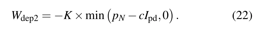
(iii)The collector–base pn junction J1is assumed to have the forward conduction, so the change in its depletion layer thickness will be ignored. The emitter–base pn junction J2is reverse biased and the change in its the depletion layer width is controlled by a high-gain feedback controller[3]

HereKis an empirical constant. The feedback keepspNto a small negative value. The change ofWdep2results in a change in the width of the undepleted N−base region. In the LC model,the reverse bias across J2is given by Eq.(10a)[12]

HereCJ2|1V=[qεSiNB/2(Vbi−VJ2)]1/2is the barrier capacitance of J2by settingVbi−VJ2=1 V.qpN ≡qdpNis the lumped charge at nodeNin the LC model. Equation (10a) is not a physical equation but an artificial feedback controller similar to Eq.(9). It can be written as the form of Eq.(10b)withKas an empirical constant.The feedback controllers in Eqs.(9)and(10c)have been used in the FD and FS simulation approaches of PIN diodes before.[9,14]Equations(9)and(10)are equivalent to each other. Other forms of feedback controller are also possible.
(iv)Figure 3(b)shows a punch-through IGBT device with a N+buffer with a doping levelNH,a widthWHand a high injection carrier lifetimeτH.At noden2,at the interface between the N+buffer and the N−base, the voltagev2is continuous,but the carrier density is not continuous. Therefore, noden2for the carrier density is split into two nodes:n2hin the N+buffer side andn2lin the N−base side. Nodesn2handn2lcan also be expressed asn2+δandn2−δ.
The carrier densities at these two nodes connected by

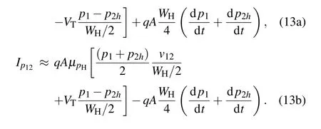
In deriving these equations,the carrier number in the N+buffer is assumed to beAWH(p1+p2h)/2. Current generators in Eqs.(6)and(13)are assumed to be between nodesn1andn2,so the total current equals the sum of electron and hole current generators in Eqs.(12)or(13)from nodesn1ton2. This point is useful for establishing the SPICE simulation circuit.With Eq. (13), the charge current continuity equation can be written as

HereIp23andIn23are defined at the middle of noden2landn3.pmH=n2i/NHis the equilibrium minority hole density in the N+buffer.τH=τB=τp+τn=13 µs is chosen as the high-injection lifetime in both the N−base and the N+buffer.The definitions of other current generators follow Eq.(6)and Fig. 3(a). Other choices of control volume forn1andn2are also possible. For example,if choosing Eq.(12)as the current generator in the N+buffer one can take the top half of the N+buffer as the control volume forn1and the bottom half of the N+buffer plus a small part of the N−base region with a dimension of ∆x/2 below noden2las the control volume forn2.The resultant current continuity equation for noden2will be slightly complicated,but our tests show the results are almost the same.
(v) Finally, we also include the compensation electron and hole current corrections at nodeNdue to the change ofWdep2in transient processes. Such corrections are important for fast switching PIN diodes.
With the above improvements, the new scheme can be thought as an extension of the LC method or better as the FVC method. Carrier conservation is fulfilled much better by the present choice of the positions of current generators and the control volumes. In addition, only the total collector current,the nodal carrier density and voltage are chosen as basic quantities in the new scheme. In the following we will compare the TCAD simulations of an IGBT device with SPICE simulations based on the new method.
2.2. SPICE circuit implementation of the FVC method
Figure 4 shows our SPICE current circuit implementation of the FVC method in a punch-through IGBT.EjandEdsare two voltage generators across the depletion layers of the collector–base and emitter–base pn junctions,respectively.Ejis connected between node C andn1givingEj=v1−vC,Edsis connected betweennN=dand nodeE=sgivingEds=vd−vE. Here d and s are the drain and source terminals of the NMOSFET in the IGBT device. The symboldis the width of the undepleted N−base region only in the LC method. The electron and hole current throughEjareIn1andIp1.Ejis given by the following equation:

The nodes equivalent ton3can be increased.As discussed above, the total currentICis constant between two neighboring voltage nodes. It is expressed as the sum of the local electron and hole current generators. Each voltage node is also connected to the ground through a large resistor,for example,100 MΩ.This makes every voltage node have a DC pass to the ground. The definition of the voltage-controlled sourceVdepis the same as in the LC method.[18]
The electron current at noded=nNis

Herexdepis the zero-bias depletion layer width of the emitter–base pn junction J2.Imos(Vgs,Vds) is the DC channel current in the NMOSFET. Figure 1(a) shows schematically the electron and hole current flows in a 2D TCAD IGBT structure. In this figure, we haveW −W0=xdep0+Wdep2.Ais the crosssectional area of an IGBT cell in they–zplane andAgdis the area of the gate overlapping with the drain. In Fig.4 the current flow is approximated as a 1D one. The third term ofIndin Eq.(16)is a displacement current in the drain and the capacitanceCgdis not a constant but depends onVdg. In the real implementation,this term is described by the voltage-controlled voltage sourceVdepconnected in series with a constant gate oxide-related capacitanceCoxdin the LC method. The fourth term ofIndis added by us.[9]It is due to the adoption of the moving uniform nodes indexed fromn3tonNto describe the effect of the moving boundary of the depletion layer atx=W.The symbolpdenotes the average carrier density in the undepleted N−base region. This term may be small for the slow change of dWdep2/dtin IGBT devices due to the large gaterelated capacitance, but cannot be ignored in fast-switching PIN diodes.
Near the linex=Win Fig. 1(a), the current flow has a 2D property. A small part of the hole current flows from the bottom vertically through the depletion layer of the emitter–base pn junction J2in the left side. We will ignore this small hole current component to derive the 2D correction and assume that the hole current flows from the bottom region II to the top direction and makes a right turn nearx=Winto region I, where it turns left to the P-well. In Fig. 1(a), the physical property on the line ofx=Wis not uniform. However, in Fig.4 this line is approximated as the drain terminald. WhenVCEis small, the depletion layer of the emitter–base pn junction J2is only distributed in the left side, and whenVCEis high enough and the current is low, the depletion layer starts to extend to the full region under the gate. The 2D nature is clearly visible in the emitter side. In an IGBT model,Vdsis defined by the bias across the emitter–base pn junction J2. It is not equal to the usual drain–source voltage difference of the NMOSEFT.As the other part ofVdsdrops in region I shown in Fig.1(a),which works as a JFET,the value ofVdsis easily extracted from the potential distribution in the depletion layer of the emitter–base pn junction J2nearx=Wat the left boundary from TCAD simulation. Thus,we can extractImosversusVdsfrom the DC voltage sweep of the TCAD simulation. The following behavior model for the NMOSFET channel current is used forVgs=VGE>Vth:


The IGBT device is really a multi-dimensional device.However, the existing SPICE IGBT models are still 1D ones with a proper inclusion of some 2D effects. We still follow this direction to set up our FVC SPICE IGBT model. Let us make the 1D approximation and assume the depletion layer of the emitter–base pn junction J2is uniformly distributed along they-axis.Ipdis the total hole current atx=WthroughEds.Here we do not add the effect ofIndin the definition ofNeff.WhenVdsis small, only a very small fraction of hole current passes through the depletion layer to contribute toNeffin the TCAD simulation. However,this correction is comparable toNBand cannot be ignored. WhenVdsis high,the electron current will pass though the depletion layer, but the NMOSFET works in saturation and the error ofNeffdoes not affectImostoo much.It is noted thatEdsis a voltage-controlled voltage source ifWdep2is taken as a generalized voltage signal andVdsis the voltage difference between nodes d and s. Finally, the current continuity equation, for example (14c), is converted into a SPICE circuit by scaling the hole density ~pi=pi/N0withN0=1×1016cm−3·V−1, and making the time-to-resistance transformationRB=τB/C0withC0=1×10−6F:
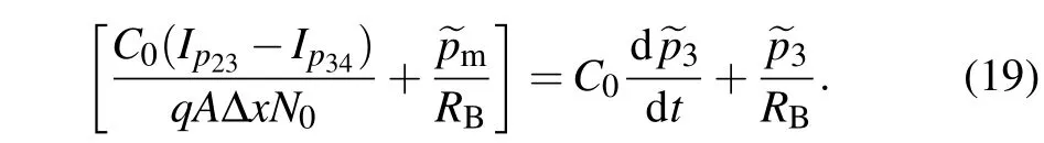
The term in the left of Eq. (22) is just another generalized current generator. Similar conversions can be done for other current continuity equations. For an IGBT device above the threshold,our simulation shows that the high-injection approximation used in Eqs.(14)and(22)is good enough. However, the literature results and our simulation show that for a PIN diode switching between a forward-biased state and a reverse-biased state, the use of a density-dependent lifetime covers both the low- and high-injection regions, and gives a more accurate current.[17]
The width of the undepleted N−base is given by the following equation in the FVC method:

Note that this width is expressed bydin the LC method and byWin the FVC method.
In the 1D Hefner IGBT model,[4,5]the electron or hole density atx=Wis zero. In the 2D TCAD IGBT structure shown in Fig.1(a),the average carrier density over they-axis atx=Wis not zero; this results in a higher collector current at the same terminal bias. Several papers have investigated 2D effects. Luet al.found that the average hole densityplmover thelmedge on the right-hand side of Fig.1(a)is approximately proportional to the total hole currentIpWatx=W. They further assumed the same relation held atx=Wbetween the average hole carrier densitypNover theL-dimension and the hole currentIpd. In Fig.1(a),Lis the dimension of an IGBT cell on they-axis. We also definePwas the average hole density over theL-dimension atx=Wandaiasai=lm/L. We will test this assumption using the data from the TCAD simulation and adopt it in our SPICE simulation. The two relations are given as follows:
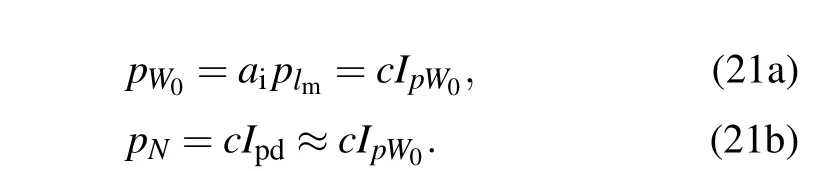
Herecis a parameter. The approximationIpd≈IpWis also adopted in Eq. (21b). With Eq. (21), equation (9) is changed into[15]
This can also be converted into a SPICE circuit by takingWdep2as a generalized voltage.

Fig. 4. Schematic picture of the SPICE current circuit implementation of a punch-through IGBT in the FVC method.
A theoretical formula for parametercis given as[15]
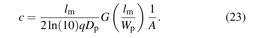
HereDpis the hole diffusion coefficient. The functionG(x)is defined in Lu’s paper.[15]The areaAis given asA=LLZ.Although the parameterlmis bias-dependent it was taken as a constant in Lu’s paper.[15]
3. Results and discussion
In this paper, Sentaurus TCAD software and the LTSPICE simulator are used to do simulations. Two node numbers ofN=11 andN=4 are compared. All parameters used in this paper are presented in Table 1.
Based on Fig. 1(a), we extractVdsfrom the TCAD simulated potential, electron and hole distributions across the emitter–base pn junction J2in a cut line aty= 9 µm. In our TCAD IGBT cell structure, near the left boundary aty=10.25 µm, junction J2is almost uniform and can be approximated as 1D in thex-direction. Then we can formImos–Vdscurves. From these curves, we can extract the MOSFET parameters. However, the emitter–base pn junction J2is not an abrupt junction,so a direct use of the textbook pn junction equations will cause errors of parameters. When a MOSFET works in saturation, it is well known that the total anode currentICEis proportional to the electron currentImos. In this case,we have


Table 1. Parameters of the TCAD IGBT and circuit.

Fig.5. The dependence of parameter c on Vds extracted from TCAD simulation at x=W0 and x=W. The spread of the data is partly due to a weak VGE dependence.
Here theλ-dependence inImosis ignored. From TCAD simulatedICE–VGEcurves at oneVCEvalue,Vthandθcan be extracted very accurately.
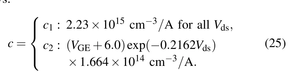
We then extract the parametercdefined in Eq.(21)from TCAD simulation. Figure 5 shows their values versusVdsextracted atx=W0andx=W. The data are not on a single curve due to a weakVGEdependence. The values of parametercextracted atx=W0andx=Walmost overlap with each other. The value ofcis 2.5×1015cm−3·A−1atVds=1 V,and decreases with increasingVds. In order to make SPICE simulation possible, two kinds of expressions forchave been tested in this paper: A constant value and a biasdependent expression. They are denoted as choicec1andc2,respectively. Choicec1was used by Luet al.[15],with whichc=2.89×1015cm−3·A−1can be computed from Eq. (23).Then this value is adjusted slightly to give the SPICE simulation a better agreement with our TCAD simulation data. Finally,we takec=2.23×1015cm−3·A−1in choicec1. Choicec2is obtained by fitting the data of Fig.5 to a proper analytical formula. The two choices of parametercare summarized as follows:
Figures 6(a) and 6(b) show the collector currentICversusVCEwithout and with the 2D correction,respectively. The results demonstrate the importance of the 2D correction. In Fig. 6(a),ICvalues are very different forN=11 andN=4.With choicec1in Fig.6(b),ICvalues forN=11 andN=4 are close to each other. AdoptingN=4 gives higherICvalues in the linear region due to the error in computing the electric field−∆v/∆xand the carrier density gradient ∆p/∆x. In a transient process,the charge profile changes very fast in space so a larger node number will give a better accuracy. Figure 6(b)shows that forVGE≤10 V,the choicec2of parametercgives betterICcurrent curves,and forVGE=15 V,the simple linear dependence onVGEin choicec2is not enough. The choicec1for parameterccan easily achieve convergence in the SPICE simulation under different conditions. However, the data for choicec2for parametercare obtained by converting the results of DC sweeps under a constantVCEcondition. A DC sweep under a constantVGEcondition does not converge for choicec2of parameterc. This indicates that there is still an incompatibility in incorporating the 2D correction in the simple 1D approximation. In the following we will take choicec1for parametercto perform the transient SPICE simulation. Finally, we have done a TCAD mixed-circuit transient simulation. Figure 7 shows the circuit used for the TCAD mixed-circuit simulation and FVC-based SPICE simulation.Figure 8 compares theIC,VGEandVCEwaveforms simulated using the TCAD mixed-circuit simulation and the FVC-based SPICE simulation. The nominal drain–gate overlap area isAgd=lmLZ. To get a better agreement between the TCAD mixed-circuit simulation and the FVC-based SPICE simulation,a smallerAgd=0.6lmLZis used in the SPICE simulation.Checking the electron density under the gate at a switching time of 2.7µs from TCAD simulation shows that only a part of arealmLZcontributes to the capacitanceCdg.The agreement between TCAD simulation and theN=11 SPICE simulation is very good. TheN=4 SPICE simulation is less accurate than theN=11 one.
The above results demonstrate the effectiveness of our FVC method and the necessity for 2D corrections to the SPICE simulations of IGBT devices. The nonconvergence of the DC sweep ofVCEunder constantVGEwith choicec2for parametercshows that the implementations of 2D corrections at the present stage are not perfect and can be improved further. It is desirable to give up the simple 1D approximation and develop an IGBT model based on multi-region carrier distributions. Shenget al.and Feileret al.have done pioneering work in this direction.[19,20]The N−base region is further divided into left and right regions. However,in Sheng’s work,the regional carrier density distributions do not consider the mutual charge transfer and are not used to derive the final collector current either.[19]In Feiler’s model,charge transfer is allowed between different regions but carrier recombination is completely ignored.[20]We hope to develop a better IGBT model in the future to account for the 2D effects more accurately and then use it to do SPICE simulations.

Fig.8. Comparison of IC,VGE, and VCE waveforms simulated using TCAD mixed-circuit simulation and FVC-based SPICE simulation.

Fig.6. The collector current IC versus VCE at different VGE: (a)without 2D correction,(b)with 2D correction using two choices for parameter c.
4. Conclusion
In summary,a finite-volume charge method has been proposed to simulate PIN diodes and IGBT devices using SPICE simulators by extending the lumped-charge method. The new method assumes local quasi-neutrality in the undepleted N−base region and uses the total collector current, the nodal hole carrier density and voltage only as the basic quantities.Besides the carrier density nodes and the voltage nodes, the SPICE circuit also defines all current generator nodes at clear positions. It uses central finite difference to approximate electron and hole current generators, and sets up the current continuity equation in a control volume for every carrier density node in the undepleted N−base region. We use this method to simulate a punch-through IGBT device in the LTSPICE simulator. The results are in very good agreement with TCAD simulations. We have compared two kinds of 2D correction formulae for the hole boundary density in the emitter–base side and demonstrated the importance of 2D correction.
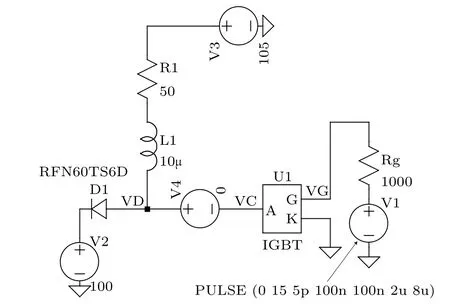
Fig.7. The circuit used for TCAD mixed-circuit simulation and FVC-based SPICE simulation.
杂志排行

Chinese Physics B的其它文章
- Editorial:Celebrating the 30 Wonderful Year Journey of Chinese Physics B
- Attosecond spectroscopy for filming the ultrafast movies of atoms,molecules and solids
- Advances of phononics in 20122022
- A sport and a pastime: Model design and computation in quantum many-body systems
- Molecular beam epitaxy growth of quantum devices
- Single-molecular methodologies for the physical biology of protein machines