Molecular beam epitaxy growth of quantum devices
2022-12-28KeHe何珂
Ke He(何珂)
1State Key Laboratory of Low-Dimensional Quantum Physics,Department of Physics,Tsinghua University,Beijing 100084,China
2Frontier Science Center for Quantum Information,Beijing 100084,China
3Beijing Institute of Quantum Information Science,Beijing 100193,China
Keywords: molecular beam epitaxy,fabrication,ultrahigh vacuum,quantum computation
“The interface is the device”. The manifesto by Herbert Kroemer,the 2000 Nobel Laureate in Physics,incisively summarizes the central role of interfaces in the function and performance of electronic devices.[1]The saying is even truer for devices based on low-dimensional or topological quantum materials whose properties are often sensitive to a few atomic layers around the surfaces and interfaces.[2–5]Such delicate“quantum devices” call for fabrication techniques capable of achieving atomically clean,abrupt and flat interfaces in a wellcontrolled manner. It is obviously beyond the scope of traditional fabrication processes under the low vacuum,ambient air or solution circumstance.
Molecular beam epitaxy (MBE) is a preparation method that can provide arguably the best interface condition and controllability with the ultrahigh vacuum (UHV) environment,high-purity evaporation sources, slow growing rate, and finetunable growth parameters.[6]The standard MBE technique is usually used to grow thin films and vertical heterostructures. Some in-plane nano-structures can also be prepared by MBE,[7,8]but not in a so well-controlled way as conventional photo or electron beam lithography. The “clean” samples grown by MBE have to experience“dirty”fabrication processes to be made into devices. The uncontrolled surfaces and interfaces produced in these processes can significantly modify the performance of the devices, especially those made of surface/interface-sensitive quantum materials. It is highly desirable that the extremely fragile devices composed of quantum materials are directly grown by MBE and then encapsulated in the UHV environment so that their genuine properties could be preserved.
In the past years, encouraging experimental progress has been made in techniques on direct MBE growth of inplane nanostructures and devices,[9–18]largely driven by the need for scalable fabrication of high-quality semiconductor–superconductor hybrid nanowire networks to realize topological quantum computing.[19–25]The basic idea is to perform MBE growth on substrates pre-patterned by usual fabrication techniques. By choosing different structures on the substrates and controlling the MBE growth parameters, one can grow various epitaxial in-plane nano-structures and heterostructures in a UHV chamber. Since the“dirty”fabrication processes are shifted either before or after the sample growth, their influences can be minimized by proper substrate cleaning and sample capping, while the crucial interface regions are prepared by MBE in the UHV environment. Below, I will introduce several such techniques developed in recent years.
The selective area growth (SAG) technique can be used to grow in-plane epitaxial nano-structures,such as nanowires,nanowire networks, and nanodot arrays. The substrate for SAG is first capped by a dielectric film (mask). With electron beam lithography (EBL) or photolithography, openings are fabricated on the mask where the substrate surface is exposed(see the schematic procedure shown in Fig.1(a)). After proper cleaning,the patterned substrate is loaded into the UHV chamber for MBE growth. Dielectric films are usually naturally surface-passivated, hosting fewer dangling bonds at the surface than semiconductors. Therefore,the atoms evaporated onto the pre-patterned substrate move faster on the mask surface than on the bare substrate surface, which leads to higher nucleation density in the latter. By controlling the substrate temperature and evaporation flux, it is possible to find a parameter window in which the evaporated material only grows on the bare substrate surface at the openings (Figs. 2(b) and 2(c)). This way, one can grow intended nanostructures with MBE by fabricating the openings with needed shapes.

Fig. 1. (a) Schematic procedure of a typical fabricating process of patterned substrates for selective area growth (SAG). (b) In-plane InSb nanowire network grown on InP substrate with Si3N4 mask by SAG, cited from Ref. [15]. (c) In-plane PbTe nanowire and other structures grown on CdTe substrate with Al2O3 mask by SAG,cited from Ref.[29].
The SAG technique first appeared as early as 1960s[26]and has been used to prepare photonic devices.[27]In recent years, it has drawn much attention as a powerful fabrication tool to realize scalable topological quantum computing — a fundamental solution to the fault-tolerant quantum computing.[19–25]A semiconductor–superconductor hybrid nanowire under magnetic field can host Majorana zero modes (MZMs) at their ends.[19,20]The MZMs in a network composed of several such hybrid nanowires can be encoded into topological quantum qubits and manipulated to realize topological quantum gates(known as braiding). Selective area growth is an ideal method to directly prepare in-plane singlecrystal nanowire networks, avoiding the connection problem between nanowires.There have been several works on SAG of InAs and InSb nanowires, with the reported mobility as high as∼25000 cm2/V·s.[9–16]The SAG nanowires have been considered as one of the most promising approaches to a scalable topological quantum computer.
Actually, nanowires are expected to exhibit even higher crystalline quality than macroscopic bulk crystals or thin films due to the lower density of defects promised by the finite-size effect (similar to single crystal whiskers). However, the quality of InAs/InSb nanowires is limited by the unsatisfactory substrates. The ideal substrate used in SAG should have good lattice match and little interdiffusion with the nanowires. Unfortunately, one cannot find substrates that have both the well-matched lattice constant and negligible interdiffusion(at the growth temperature of the nanowires)with InAs or InSb. The big lattice mismatch with the commonly used substrates such as InP leads to strain or twin boundaries in the nanowires.[11–13,16]Although one can obtain single crystal nanowires by realizing a single nucleation site for one nanowire with fine-tuned growth parameters,[15]the crystalline dislocations due to the lattice mismatch still exist at the interface to the substrate which may keep the sample quality from further improving.
The problem is naturally solved in another candidate Majorana nanowire system: PbTe grown on CdTe.[28–30]PbTe and CdTe are nearly perfectly lattice-matched, but their bulk crystalline structures are distinct, rocksalt for the former and zincblende for the latter, which minimizes the interdiffusion between the two materials. As a result,PbTe nanowires grown on CdTe substrates experience little strain or interdiffusion.Such nearly free-standing nanowires provide an ideal platform for the studies of MZMs and topological quantum computation.
Another quite interesting UHV nanostructure fabrication technique, similar to SAG, has recently been applied to prepare Si:P quantum dot arrays on silicon for quantum simulation.[31,32]A silicon substrate is first passivated with hydrogen which acts as a mask layer.In UHV,the hydrogen layer is selectively desorbed by a scanning tunneling microscope(STM) tip. After that, the substrate is exposed to phosphine(PH3) gas, and the PH3molecules are only incorporated into the bare surface without the hydrogen layer.The resulting Si:P quantum dots are then capped by an MBE-grown Si layer for further device fabrications. Thanks to the high-accuracy positioning of the STM tip,the technique allows for fabrication of sub-10 nm structures,breaking through the limit of EBL.
In-plane heterostructures such as superconducting Josephson junctions can be fabricated with MBE growth through shadow masks.[15,16,29]It guarantees the formation of atomically clean and flat semiconductor–superconductor interfaces, which is crucial for the topological superconducting states residing there. To obtain structures of sub-micrometer size, the shadow masks should be fabricated on the substrate(on-chip) to make sure that the mask–substrate distance is enough close and well-controlled. The substrate temperature should be kept as low as possible because the diffusion of the evaporated atoms on the substrate surface will blur the edge of the deposited film. Actually, the method is usually used to prepare superconductors such as Al and Pb which grow in a two-dimensional manner only on substrates kept at a low temperature(say,<150 K).
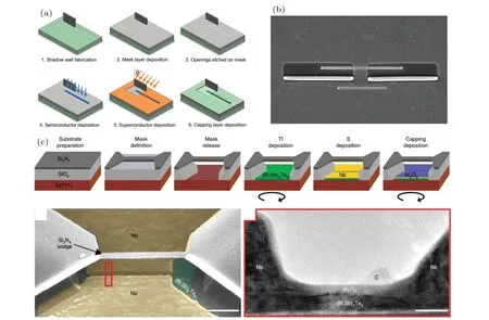
Fig.2. (a)Schematic fabrication procedure of semiconductor nanowire–superconductor in-plane heterostructures by combining selective area growth (SAG) and shadow wall growth, cited from Ref. [29]. (b) PbTe–Pb heterostructures prepared by the procedure shown in (a). (c)Schematic fabrication procedure (up) and an actual device (down) of a superconducting Josephson junction on a topological insulator film prepared by combining SAG and shadow mask growth,cited from Ref.[17].
Similar shadow evaporation methods have been used in fabricating Josephson junctions in superconducting qubit devices by using organic electron beam- or photo-resists as the masks.[33]However, the organic resists are not compatible with the UHV environment for MBE growth, especially considering the strict substrate cleaning processes such as high temperature annealing and ion sputtering.
Therefore,inorganic materials such as Si3N4deposited by plasma-enhanced chemical vapor deposition(PECVD)or metalorganic vapor-phase epitaxy (MOVPE) were used to make on-chip shadow masks for MBE growth. The shadow masks usually have relatively simple wall-like structures (shadow walls)to avoid influencing substrate cleaning. A simpler way to fabricate shadow walls is by using inorganic negative electron beam resist hydrogen silses quioxane (HSQ) which is converted into SiOxafter electron beam exposure, compatible with the UHV environment after proper cleaning and outgassing.[29]By evaporating a material with a certain incidental angle, the film is only grown on the area outside the shadows of the walls. Combining the SAG and shadow wall growth,one can directly prepare in-plane semiconductor–superconductor heterostructures with MBE and protect them by a capping layer, all in one UHV chamber[17,29](see the schematic procedure in Figs. 2(a) and 2(b)). More delicate mask structures including suspended bridges have also been developed, extending the scope of the technique[17,34](Fig. 2(c)). Further development in this direction may eventually lead to MBE growth of Josephson junctions for superconducting qubit chips.
These UHV compatible fabrication techniques based on MBE growth on pre-patterned substrates have shown great power in making high-quality devices in a scalable way for solid state quantum computing,especially in achieving nearly ideal interface conditions. On the other hand, as MBE-based techniques, they rely on careful control of the growth kinetics, and the growth conditions and parameters usually vary from materials to materials. Actually, the selective nucleation required by the SAG and the small diffusion length required by the shadow mask growth greatly narrow the parameter window to grow single crystalline nanostructures, making the growth condition optimization more challenging than usual MBE.Therefore,the MBE-based fabrication techniques are not so flexible as conventional ones and have not been so widely used. Rather, for devices made up of given materials,one can develop the specific MBE-based fabrication techniques for them to push the device quality to a higher level.Accumulation of various MBE-based fabrication techniques for different systems may eventually lead to a new-concept chip-making technology based on novel, though usually extremely fragile and surface/interface-sensitive,quantum materials.
Acknowledgement
Project supported by the National Natural Science Foundation of China(Grant No.92065206).
杂志排行

Chinese Physics B的其它文章
- Editorial:Celebrating the 30 Wonderful Year Journey of Chinese Physics B
- Attosecond spectroscopy for filming the ultrafast movies of atoms,molecules and solids
- Advances of phononics in 20122022
- A sport and a pastime: Model design and computation in quantum many-body systems
- Single-molecular methodologies for the physical biology of protein machines
- Research progress of Pt and Pt-based cathode electrocatalysts for proton-exchange membrane fuel cells