Temperature dependence of spin pumping in YIG/NiO(x)/W multilayer
2022-12-28LijunNi倪丽君WenqiangWang王文强LichuanJin金立川JiandongYe叶建东HeheGong巩贺贺XiangZhan战翔ZhendongChen陈振东LonglongZhang张龙龙XingzeDai代兴泽YaoLi黎遥RongZhang张荣YiYang杨燚HuaiwuZhang张怀武RonghuaLiu刘荣华LinaChen陈丽娜andYongbingXu徐永兵
Lijun Ni(倪丽君) Wenqiang Wang(王文强) Lichuan Jin(金立川) Jiandong Ye(叶建东)Hehe Gong(巩贺贺) Xiang Zhan(战翔) Zhendong Chen(陈振东) Longlong Zhang(张龙龙)Xingze Dai(代兴泽) Yao Li(黎遥) Rong Zhang(张荣) Yi Yang(杨燚) Huaiwu Zhang(张怀武)Ronghua Liu(刘荣华) Lina Chen(陈丽娜) and Yongbing Xu(徐永兵)
1Jiangsu Provincial Key Laboratory of Advanced Photonic and Electronic Materials,School of Electronic Science and Engineering,Nanjing University,Nanjing 210093,China
2State Key Laboratory of Electronic Thin Films and Integrated Devices,University of Electronic Science and Technology of China,Chengdu 610054,China 3Jiangsu Provincial Key Laboratory for Nanotechnology,School of Physics,Nanjing University,Nanjing 210093,China
4Jiangsu Key Laboratory of Opto-Electronic Technology,Center for Quantum Transport and Thermal Energy Science,School of Physics and Technology,Nanjing Normal University,Nanjing 210023,China
5School of Science,Nanjing University of Posts and Telecommunications,Nanjing 210023,China
6York–Nanjing Joint Centre for Spintronics and NanoEngineering,Department of Electronic Engineering,University of York,York YO10 5DD,United Kingdom
Keywords: spin pumping effect,spin transport,charge current Ic,linewidth ∆H,temperature dependence
With the development of spintronics, the generation and detection of spin current have become a topic of concern.Meanwhile, the controllable modulation of the spin transport of electrons is also central to fabricating robust spintronics devices.[1–5]Spin transport in ferromagnetic (FM) and nonmagnetic materials (NM) has been extensively studied. Pure spin current can be pumped from FMs into NMs by ferromagnetic resonance (FMR) spin pumping[6,7]or a thermal gradient.[8,9]Furthermore, the pure spin current can be converted into the charge currentIcby the ISHE due to bulk and interfacial spin–orbit coupling at the NM and FM/NM interface,[10]thereby realizing the electrical detection of pure spin current. So, the effective modulation of spin current injection and the spin transport plays an important role for the impact onIcin FM/NM heterostructures.
Recently, spin current studies, especially spin transport,have been expanded into the antiferromagnetic (AF) materials, e.g., NiO, IrMn, and Fe2O3.[11–15]For instance, NiO is a well-known AF insulator with a bulk N´eel temperature ofTN=525 K.[16]And the characteristic frequency of AF NiO is up to 1 THz in magnetic resonance measurements,which is attractive for developing THz devices.[17]Surprisingly,the unexpected enhancement of spin transport via inserting thin AF NiO between an FM(such as YIG)and Pt was discovered in FMR spin pumping and spin Seebeck experiments.[9,12,18,19]The spin transport in the AFs is optimal at a temperature near the AF Ne´el temperatureTN, suggesting that the spin transport through the AF insulators is related to AF magnons and strong spin fluctuations nearTN.[7,9]In addition, Hammelet al.[20]found that the transport efficiency of spin currentJswas reduced at room temperature, when a Cu layer was inserted between YIG and Pt in FMR spin pumping experiment. While the insertion of a similar Cu interlayer between YIG and W improves the spin currentJsinjection into W.Therefore, it is interesting how spin transport is affected if the NiO interlayer is inserted between YIG and W.In fact,Chienet al. have reported that 1-nm thin NiO suppressed the spin current pumped into W from YIG in the Seebeck effect experiment only measured at room temperature.[9]Hence, it is necessary to systematically explore the effect of temperature on spin transport between YIG and W with different NiO interlayer thickness.However,very few studies have been reported on this topic so far.
So, we systematically explore the effect of temperature on spin transport between YIG and W with different NiO interlayer thicknesses. We chose YIG/NiO (tNiO)/W (6 nm)(tNiO=0 nm, 1 nm, 2 nm, and 10 nm) stacked structure and focused on the FMR spin-pumping-induced charge currentIcover a wide temperature range (30–300 K). The transmitted spin current detected by ISHE in the W had a maximum near theTNof the AF NiO layers, consistent with the previous reports in the YIG/NiO/Pt system. On the contrary, we found that 1 nm thick NiO is enough to significantly suppress spin transport between YIG and W by varying NiO thickness, indicating that interfaces in YIG/NiO/W heterostructures play a vital role in the spin transmission except for magnetic fluctuation of the AF NiO spacer.
The 0.9-µm thick YIG films were grown on Gd3Ga5O12(GGG, (111)) substrates by liquid-phase epitaxy. The YIG samples were degreased via ultrasonic bathing in acetone and ethyl alcohol for 12 min and cleaned by deionized water, before being placed into the deposition chamber. Then,we used ultrahigh vacuum magnetron sputtering with a base pressure of 3×10⁻⁸Torr to fabricate the YIG(0.9µm)/NiO(tNiO)/W(6 nm) (tNiO= 0 nm, 1 nm, 2 nm, and 10 nm) samples at room temperature. The reactive (Ar+O2) pressure for NiO deposition was 4.5×10⁻³Torr. And the working Ar pressure was 5×10⁻³Torr for W deposition. Finally,all samples were patterned into a 4.0-mm long and 0.5-mm wide small rectangular bar by combining optical lithography and ion Ar+plasma etching. The FMR spin pumping measurements of YIG(0.9µm)/NiO(tNiO)/W(6 nm)(tNiO=0 nm,1 nm,2 nm,and 10 nm) samples were performed by using the coplanar waveguides (CPW) method over the temperature range from 300 K to 30 K, and the microwave frequency (f) and power(Prf) were set to be 9 GHz and 20 dBm, respectively. As illustrated in the schematic diagrams shown in Fig. 1(a), the external bias magnetic fieldHwas applied along thex-axis,and voltage measurements were performed along they-axis.At YIG resonance, the precessing YIG magnetization excites the AF moments at YIG/NiO interface. The AF magnons or fluctuations in NiO carry the angular momentum (a vertical spin currentJs) through the NiO thickness to the NiO/W interface,where the angular momentum is transferred across the NiO/W interface to the conduction electrons in the metal layer W along thez-axis with the spin polarization along thex-axis.Then,Jsin W can be converted to a charge currentIcvia ISHE.
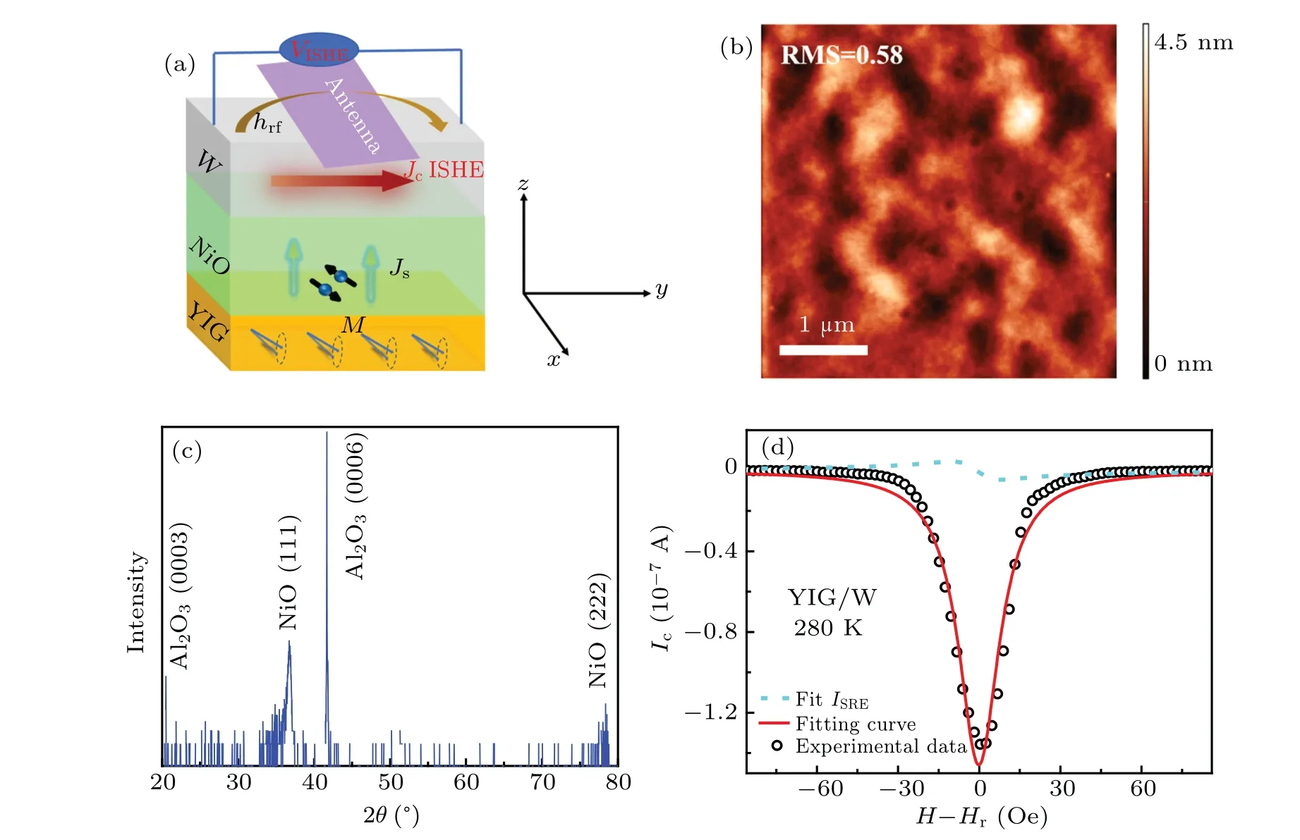
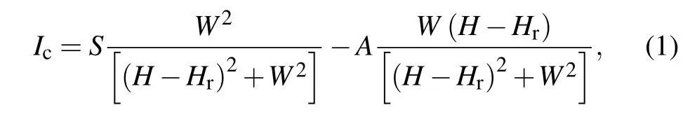
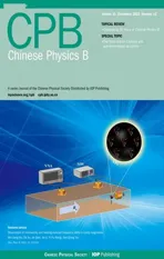
Fig.1. (a)Schematic of the spin pumping and ISHE measurement with in-plane field H,(b)the atomic force microscopy images of the 0.9-µm bare YIG over an area of 4µm×4µm,(c)XRD spectrum of a 400 nm-NiO film,(d)fitting of the experimental data of Ic and the antisymmetric component for YIG/W at 280 K.
Atomic force microscopy (AFM) measurement shown in Fig. 1(b) reveals a root-mean-square (RMS) roughness of 0.58 nm for bare YIG, demonstrating the smooth surface of YIG film. High-resolution x-ray diffraction(XRD)scan of the 400-nm thick NiO film deposited on thec-plane sapphire substrates is presented in Fig.1(c). Only(111)and(222)peaks of NiO film are detected,indicating that the NiO films are of high quality with a preferred orientation along〈111〉. As plotted in Fig.1(d),we fit a typical charge currentIccurve of the YIG/W sample at 280 K by the expression as follows:[19]
whereSis the symmetric part of the voltage amplitude,which corresponds mainly to the voltage coming from ISHE, andAis the antisymmetric part, which originates from spin rectification effect (SRE), respectively. TheWis half of the resonance linewidth ∆H. TheHrrepresents the resonance field.The asymmetric signalISREis negligible, and the symmetric Lorentzian shape can mainly fit the experimentalIccurve.

Fig.2. (a)The Ic vs. H −Hr spectra derived from FMR spin pumping voltage measurements for the YIG/NiO(tNiO)/W(6 nm)samples with tNiO of 0 nm,1 nm, 2 nm, and 10 nm. The inset in (a) only shows the magnetic field dependence of the Ic for the sample with tNiO =10 nm.(b)At T =280 K and f =9 GHz,normalized charge current Ic/Ic0 as a function of the NiO thickness.
Figure 2(a) shows that the charge currentIc(Ic0) vs.H −Hr(Hris the resonance field of YIG)spectra for YIG/NiO(tNiO)/W (tNiO=0 nm, 1 nm, 2 nm, and 10 nm) samples atT=280 K,andf=9 GHz. TheIc0of the YIG/W sample at the FMR point is 0.136µA.When a 1-nm thick NiO interlayer is inserted between the YIG and W,we observe a decrease of theIcat the FMR point by one order of magnitude relative to the YIG/W bilayer. Contrary to the previously reported enhancement ofJsin YIG/NiO/Pt and Ta systems,[9]1-nm inserting layer NiO can dramatically suppress the spin current transmission in the YIG/NiO/W system. Besides, note that although theIcbecomes much smaller for the 10-nm thickness of NiO [the inset of Fig. 2(a)], an obviousIcsignal can still be well detected. Spin currentJssmoothly transmitting across the insulator NiO of 10-nm thick film implies that the insulating AF NiO spacer layer has a good spin transmission, consistent with the previous spin transports of NiO. To more intuitively present the variation trend ofIcgenerated at the FMR point with NiO thickness, we compare the relative magnitudes ofIcamong the samples with three different NiO thicknesses. As displayed in Fig. 2(b), theIcin YIG/NiO/W trilayers normalized toIc0in YIG/W bilayer shows a gradual decrease with increasing NiO thickness except for the dramatical drop ofIc/Ic0from 1 to 0.08 att=1 nm. The significant suppression of the spin current transmission in the studied YIG/NiO/W system,in contrast to previously reported enhancement in YIG/NiO (tNiO≈1–2 nm)/Pt and Ta systems,should be closely related to these interfacial effects (e.g., interfacial spin scattering, spin memory loss, and spin conductance)caused by inserting NiO layer rather than the bulk spin transport in the NiO layer.[9,20,21]
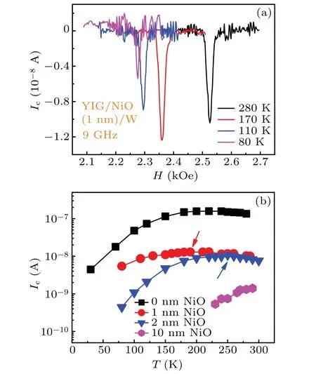
Fig. 3. (a) At f =9 GHz, the magnetic field dependence of the Ic for the YIG/NiO(1 nm)/W sample with different temperatures,(b)the temperature dependences of the Ic for the YIG/NiO(tNiO)/W samples with tNiO from 0 to 10 nm. The peak value TM of YIG/NiO(tNiO)/W samples with tNiO=1 nm and 2 nm indicated by arrows.
We further study the temperature effect on spin transport of those four YIG/NiO (tNiO)/W (tNiO=0 nm, 1 nm, 2 nm,and 10 nm)samples. As we all know,due to finite size effects,the intrinsic N´eel temperatureTN(tNiO) of the isolated thin NiO layer is reduced with decreasing NiO thickness.[22,23]The previous reports found theTNof 1–2 nm NiO film(TN(1 nm)≈170 K,TN(2 nm)≈260 K andTN(10 nm)>300 K).[9,24,25]And, 280 K (near the room temperature) mentioned above is higher than theTNof 1–2 nm NiO film. It is expected that spin pumping may be strongly affected aroundTNof the AF NiO for YIG/NiO/W system. Therefore,in the following,we perform FMR spin pumping measurements over a wide temperature range from 30 K to 300 K to explore temperaturedependent spin pumping signalsIc. Figure 3(a) shows the representative results ofHvs.Icspectra for the YIG/NiO(1 nm)/W sample with various temperatures of 80 K, 110 K,170 K,and 280 K,respectively. Instead of a monotonic trend,theIcseemingly exhibits a broad maximum at around 170 K[Fig.3(b)].Besides,Hrdecreases with decreasing temperature due to the increase of the YIG magnetization and the exchange coupling effect between YIG and NiO with decreasing temperature.
Temperature dependences ofIcat the FMR point for all four YIG/NiO(tNiO)/W(tNiO=0 nm,1 nm,2 nm,and 10 nm)samples are extracted and summarized in Fig.3(b). As shown in Fig. 3(b), all YIG/NiO/W samples are strong temperaturedependent and sensitive to the NiO layer thickness. Temperature dependence of ISHE signalIcof YIG/NiO/W trilayers exhibits a maximum at a temperatureTM. TheTMis comparable to the reducedTN(tNiO)of NiO free film. The observedTMfortNiO=1 nm and 2 nm samples are at 190 K and 250 K,respectively. And theTMincreases monotonically with the NiO thickness, consistent with the previously reported magnetic properties of NiO thin films.We note that the studied 10-nm NiO sample exhibits monotonical increases up to our highest accessible temperature of 300 K,suggesting a peak above RT. This is consistent with the 10-nm thick NiO film with a highTNabove RT. These similar temperature-dependent behaviors with an enhancement ofIcnearTNhave been observed in YIG/NiO/Pt.[9]And Our FMR spin pumping experiments are carried out with the radio-frequency. So,these phenomena demonstrate that in antiferromagnetic insulators,the spins are transported dominantly by incoherent thermal magnons rather than coherent THz AFM dynamics.[7,9,26–28]In addition, our experimental results in Fig.3(b)show thatIcis strongly suppressed towards lower temperatures. From Figs.2(a)and 3(b),although 1–2 nm NiO is a paramagnetic insulator at high temperatures aboveTN,there are still obvious ISHE signalIc. The reason is that thermal magnons continuously evolve into thermal spin fluctuations, which would transportJsat high temperatures aboveTN.[7,9]We want to emphasize that, in the whole range of experimental temperatures, inserting the thin NiO layer(even 1-nm thick)always suppresses the spin transport from YIG to W layer in YIG/NiO/W trilayer systems,as the same with the above discussed for the results obtained at RT (280 K). It is unlike the YIG/NiO (1–2 nm)/Pt system reported previously, where the enhancement of injected spin current occurs. As for YIG/W bilayer, the overall decreasing trend ofIcis primarily ascribed to the increase of the magnetic dampingαYIG/Wwith decreasing temperature. And the spin relaxation attributed to rare-earth ions induces a reduction in spin pumping efficiency. The previously reported the moderate dependence ofMsof YIG, spin Hall angleθSHand the spin diffusion lengthλSDof W on temperature are not dominant factors for the decreasing behavior ofIcwith temperature decreasing.[29–32]
The spin pumping experiments can further get the linewidth ∆Hof the magnetization dynamics for the studied multilayers. Figure 4 displays the experimental ∆Has a function of temperature for the YIG/NiO (tNiO)/W samples withtNiO=0 nm, 1 nm and 10 nm atf=9 GHz. We found that the ∆Hof the YIG/W has a slight decrease from 280 K down to approximately 120 K,and then dramatically increases with decreasing temperature. In general, the linewidth ∆H(full width at half maximum) can be described by the following equation:[30,34]

where ∆Hinhis the inhomogeneous broadening,and independent of the resonance frequencyf. The temperature dependence of the linewidth ∆Hcan indirectly reflect temperaturedependent magnetic dampingα. In general, the ∆Hinharises from magnetic inhomogeneities owing to local variations of the magnetization and anisotropy constants, and their strong temperature dependences will lead to the increase of ∆Hinh,particularly at low temperature.[32,35,36]In addition,the strong temperature-dependent damping from rare-earth ion of YIG causes a significant increase of the linewidth ∆Hin previous reports.[32,33]The enhancement of ∆Hdue to inhomogeneity is supposed to be small compared with that of rareearth ions. As for the YIG/NiO (tNiO)/W (tNiO=1 nm, and 10 nm) samples, our results in Fig. 4 show that the ∆Hstays almost invariant from about room temperature to the temperature(125 K for 1 nm and 225 K for 10 nm)at which the signalIcdisappears,indicating that the YIG/NiO exchange coupling induced-extra damping is small during temperature range of 300–125 K.[18,19]

Fig.4. Temperature dependences of the ∆H for the YIG/NiO(tNiO)/W samples with tNiO=0 nm(red and pink circles),1 nm(blue triangle),and 10 nm(green diamond)at f =9 GHz.
In summary, we have investigated the variation of ISHE signalIcYIG (0.9 µm)/NiO (tNiO)/W (6 nm) (tNiO=0 nm,1 nm, 2 nm, 10 nm) in a broad temperature range 300–30 K by utilizing the FMR spin pumping method. The value ofIcfor YIG/NiO/W samples exhibits a broad maximum at the temperatureTMnear the N´eel temperature of NiO, suggesting that spin magnons of the insulating AF NiO dominate its spin transport. TheIcexhibits a obvious decrease over the entire experimental temperature range when the NiO layer is inserted between YIG and W.And the significant suppression of the spin current transmission in the YIG/NiO(tNiO=1 nm,2 nm)/W system is in sharp contrast to the enhancement in YIG/NiO (tNiO≈1–2 nm)/Pt and Ta systems, suggesting the interfacial effects of NiO/W (e.g., interfacial spin scattering,spin memory loss,and spin conductance)dominate spin transport rather than the bulk NiO layer with a low spin loss. Our results reveal that the amplification or inhibition of spin transport in various magnetic heterostructures closely depends on the specific interface-related materials.
Acknowledgements
We acknowledge support from the National Natural Science Foundation of China (Grant Nos. 11774160, 61427812,61805116, 12004171, 61774081, and 62171096), the Natural Science Foundation of Jiangsu Province of China(Grant No. BK20192006), the National Key Scientific Instrument and Equipment Development Project of China(Grant No. 51827802), the Natural Science Foundation of Jiangsu Province of China (Grant Nos. BK20180056 and BK20200307), the Applied Basic Research Programs of the Science and Technology Commission Foundation of Jiangsu Province,China(Grant No.BK20200309),the Open Research Fund of Jiangsu Provincial Key Laboratory for Nanotechnology, the Scientific Foundation of Nanjing University of Posts and Telecommunications(NUPTSF)(Grant No.NY220164),and the State Key R&D Project of Guangdong, China(Grant No.2020B010174002).
杂志排行
Chinese Physics B的其它文章
- Editorial:Celebrating the 30 Wonderful Year Journey of Chinese Physics B
- Attosecond spectroscopy for filming the ultrafast movies of atoms,molecules and solids
- Advances of phononics in 20122022
- A sport and a pastime: Model design and computation in quantum many-body systems
- Molecular beam epitaxy growth of quantum devices
- Single-molecular methodologies for the physical biology of protein machines