Asymmetrical photonic spin Hall effect based on dielectric metasurfaces
2022-12-28GuangzhouGeng耿广州RuhaoPan潘如豪WeiZhu朱维andJunjieLi李俊杰
Guangzhou Geng(耿广州) Ruhao Pan(潘如豪) Wei Zhu(朱维) and Junjie Li(李俊杰)
1Beijing National Laboratory for Condensed Matter Physics,Institute of Physics,Chinese Academy of Sciences,Beijing 100190,China
2School of Electronic and Electrical Engineering,Wuhan Textile University,Wuhan 430200,China
Keywords: dielectric metasurface,photonic spin Hall effect,asymmetrical optical response
1. Introduction
The photonic spin Hall effect (PSHE), associated with photonic spin–orbit interactions, has attracted extensive research interest due to its potential for novel photonic applications. Generally, the spin–orbit interaction is typically related to two types of geometric phases: the propagation phase and the Pancharatnam–Berry (PB) phase, which are associated with the propagation direction and polarization state of light, respectively.[1–4]The PSHE is rising as a promising platform for novel photonic functions and can be applied in numerous applications,[5–8]such as identifying the graphene layer numbers,[9]precise measurement of optical conductivity of atomically thin crystal,[10]detection of chemical reaction rate,[11]and measurement of ion concentration.[12]More recently, the PSHE has also been applied in high-contrast edge imaging.[13]However, it is always a challenge to manipulate the PSHE flexibly in practical applications. Conventional PSHE manipulation methods only support symmetric photon spin–orbit interactions, which makes it difficult to use different spin states for multifunctional integration. By independently manipulating the different spins of light by employing the PB phase and propagation phase simultaneously,asymmetrical PSHE can integrate circular asymmetric transmission and wavefront shaping,showing strong abilities in the multidimensional and flexible manipulation of spin photons and has potential applications in chiral spin-controlled microscopy and nanophotonics.[14,15]
Recently, metamaterials consisting of subwavelength units with tunable electromagnetic responses have shown great and flexible abilities to modulate the amplitude, phase and polarization of electromagnetic waves due to the abundant local resonances, resulting in the realization of many extraordinary properties, which are unavailable through natural materials.[16–19]Compared with metamaterials composed of complex three-dimensional structures, metasurfaces are twodimensional artificial planar nanodevices, which can be easily fabricated through conventional semiconductor fabricating processes. Their optical properties are determined by an ultra-thin layer of building blocks with delicately designed geometry and arrangement,[20–22]showing advantages in controlling light in nanoscale. Metasurfaces have also exhibited excellent ability to manipulate the spin–orbit interaction of light, and have been widely used to produce spin-dependent splitting.[23,24]What is more, all-dielectric metasurfaces are composed of building blocks with high aspect ratio, highrefractive-index, and low-loss dielectrics, which have been proposed as a more prospective route than the metallic ones,for the Ohmic damping could be avoided.[25–29]Among dielectric materials used to manufacture metasurfaces, amorphous silicon (a-silicon) is commonly chosen for its compatibility with current fabrication processing technology,as well as the high refractive index and negligible absorption coefficient in the infrared region. Consequently, a-silicon now serves as a promising candidate for metasurface that can manipulate light with high-efficiency over nanoscale dimensions,showing plenty of potential applications in various nanophotonic devices such as lithography, dynamic information display and virtual reality.[30–33]
In this work, we design, fabricate, and experimentally demonstrate an optical all-dielectric a-silicon metasurface,which realizes PSHE with transmissive modulation, showing an asymmetric transverse spin-dependent split of transmitted left-handed circular polarization(LCP)light and right-handed circular polarization(RCP)light. Due to the combined action of both PB phase and propagation phase, when the metasurface is under normal incidence of operating light with wavelength of 1550 nm, the LCP light exhibits an anomalous refraction of 28.9◦,while the RCP light transmits directly. The metasurfaces with building units of a-silicon nanofins, which have changing rotational angles and feature sizes,standing on a quartz substrate are manufactured by common electron beam lithography (EBL), metal deposition and etching procedures,which are compatible with mature semiconductor processes and are feasible for on-chip integrated devices. The experimental results show good consistency with the simulation,exhibiting versatile potentials in ultra-compact spin-dependent photonics devices,and providing a simple and promising route for applications in optical sensing, optical communications,quantum information processing,etc.
2. Fabrications and method
Sample fabrication Firstly, 800 nm a-silicon was deposited onto the quartz substrates by plasma enhanced chemical vapor deposition (PECVD), then poly (methylmethacrylate)(PMMA)electron beam resist(EBR)of 400 nm was spinning coated on the a-silicon films. The desired metasurface was patterned by utilizing electron beam lithography (EBL)(JEOL 6300FS) at a base dose of 1000 µC/cm2with an accelerating voltage of 100 kV. After the exposure process, the resist was developed in methyl isobutyl ketone (MIBK): isopropyl alcohol (IPA) of 1:3 solution for 40 s and rinsed in IPA for 30 s successively,followed by a deposition of 100 nm Cr by using the electron beam evaporation deposition (EBD)method. For the purpose of realizing the lift-off process, the samples were immersed in hot acetone of 65◦C and cleaned by ultrasonic. Finally,by etching through the inductively coupled plasma (ICP) reactive ion etching (RIE) method with HBr at room temperature(RT)for 270 s(flow rate of 50 sccm, pressure of 10 mTorr, RF and ICP powers of 50 W and 750 W,respectively), the desired metasurfaces were transferred from Cr to silicon and the residual Cr was removed by cerium(IV)ammonium nitrate.
Simulation methods The phase responses and crosspolarized transmission efficiency of the metasurface were simulated by the three-dimensional (3D) finite difference timedomain method (FDTD). A two-dimensional (2D) parameter sweep of a single unit with length and width from 80 nm to 250 nm and 200 nm–650 nm,height fixed at 800 nm simultaneously,was carried out under thex-polarization to obtain the phase map of the different structural parameters at 1550 nm wavelength under normal incidence. For these simulations,periodic boundary conditions were applied in thexandydirections and perfectly matched layers(PMLs)were applied in thezdirection. The phase response undery-polarization was obtained by transposition of thex-polarization results. The refractive index of the a-silicon was measured by an ellipsometer. The effective refractive index was obtained from the fundamental modes while the power coupling into higher-order waveguide modes was ignored.
3. Results and discussion
Figure 1 shows the designed transmissive all-dielectric metasurface that achieves asymmetrical transverse spindependent split due to the spin–orbit interaction in a broadband waveband. In this work, four diverse unit building blocks labeled as U1–U4 are specifically selected to assemble the metasurface, which stand on the quartz substrate. The periodsPand heightsHare both kept at 800 nm, while the widthsWand lengthsLof U1 to U4 are set as 220 nm/290 nm/320 nm/340 nm, and 600 nm/530 nm/540 nm/550 nm,respectively. One supercell,which possesses four nanofins with aπ/8 increment gradient of the rotation angleθaround thez-axis, is arrayed in large area to achieve the designed metasurface. To obtain appropriate PB phase, the rotation anglesθare kept at 0,π/8,π/4,and 3π/8,successively.
When LCP or RCP lights illuminate the metasurface,the two spins of light will be refracted into the different transverse propagating directions after passing through the metasurface.For normal incident circular polarization(CP)light,the transmitted electric field(EtL/R)of the nanofins rotated by an angleθcan be obtained from the Jones matrix as follows:[34,35]


Additionally, when an optical wave with CPs incident on a certain nanofin, the relationship between the modulated phase and the characteristics of the nanofin can be achieved as follows:[36]
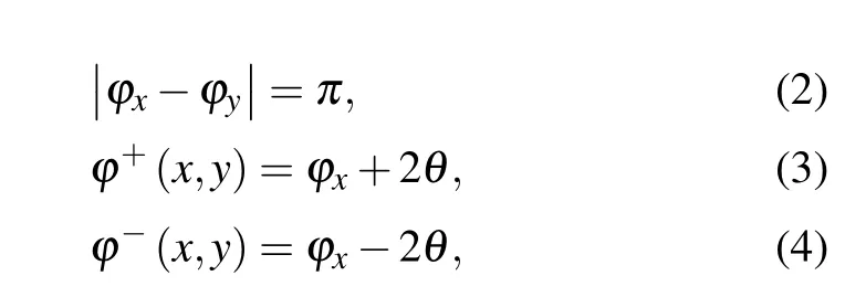
whereϕxandϕyrepresent the phase delays of the nanofin for polarized light along thexandyaxes, respectively.θis the rotation angle of the nanofin relative to the reference coordinate system, andϕ+(x,y) andϕ−(x,y) are the corresponding transmitted modulated phases. It can be seen from the above equations that the phase difference betweenϕxandϕyisπ. The modulation phase depends onϕxand 2θ, which corresponds to the propagation phase and the PB phase, respectively. The propagation phaseϕxis mainly determined by the material refractive index and the geometry of the nanofin,and the PB phase 2θis only determined by the rotation angle of the nanofin. Resultingly, the LCP and RCP lights are transformed into the corresponding orthogonal polarization states after passing through the nanofin,while gaining the same propagation phase and opposite PB phase. According to the above equations,the independent phase modulation of the LCP and RCP light can be obtained through the linear combination of the propagation and PB phases.

Fig. 2. The design and simulation mechanisms of nanofins. The simulation results of (a) transmission Tx/Ty (b) phase delays ϕx and ϕy as a function of lengths Lx/Ly of nanofins under normal incidence at the wavelength of 1550 nm,respectively. The sizes of the selected nanofins are highlighted by red dots.(c)Simulated E-fields(top: xoz-plane,bottom: yoz-plane)distributions in and near the nanofin at the wavelength of 1550 nm.
According to the above discussion, a series of nanofins with different phases (ϕx,ϕy) that satisfy Eqs. (2)–(4) possessing complete phase coverage ofϕ+(x,y) andϕ−(x,y)are required. To achieve the maximum polarization conversion efficiency (PCE), every nanofin is supposed to operate as a half-waveplate. The 3D finite difference time-domain(FDTD) is implemented to investigate the geometric parameters of the nanofins. The transmissionsTx/Tyand the phase changesϕxandϕyare simulated as a function of the lengthsLx/Lyof the nanofins,respectively. The proper parameters of the nanofins are picked up through these lengths,as illustrated by red dots in Figs. 2(a) and 2(b). The nanofins U1–U4 possess relative propagation phase shiftsϕxof 0,π/4,π/2 and 3π/4 in thex-direction, respectively. While the phase delayϕyin they-direction meets Eq. (2) to get high polarization conversion efficiency. Furthermore, localized electric fields distributions atxozplane(top in Fig.2(c))andyozplane(bottom in Fig.2(c))in the nanofin at the wavelength of 1550 nm illustrate well confinement of electric fields,showing that the coupling between adjacent nanofins is weak. In this way, the non-uniform medium is typically approximated to the uniform periodic medium,which simplifies the design process.

Fig. 3. The as-fabricated a-silicon metasurfaces composed of different nanofins, and the simulated/experimental PCEs of each nanofin array. (a)Tilted scanning electron microscopy(SEM)images of different metasurfaces composed of nanofins U1–U4,respectively. The insets are the top view SEM images of each metasurfaces. (b) Simulated and experimental PCEs of the metasurfaces composed of nanofins of U1–U4. Scale bars: 1µm.
To further establish the validity of the selected U1–U4 nanofins, the a-silicon nanofins are separately fabricated on quartz substrates, as shown in Fig. 3(a). The optical measurements of PCEs are carried out by the Fourier transfer infrared spectrometer (FTIR). The PCEs of U1–U4 are firstly calculated for incident light wavelengths from 1300 nm to 2000 nm, showing that samples U1–U4 have maximal PCEs at the promised operating wavelength(∼1550 nm),as shown in the top of Fig.3(b).The PCE is calculated as the ratio of the transmitted opposite helicity power to the incident power. The measured PCE results are displayed at the bottom of Fig.3(b).The deterioration of intensity between simulation and measurement is mainly caused by imperfection of fabrication such as the structure distortions, while the trends match well with the maximum PCE at the operation wavelength.
Usually,two types of transverse spin-dependent splittings based on the metasurface (symmetric and asymmetric) are concerned. As for the symmetric spin-dependent splitting,the nanofins in the supercell are reserved of the uniform geometric structures with different orientation angles. The light with different helicity obtains an opposite but equal refraction angle after transmitting through the metasurface.[30]However,the refraction angles of light with different spin states are different along theyozplane in the asymmetric case, in which the refraction angles are more flexible. Due to the variation of nanofins in the supercell, the modulated phase is a hybrid phase(the PB phase and propagation phase)for the asymmetric case.[32]
These four designed nanofins show relatively high PCE,and also introduce different extra propagation phases. The combination of PB phase and propagation phase makes it much more flexible to modulate the polarization of light,implying multi-freedom regulation in spin photons, such as PSHE.To further verify that the propagation phase can break the conjugated characteristic of the modulated phases,the chosen nanofins,whose propagation phase shifts are 0,π/4,π/2,and 3π/4 in thex-direction, respectively, are arranged with aπ/8 increment of the rotation angle to fabricate the metasurfaces as shown in Fig.4(a). Combined with the PB phase,the transmitted modulated phase of LCP light can cover 2πphase,while the transmitted phase of RCP light will remain the same,through which the transmitted LCP light exhibits an anomalous refraction while the RCP light transmits directly. We simulate the electric field distributions of the transmitted lights for the LCP and RCP incident lights,in which the conjugated characteristic of modulated phases of PB phase metasurfaces for different spins is broken,and transverse asymmetrical spindependent splitting occurs,as illustrated in Fig.4(b). The refractive angles of the transmitted LCP light can be calculated by the generalized Snell’s law asθ′=sin−1(λ/Λ)=28.9◦,whereΛis the periodic dimension of each supercell, which equals to 4 times of the periodP. Figure 4(c) shows the experimental intensity distributions for normal RCP and LCP illuminations, respectively. These two spins of light are split into the transverse asymmetric propagating directions after passing through the metasurfaces. What is more, by properly optimizing the geometric dimensions of the nanofins,the reflective angles of the LCP and RCP lights can be modulated independently. The above results show highly free manipulation of spin photons and realize multidimensional spindependent splitting. It provides a flexible way to design spindependent multifunctional devices for a variety of potential applications, including optical sensing, microscopy imaging,and spin-controlled nanophotonics.

Fig. 4. Fabricated a-silicon metasurface and transmitted light results with different spin states illumination at 1550 nm. (a) Tilt SEM images of the metasurface for abnormal refraction, and the insets are the corresponding top-down SEM images. (b)Simulated electric field maps for RCP and LCP illuminations,respectively. (c)Measured light intensity profiles of m=−1,m=0,and m=+1 orders with incident polarization states of RCP and LCP,respectively. Scale bar: 1µm.
4. Conclusion
We have demonstrated a multi-dimensional polarization manipulation device based on a single-layer dielectric metasurface.The incident circularly polarized light of two different polarizations can be arbitrarily and independently modulated due to the combination of the PB phase and the propagation phase. Compared with the previous works which control the polarization of the light only by the PB phase,the metasurface we proposed enables to control the polarization more flexible due to the collaborative work mode of the PB phase and propagation phase. The conjugated characteristic of the modulated PB phase for different spin photons can be successfully broken due to the interplay of the propagation phase and the PB phase, by which the spin-dependent splitting in the transverse direction can be completely controlled. Our approach has potentials in spin-controlled nanophotonics,ranging from microscopy imaging to optical communication and information encryption.
Acknowledgments
Project supported by the National Natural Science Foundation of China (Grant Nos. 12074420, U21A20140, and 61905274), the Beijing Municipal Science & Technology Commission, Administrative Commission of Zhongguancun Science Park (Grant No. Z211100004821009), the Chinese Academy of Sciences through the Project for Young Scientists in Basic Research (Grant No. YSBR-021), and the Synergic Extreme Condition User Facility.
猜你喜欢
杂志排行

Chinese Physics B的其它文章
- Editorial:Celebrating the 30 Wonderful Year Journey of Chinese Physics B
- Attosecond spectroscopy for filming the ultrafast movies of atoms,molecules and solids
- Advances of phononics in 20122022
- A sport and a pastime: Model design and computation in quantum many-body systems
- Molecular beam epitaxy growth of quantum devices
- Single-molecular methodologies for the physical biology of protein machines