Impact of incident direction on neutron-induced single-bit and multiple-cell upsets in 14 nm FinFET and 65 nm planar SRAMs
2022-12-28ShaoHuaYang杨少华ZhanGangZhang张战刚ZhiFengLei雷志锋YunHuang黄云KaiXi习凯SongLinWang王松林TianJiaoLiang梁天骄TengTong童腾XiaoHuiLi李晓辉ChaoPeng彭超FuGenWu吴福根andBinLi李斌
Shao-Hua Yang(杨少华) Zhan-Gang Zhang(张战刚) Zhi-Feng Lei(雷志锋) Yun Huang(黄云)Kai Xi(习凯) Song-Lin Wang(王松林) Tian-Jiao Liang(梁天骄) Teng Tong(童腾)Xiao-Hui Li(李晓辉) Chao Peng(彭超) Fu-Gen Wu(吴福根) and Bin Li(李斌)
1School of Physics and Optoeletronic Engineering,Guangdong University of Technology,Guangzhou 510006,China
2Science and Technology on Reliability Physics and Application of Electronic Component Laboratory,China Electronic Product Reliability and Environmental Testing Research Institute,Guangzhou 510370,China
3Institute of Microelectronics of Chinese Academy of Sciences,Beijing 100029,China
4Institute of High Energy Physics,Chinese Academy of Sciences,Beijing 100049,China
5Spallation Neutron Source Science Center,Dongguan 523803,China
6School of Microelectronics,South China University of Technology,Guangzhou 510640,China
Keywords: neutron,fin field-effect transistor(FinFET),single event upset(SEU),Monte–Carlo simulation
1. Introduction
Atmospheric neutron-induced single event effects (SEE)in avionics and key ground electronics are gaining increasing attention, due to the fact that the SEE performance of an integrated circuit (IC) becomes worse as the feature size shrinks.[1,2]Hence, the evaluation of real-time neutroninduced SEE sensitivity in the applied environments, especially for nanometric ICs,can be very important for the system reliability insurance.
To measure the atmospheric radiation induced soft error rate(SER),accelerated testing can be conveniently performed by using the ground-based neutron sources.[3]While clear differences exist between neutrons from ground-based neutron sources and real atmosphere,such as incident direction,energy spectrum,etc.It can be predicted that single event upset(SEU)response is affected by the incident direction of neutron,since that upsets are produced by secondary particles generated by nuclear reactions between neutrons and their traversing materials. Consequently, understanding the impact of incident directions on SEE is critical in several aspects: (1)guiding the ground-based testing, and (2) selecting the “best incident direction”,which can be conveniently utilized to reduce the SER by the selection of board orientation during equipment setup.
In the past, angular dependence of neutron-induced SEE was reported by several research groups.[4–8]In 2019, S.Abe[9]reported that the number of SEUs in 65 nm static random-access memory (SRAM) obtained by the board-side irradiation was approximately 20% to 30% smaller than that obtained by irradiation on the plastic package side, by using quasi-monoenergetic neutrons. Tibetan-Plateau based realtime testing[10]and accelerated testing of 65 nm quad data rate(QDR)SRAMs[11]were conducted to reveal the SEU characteristics and mechanisms in our previous publications. The 14 nm fin filed-effect transistor (FinFET) SRAMs were also irradiated by neutrons at normal incidence.[11]However, few publications focused on the impact of incident direction on neutron-induced SEE response in advanced FinFET technology.
In this work,the impact of incident direction on neutroninduced single-bit upsets (SBU) and multiple-cell upsets(MCU)in 14 nm FinFET SRAM and 65 nm QDRII+SRAM is studied in a comparative way, by experiments at the BL09 terminal of China Spallation Neutron Source (CSNS) and Monte–Carlo simulations.
2. Experimental setup
2.1. Devices under test
Parameters of the tested SRAM devices are showed in Table 1. Note that,the 14 nm FinFET SRAM is packaged inflip-chip ball grid array (BGA), with the substrate thinned to 60µm(designed for previous heavy-ion testing). The 65 nm SRAM is packaged in wire-bonded BGA,and the plastic package above the chip was not etched before irradiation.

Table 1. Parameters of the tested SRAM devices.
2.2. Experimental setup
The experiment was conducted at the BL09 terminal of CSNS.The simulated neutron energy spectrum of BL09 at irradiation position is shown in Fig.1,which is obtained by simulation based on the actual setup. The beam flux during the experiments is fixed, with a total of 2.8×10⁷n/(cm2·s). The flux of thermal neutrons (E<0.4 eV) is 2.7×10⁶n/(cm2·s),and the flux of high energy neutrons (E> 10 MeV) is 1.1×10⁵n/(cm2·s). During the irradiation, the thermal neutrons can be selected to be filtered,by inserting cadmium(Cd)film (∼2 mm) into the beam. After passing through the Cd film,neutrons with energy below 0.4 eV are eliminated.While the energy spectrum in theE>10 MeV region is basically unchanged since Cd film has a cutoff energy of 0.4 eV.[3]Specifically,for the 14 nm FinFET SRAM,the thermal neutrons were not filtered during irradiation, since that the irradiated device under test(DUT)was sensitive to thermal neutrons. While for the 65 nm QDRII+SRAM,the thermal neutrons were filtered,since that the irradiated DUT was immune to thermal neutrons,as reported in our previous publication.[11]

Fig. 1. The simulated neutron energy spectrum at irradiation position of the BL09 terminal of CSNS.
Figure 2 illustrates three kinds of incident directions during neutron irradiation: front, back and side. Additionally,Table 2 lists the layers that neutrons penetrate before reaching the sensitive volume(SV),for different incident directions.Note that, due to the different package of the two DUTs (see Table 1), the layers that neutrons penetrate before reaching the SV can be quite different, even under the same incident direction. For the 14 nm FinFET SRAM, the BGA package includes solder ball (with a diameter of∼0.8 mm), substrate (∼0.7 mm), and small solder ball (with a diameter of∼0.08 mm), along the direction of neutron incidence. The detailed metallization struture of the 14 nm FinFET SRAM is shown in Fig. 10(a). Eight layers of metal wiring can be seen,and the majority of the metal materials are copper.Tungsten plugs are found between M0 and the active silicon layer.The total depth of the mentalizations is about 6.3µm. For the 65 nm QDRII+SRAM,the BGA package includes solder ball(with a diameter of∼0.9 mm)and substrate(∼0.5 mm),following the direction of neutron incidence. Six layers of metallization are found,and the majority of the metal materials are copper. Tungsten plugs are found between M0 and the active silicon layer. The total depth of the mentalizations is about 7.1 µm. As examples, Figs. 3 and 4 show the pictures of the 14 nm FinFET SRAM and the 65 nm QDRII+SRAM under side direction irradiation,respectively.
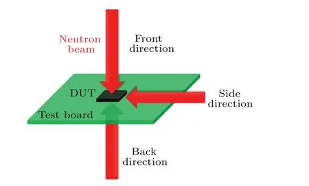
Fig.2. Three kinds of incident directions during neutron irradiation.

Table 2. Layers that neutrons penetrate before reaching the SV,for different incident directions.

Fig.3. The 14 nm FinFET SRAM under irradiation(side direction).
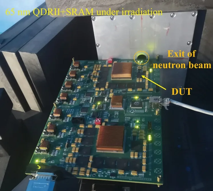
Fig. 4. The 65 nm QDRII+SRAM under irradiation (side direction).Note that,the test board was designed also for high-altitude experiment and only the arrowed DUT of the 18 loaded devices was tested.
Checkerboard pattern was written into the DUT before irradiation, and contents of the DUT were read and compared with the golden data periodically during the neutron bombardment. The detailed SEU information including the error time,address and data were reported. In addition, the device currents were monitored continuously and no single event latchup(SEL)was observed during all the tests. The ambient temperature was controlled at 25±5◦C.
3. Experimental results and analysis
3.1. SEU cross sections
Figure 5 shows the neutron-induced SEU cross sections in the 14 nm FinFET SRAM under different incident directions.Obviously,back incidence is the“worst case”,with SEU cross section 1.7–4.7 times higher than those of front and side incidences.The reason that side incidence exhibits the lowest SEU cross section is discussed here. In the 14 nm FinFET SRAM,neutron-induced electron–hole pairs are collected by both drift and diffusion processes. For side incidence,the generated secondary particles by high energy neutron tend to traverse the fin from the side. Hence,for most cases,the generated electron–hole pairs are collected by drift or diffusion process, depending on the location of the ion trajectory (in the fin or in the substrate). However,for front and back incidences,the trajectory of secondary particle tends to cross both the fin and the substrate. Electron–hole pairs can be collected by both drift and diffusion processes, resulting into higher SEU cross sections.
Note that,the SEU cross section is calculated by counting the MCU as separate soft errors and using the total neutron flux of 2.8×10⁷n/(cm2·s). It should be noted that the SEU cross sections include the contribution of thermal neutrons.

Fig. 5. Neutron-induced SEU cross sections in the 14 nm FinFET SRAM under different incident directions.

Fig. 6. Neutron-induced SEU cross sections in the 65 nm QDRII+SRAM under different incident directions.
Figure 6 shows the neutron-induced SEU cross sections in the 65 nm QDRII+SRAM under different incident directions. Differently, front incidence is the “worst case”, with SEU cross section 1.7–1.8 times higher than those of back and side incidences. Note that, the SEU cross sections are calculated by using the high energy neutron(E>10 MeV) flux of 1.05×10⁵n/(cm2·s). The reasons are that: (1) the 65 nm QDRII+SRAM is immune to thermal neutron, as reported in our previous publication,[11]and (2) high energy neutrons(E>10 MeV)are the main contribution of soft error rate, as specified in the JESD89A standard.[3]
Comparing Figs.5 and 6,it seems that the worst incident direction for the 14 nm FinFET technology and the 65 nm planar technology is opposite. However, combining the above results with Table 2,it can be found that the worst incident direction corresponds to the case that neutrons traverse package and metallization before reaching the SV. In order to further reveal the underlying mechanisms, Monte–Carlo simulations are conducted,which are shown in Section 4.
3.2. MCU characteristics
MCU ratios of 14 nm FinFET SRAM and 65 nm QDRII+SRAM under different incident directions are shown in Figs.7 and 8, respectively. Obviously, most of the MCU events are double-bit upsets (i.e., MCU2). The largest MCU for the 14 nm FinFET SRAM involves 8 bits,while the largest MCU for the 65 nm QDRII+SRAM involves 4 bits. For MCU response,side incidence is the“worst case”. Here,“worst case”corresponds to the case with highest MCU ratio,because more MCU events mean more bit-flips, and more error correcting code(ECC)resource must be used to eliminate them.The phenomenon can be explained by that neutrons at side incidence are most likely to traverse and affect multiple SVs, since that majority of the secondary particles generated by the interactions between spallation neutrons and DUT are moving forward. Since that large MCU event is relatively rare,the probability of MCU≥4 under back incidence in Fig.7 is higher than that under side incidence,due to the poor statistics.
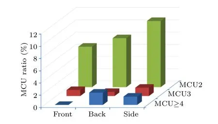
Fig. 7. MCU ratios of the 14 nm FinFET SRAM under different incident directions.

Fig.8. MCU ratios of the 65 nm QDRII+SRAM under different incident directions.
4. Monte–Carlo simulations
Aims of Monte–Carlo simulations of the neutron transport are investigating the characteristics of secondary ions in the device SV, including ion species, LET, range and making comparisons between different incident directions. This part mainly focuses on the research of 14 nm FinFET SRAM,since that Abe’s paper[9]can be referred to for the inner mechanisms of results of the 65 nm SRAM in the previous section.The main conclusions of Abe’s paper are that the atomic composition of the material placed in front of the memory chip has a considerable influence on the SER because production yields and angular distributions of secondary hydrogen (H)and helium(He)ions(the main causes of SEUs)depend on the composition. In particular, the existence of hydrides, such as plastic,considerably increases the SER because of the higher production yields of secondary H ions that are generated via elastic scattering of neutrons with hydrogen atoms.
4.1. The 3D simulation model of DUT
Simulation model of the 14 nm FinFET SRAM is built based on the reverse-technique result of DUT (see Fig. 9)and experimental setup. Reverse-technique processes include cross-section analysis and layer-grinding analysis. Crosssection analysis is used to obtain Fig. 9(a), by cutting the DUT and observing by scanning electron microscopy(SEM).Layer-grinding analysis is used to obtained Fig.9(b),by grinding the DUT to polysilicon layer and observing by SEM. In Fig.9(a),eight layers of metallization can be seen,and the majority of the metal materials are copper. Tungsten (W) plugs are found between M0 and the active silicon layer. On the top of the Fin,high-Kmetal gate(HKMG)exists. Material of the high-Kgate oxide is HfO2with a depth of 1.9 nm. Material of the metal gate is TiN with a depth of 4.6 nm. The total depth of the mentalizations is about 6.3µm.
Table 3 shows the memory cell sizes and SV parameters of the 14 nm FinFET SRAM. The drain of the off-state Nchannel metal oxide semiconductor(NMOS)transistor is considered to be the SV of one memory cell. The depth of the SV is set as the fin height. Importantly,note that the LET threshold of the DUT is smaller than 0.5 MeV·cm2/mg, making it sensitive to proton direct-ionization effect.
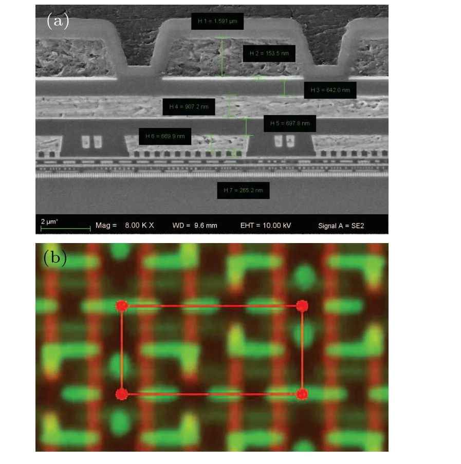
Fig.9. (a)Cross section and(b)polysilicon layer images of the 14 nm FinFET SRAM.

Table 3. Memory cell sizes and SV parameters for the 14 nm FinFET SRAM.
4.2. Neutron transport simulations
Neutron transport process is simulated by the Geant4 toolkit.[12]Thex×yscale of the device model is set as scales of the SV,in order to improve the simulation efficiency. A total number of 109neutrons strike the surface of device model normally. Typical neutron energies are selected in the simulation, including 5 MeV, 100 MeV, 500 MeV, and 1 GeV.The reasons are that for the 14 nm FinFET SRAM,upsets are mainly induced by thermal neutrons and high energy neutrons.Considering the low critical charge of the device,5 MeV neutrons are also simulated. Thermal neutrons are not simulated because that thermal neutrons induce upsets by the products of the10B(n,α)7Li reaction. In this reaction,the alpha particle and the lithium(Li)nucleus are emitted in roughly opposite directions to conserve momentum.[13]The outgoing directions of the products exhibit random distribution. Thus,under different incident directions of thermal neutrons, characteristics of the reaction products in the device SV are basically the same.
The characteristics of secondary ions in the device SV,including ion species, LET, and range under different incident directions are obtained. Note that, side incidence is not simulated in this paper and will be investigated in the future,because that under side incidence, neutrons traverse different depths of silicon before reaching the SVs of the DUT, which means that the situations for all the SVs are not same. Nevertheless,as can be seen in Table 2,front incidence is similar to side incidence for the 14 nm FinFET SRAM,and the simulation results can be referred to.
5. Simulation results
Figures 1 and 11 compare the secondary ion species in SV of the 14 nm FinFET SRAM induced by incident neutrons with various energies,for front incidence and back incidence,respectively. The impact of incident direction is obviously shown. The total yield of secondary ions for back incidence is clearly higher than that for front incidence, by about 6×.Note the log-scale ofY-axis in Figs.1 and 11,majority of the reaction products are n,p,α,Si,Al,etc.The p andαare capable of inducing soft errors in the 14 nm FinFET SRAM,with a critical charge of 0.05 fC (see Table 3). This explains the phenomenon in Fig.5 that neutron-induced SEU cross section in the 14 nm FinFET SRAM under back incidence is higher,since that neutrons at back incidence are capable of creating more“useful”secondary ions in the device SV,and thus more upsets are induced.

Fig.10. Secondary ion species in the SV induced by incident neutrons with various energies(front incidence).

Fig.11. Secondary ion species in the SV induced by incident neutrons with various energies(back incidence).
It can also be observed that neutrons with higher energy are capable of creating more diverse secondary ion species,for both front and back incidences. Besides, for the front incidence, the heaviest secondary ion is Si. While for the back incidence, the heaviest secondary ion is W. Compared to the neutrons at front incidence, neutrons at back incidence create more various secondary ions in the SV,ranging from p to W.The inner reasons can be found in Table 2,which lists the layers that neutrons penetrate before reaching the SV of the 14 nm FinFET SRAM, for different incident directions. For the front incidence, the material that neutrons traverse before reaching the SV is Si substrate, while for the back incidence,the intermediates are more complicated and contain various materials with high-Zelements,such as W plugs and Hf in the high-Kgate oxide. It can be confirmed that secondary ions heavier than Si are induced by nuclear reactions between incident neutrons and the metallization&HKMG on the top of the fins. This explains the phenomenon in Fig. 7 that MCU ratio of the 14 nm FinFET SRAM under back incidence is higher than that under front incidence,since(1)the total yield of secondary ions for back incidence is clearly higher than that for front incidence,including both light and heavy secondary ions, and (2) light secondary ions with long range and heavy secondary ions with enough range are both capable of inducing MCU events.
Figures 12 and 13 show the LET and range of secondary ions in the SV of the 14 nm FinFET SRAM induced by incident neutrons with various energies,for front incidence and back incidence,respectively. One symbol in the figure represents one secondary ion in the SV.It is obvious that neutrons with higher energy are capable of generating secondary ions with larger LET values, longer ranges, and thus more generated charges in the SV,with also higher probability.Moreover,clear differences can be seen between the front incidence and the back incidence.For the back incidence,the LET and range of secondary ions in the SV are showing wider distribution than that of the front incidence case,which is consistent with the previous experimental results.
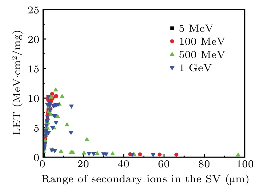
Fig.12.LET and range of secondary ions in the SV induced by incident neutrons with various energies(front incidence).

Fig.13.LET and range of secondary ions in the SV induced by incident neutrons with various energies(back incidence).
6. Implications for application
In the previous sections,we find that for both technology nodes,the“worst direction”corresponds to the case that neutrons traverse package and metallization before reaching the SV of the DUT.The SEU cross section under the worst direction is 1.7–4.7 times higher than those under other incidences.While for the MCU sensitivity,side incidence is the worst direction,with the highest MCU ratio.
This information can be conveniently utilized to reduce the SER by the selection of board orientation during equipment setup. Specially, for avionic or ground application, atmospheric neutrons are mainly flying from top to down. Thus,for most boards,placing in a reverse way(i.e.,with front side downward) seems to be a good choice since most of the ICs are not in flip-chip package. Moreover, upright setup of the board should be avoided,especially for MCU-sensitive ICs.
7. Conclusions
In this work,the impact of incident direction on neutroninduced SBUs and MCUs in 14 nm FinFET SRAM and 65 nm QDRII+SRAM is studied,by both irradiation experiment and Monte–Carlo simulation. It is found that,for both technology nodes,the“worst direction”corresponds to the case that neutrons traverse package and metallization before reaching the SV of the DUT.The SEU cross section under the worst direction is 1.7–4.7 times higher than those under other incidences.While for the MCU sensitivity,side incidence is the worst direction, with the highest MCU ratio. Further, Monte–Carlo simulations show that the presence of package and metallization results into high amount of diverse secondary ions in the device SV,and thus higher SEU and MCU cross sections. Majority of the reaction products are p,α,Si,and Al.
It seems that side incidence of neutron is the“best direction”,but the MCUs should be paid special attention to.
Acknowledgements
Project supported by the Key-Area Research and Development Program of Guangdong Province, China (Grant No.2019B010145001),the National Natural Science Foundation of China (Grant Nos. 12075065 and 12175045), and the Applied Fundamental Research Project of Guangzhou City,China(Grant No.202002030299).
猜你喜欢
杂志排行
Chinese Physics B的其它文章
- Editorial:Celebrating the 30 Wonderful Year Journey of Chinese Physics B
- Attosecond spectroscopy for filming the ultrafast movies of atoms,molecules and solids
- Advances of phononics in 20122022
- A sport and a pastime: Model design and computation in quantum many-body systems
- Molecular beam epitaxy growth of quantum devices
- Single-molecular methodologies for the physical biology of protein machines