Porous AlN films grown on C-face SiC by hydride vapor phase epitaxy
2022-08-01JiafanChen陈家凡JunHuang黄俊DidiLi李迪迪andKeXu徐科
Jiafan Chen(陈家凡), Jun Huang(黄俊), Didi Li(李迪迪), and Ke Xu(徐科)
Suzhou Institute of Nano-Tech and Nano-Bionics,Chinese Academy of Sciences,Suzhou 215123,China
Keywords: hydride vapor phase epitaxy(HVPE),porous,AlN
1. Introduction
Porous nitride semiconductor is a rapidly developing research field.[1]It has opened up a series of new properties and applications including optical reflectors,[2]sensors,[3]catalysis,[4]as well as improving the material quality.[5]AlN has potential applications in power electronic and optoelectronic fields due to its wide bandgap, high breakdown voltages, high thermal conductivity and strong resistance to radiation. Hydride vapor phase epitaxy(HVPE)is expected to be promising for fabricating AlN thick films. Several researchers have attempted to grow AlN layers through HVPE by using SiC as a starting substrate for the preparation of AlN thick films, because SiC has good thermal conductivity and chemical stability for high-temperature application conditions,and the lattice and thermal expansion mismatches between AlN and SiC are low as well.[6–8]
However, due to the tensile strain of AlN grown on SiC substrate,the growth of thick and crack free films is very challenging. Without the use of stress control techniques, cracks are likely to occur when AlN films are thicker than 3 μm.In addition, AlN grown on SiC substrate would show rough surfaces due to the low migration length of adatoms.[9]The growth temperature and V/III ratio can affect the migration length of adatoms. Porous AlN film is an effective way to relax the strain in the AlN thick films. As for the HVPE method,however, the study of porous AlN thick films is less. Here,we demonstrated porous AlN films grown on C-face SiC by HVPE. The changes of surface morphology, crystal quality and stress state of AlN films with growth condition were studied. Finally,a porous AlN film with a maximum thickness of 8 μm and without cracks was grown.
2. Experiments
AlN films were grown on 2-in diameterc-oriented C-face 6H-SiC substrates by HVPE.The growth temperature was approximately 1400°C and the growth pressure was 1 kPa. NH3and HCl were used as input active gases,a mixture of N2and H2served as carrier gas. AlCl3was formed by the reaction of Al and HCl at 550°C in the source zone of the reactor for AlN growth. The growth conditions of AlN samples were shown in Table 1.
The surface and cross-sectional morphology of the samples was characterized by scanning electron microscopy(SEM) (FEI Quanta 250 FEG) and atomic force microscopy(AFM) (Veeco Dimension 3100).The Raman spectra were measured by using a LabRAM HR 800 spectrometer(HORIBA Scientific,Edison,NJ,USA),excited with a 532 nm laser. High-resolution x-ray diffraction (HR-XRD) measurements were performed on the x-ray diffractometer(Bruker D8 Discover). The microstructure observations were performed on a transmission electron microscope(Themis Z,USA)with an accelerating voltage of 300 kV. The cross-sectional specimens for TEM measurements were prepared by mechanical polishing and followed by the Ar+ion milling process.
3. Results and discussion
Figure 1 shows the top view SEM images of AlN samples S1–S4. The surface of sample S1 grown under V/III ratio of 15 is smooth but with cracks as shown in Figs.1(a)and 1(b).As the V/III ratio increases to 30,pits appear on the surface of the AlN film, as shown in Figs. 1(c) and 1(d), corresponding to sample S2. When the V/III ratio is further increased to 60,the surface uniformity of the AlN film deteriorates and cracks appear, as shown in Figs. 1(e) and 1(f), which correspond to sample S3.Figures 1(g)and 1(h)show the SEM image of sample S4. The growth conditions of sample S4 are as the same as sample 2,excepting that the thickness is increased from 3 μm to 8 μm. After increasing the thickness,the surface morphology of the AlN film still maintains a porous morphology,and there are no cracks. It is worth noting that the suitable V/III ratio could effectively suppress the cracks of samples.
Table 1. The growth conditions of AlN films.
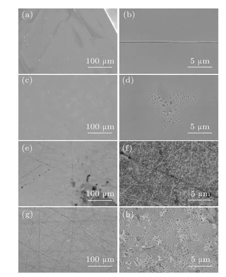
Fig.1. Plan-view SEM images:(a)and(b)sample S1,(c)and(d)sample S2,(e)and(f)sample S3,(g)and(h)sample S4.
Figure 2 shows the AFM images over areas of 10 μm×10 μm and 2 μm×2 μm for the samples S1–S4,respectively.It is observed that the sample grown under a low V/III ratio of 15 exhibited a surface with step-flow morphology as shown in Figs. 2(a) and 2(b). The samples grown at V/III ratios of 30 and 60 all show porous surface morphology, as shown in Figs.2(c)–2(f),and there are some cracks and some irregular island-like structures on the surface of the latter. Figure 1(d)shows the AFM image of sample S4. As the thickness increases, the AlN film still has a porous morphology, but the shape of the pores changes from polygonal to nearly circular. The density of the pores in sample S2, S3, and S4 is 8.45×109cm-2,3.85×109cm-2,and 1.07×1010cm-2,respectively. It is speculated that the porous morphology could originate from the difficult coalescence during growth when the V/III is high. In another word, high V/III growth would deteriorate the surface morphology and make the coalescence growth of AlN film become more difficult.[10]
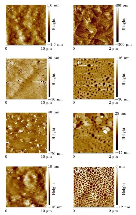
Fig.2. AFM images of AlN films: (a)and(b)sample S1,(c)and(d)sample S2,(e)and(f)sample S3,(g)and(h)sample S4.
Figure 3 shows normalized Raman spectra of the E2(high) phonon mode for all the samples. The vertical line shows the stress-free frequency of 657.4 cm-1.[6]The magnitude of each tensile stress is determined by the difference between its peak position and the stress free peak position.For biaxial stress can be estimated by
The peak positions of the E2(high) phonon mode for samples S1–S4 are 651.99 cm-1,654.97 cm-1,652.74 cm-1,and 654.25 cm-1,corresponding to the biaxial tensile stress values of 1.34 GPa,0.60 GPa,1.15 GPa,and 0.78 GPa,respectively.The peaks for all samples appear on the lower frequency side of the stress-free position,showing their residual tensile stress.Samples S2 and S4 are under the low residual stress compared with samples S1 and S3,which indicates that the formation of porous AlN could relax the stress.
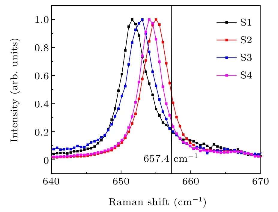
Fig.3. Normalized Raman spectra of the AlN E2 (high)phonon mode. The vertical line shows a stress-free frequency of 657.4 cm-1.
Figure 4 shows the dependence of the full width at half maximum (FWHM) of the (0002) and (10-12)-plane x-ray rocking curves(XRCs)for samples S1–S3 on the V/III ratio.Threading dislocations in AlN films are associated with local lattice distortion. Screw-component and edge-component dislocations contribute to the broadening of the (0002) and (10-12)peak,respectively. The dislocation density of AlN films is evaluated by[11]
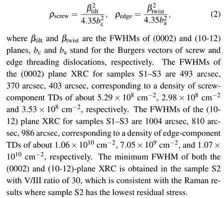
Figure 5 shows the (0002) and (1012)-plane x-ray rocking curves(XRCs)of samples S4. The FWHMs of the(0002)and (1012)-plane XRCs for sample S4 are 334 arcsec and 547 arcsec, corresponding to a density of screw-component and edge-component TDs of about 2.43×108cm-2and 2.89×109cm-2, respectively. Obviously, as the thickness increases,the crystal quality of the AlN film has been greatly improved.
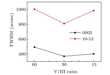
Fig. 4. The FWHM values of (0002) and (10-12) x-ray diffraction rocking curves of samples S1–S3.
Fig.5. The(0002)and(1012)-plane XRCs of sample S4.
Figure 6 shows cross-sectional SEM and TEM pictures of sample S4. It can be seen from the cross-sectional SEM and TEM that the pores on the surface of the AlN film are similar to V-shaped pits. Nanotubes attached to the bottom of the V-shaped pit. The structural characteristics and origin of these nanotubes require further investigation.
The strain energy of the film accumulates with the increase of film thickness and finally reaches a critical value to form cracks. The formation of cracks allows the strain energy of the film to be converted into additional surface energy of the cracks,thereby reducing the free energy of the system.For porous AlN films, the existence of pores themselves are beneficial to relax strain energy, increasing the critical thickness for cracking. With the increase of film thickness, the crystal quality of AlN improves,which is a common phenomenon in III-nitride epitaxial films. This is because dislocations need to interact sufficiently within a certain thickness to combine or annihilate.
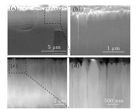
Fig. 6. (a) Cross-sectional SEM images of sample S4, (b) the magnified SEM images of the dashed rectangle in(a). (c)Cross-sectional TEM images of sample S4,(d)the magnified TEM images of the dashed rectangle in(c).
4. Conclusion
The influences of growth condition on surface morphology, residual strain and crystalline quality of AlN films have been investigated. Porous AlN films grown on C-face SiC by HVPE can be obtained on medium V/III. Porous AlN films can grow to 8 μm without cracks, and the crystal quality is improving with the increase of thickness.The characterization of cross-sectional SEM and TEM images show that the pores on the surface of aluminum nitride film are actually V-shaped pits. The bottom of each pit is connected with a microtubule penetrating the film. This discovery may have important value for the preparation and application of porous AlN materials.
猜你喜欢
杂志排行

Chinese Physics B的其它文章
- Real non-Hermitian energy spectra without any symmetry
- Propagation and modulational instability of Rossby waves in stratified fluids
- Effect of observation time on source identification of diffusion in complex networks
- Topological phase transition in cavity optomechanical system with periodical modulation
- Practical security analysis of continuous-variable quantum key distribution with an unbalanced heterodyne detector
- Photon blockade in a cavity–atom optomechanical system