PbI2/Pb5S2I6 van der Waals Heterojunction Photodetector
2022-08-08ZHOUXinCHENJiayuan陈家媛WANGChunrui王春瑞
ZHOU Xin(周 鑫),CHEN Jiayuan(陈家媛),WANG Chunrui(王春瑞)
College of Science, Shanghai Institute of Intelligent Electronics and Systems, Donghua University, Shanghai 201620, China
Abstract: Investigations of two-dimensional(2D)/one-dimensional(1D)van der Waals(vdW)heterojunctions have attracted significant attention due to their excellent properties such as the smooth heterointerface, the highly gate-tunable bandgap, and the ultrafast carrier transport. However, the complicated method of manufacturing vdW heterojunction represents a major problem that severely limits their practical applications. Herein, we develop one-step hydrothermal method and use it to synthesize 2D PbI2/1D Pb5S2I6 vdW heterojunction. The PbI2/Pb5S2I6 vdW heterojunction photodetector(PD)displays lower dark current(<20 pA), higher responsivity(up to 134 mA·W-1), self-powered and wider response spectrum in comparison with that of pristine PbI2 PD and Pb5S2I6 PD. This one-step hydrothermal method provides a new idea for preparing other mixed-dimensional heterojunction.
Key words: one-step hydrothermal method; van der Waals(vdW)heterojunction; photodetector(PD); self-powered; lower dark current; responsivity
Introduction
Thanks to the early separation of graphene, the technology of photodetector(PD)construction methods based on two-dimensional(2D)layered van der Waals(vdW)materials has made considerable progress.The 2D layered vdW material family is growing, such as transition metal dihalides(MoS2[1-3], WSe2[4-6], MoTe2[7-9], SnS2[10-13], SnSe2[14-15],etc.), black phosphorus(BP)[16-18], insulators(e.g.boron nitride(BN)[19-21]).Since the chemical bonds on the surface are completely saturated, the interactions between the adjacent layers of 2D layered materials(2DLMs)are usually characterized by vdW forces[22-23].In the absence of direct chemical bonds, the vdW interaction can ignore the lattice matching problem and directly integrate various materials.It makes great freedom in integrating vdW heterojunction devices based on different 2DLMs, which is superior to the traditional methods.VdW heterojunction can be integrated into nanomaterials of different dimensions, including the 2DLMs/0D[24-27](e.g.nanoparticles and quantum dots(QDs))and 2DLMs/1D nanomaterials[5, 28-31](such as nanowires and nanotubes).In existing reports, the design and construction of vdW heterojunction devices provide a new way for the integration of hybrid vdW heterojunction in the future.Although they work in many unique devices, such as broadband PDs with ultra-high speed or high gain, and a new generation of atomic thin transistors with unprecedented speed and flexibility.But they all have some problems in the construction of the device.For example, the earliest vdW heterojunction graphene and BN[32], needed to be mechanically peeled off and then mechanically combined together to form a vdW heterojunction.There were many similar reports about this mechanical peeling construction method.Liuetal.[33]reported a Bi2O2Se/BP vdW heterojunction device, which was constructed by stacking BP thin flake on top of 2D Bi2O2Se thin flake.The 2D Bi2O2Se flake was synthesized on a mica surface by chemical vapor deposition(CVD)methods and transferred onto a 300 nm SiO2/Si substrate using the poly methyl methacrylate(PMMA)-mediated method.Then use polydimethy-lsiloxane(PDMS)as a support matrix to transfer the BP flakes to the Bi2O2Se flake.Sunetal.[34]reported an optical memory device based on MoS2/QDs vdW heterojunction, which was constructed by stacking QDs on top of a single layer 2D MoS2thin.A triangular monolayer MoS2grown by CVD method[35]is transferred to the SiO2/p++Si substrate as a conducting channel.In this structure, p++Si can be used as the bottom gate electrode and source/drain electrodes are patterned by electron beam lithography to deposit 5 nm Cr and 50 nm Au.Afterwards, CdSe/ZnS core-shell QDs dispersed in toluene solution with a concentration of 25 mg·mL-1.The mixed solution is spin-coated onto the MoS2surface and then treated by a ligand exchange process[36].Afzaletal.[37]manufactured a field effect transistor with excellent performance based on MoTe2/PdSe2vdW heterojunction.In this work, in order to fabricate the MoTe2/PdSe2vdW heterojunction, multilayer PdSe2nanoflakes are transferred to the top of a PDMS stamper by the mechanical exfoliation method.Next, the nano flakes with multiple layers of PdSe2on the PDMS stamper are transferred to the multilayer MoTe2flakes preparing on the Si/SiO2substrate through a micro aligner.Subsequently, the MoTe2/PdSe2vdW heterojunction was placed in a furnace for thermal annealing at 200 ℃ under the flow of hydrogen and argon mixed gas.The argon content is 97.5% and the hydrogen content is 2.5%.Many similar vdW heterojunction devices can be made by this mechanical method[38-43].Unlike the former, Shawkatetal.[44]studied a near-to-mid infrared photodetection based on PtTe2/Si vdW heterojunction.In this method, the vdW heterojunction framed by electron-beam evaporation(Thermionics VE-100, America).Minetal.[45]processed a method for epitaxial growth of large Ga2O3film, which required a multi-step growth method in the experiment including epitaxial growth and pulsed laser.Zengetal.[46]used experimental methods such as photolithography and magnetron sputtering to construct a vdW heterojunction and fabricate a PtTe2/Si vertical Schottky junction PD.
Due to these excellent properties, the 2D layered vdW materials have attracted great attention in the process of synthesis and mixed size assembly.Undesirably, most construction methods are realized by mechanical peeling and multi-step experimental methods.Therefore, the development of a simple one-step method to fabricate vdW heterojunction is necessary and urgent and challenging.
The purpose of this study is to fabricate vdW heterojunction by simple one-step hydrothermal method.Based on our group’s previous research on the construction of PbI2/SbSI heterojunction and the hydrothermal synthesis of PbI2and Pb5S2I6[47-49], we develop one-step hydrothermal method and use it to synthesize 2D PbI2/1 D Pb5S2I6vdW heterojunction.The PbI2/Pb5S2I6vdW heterojunction PD displays lower dark current(<20 pA), higher responsivity(up to 134 mA·W-1), self-powered and wider response spectrum in comparison with those of PbI2PD and Pb5S2I6PD.
1 Experiments
1.1 Synthesis and characterization of materials
Based on the previous work of the group, a one-step hydrothermal method is developed to prepare PbI2/Pb5S2I6vdW heterojunction.In a typical procedure, analytical pure lead chloride(PbCl2, 5 mmol), iodine(I2, 8 mmol)and thiourea((NH2)2CS, 1.3 mmol)are added to a Teflon-lined autoclave with a capacity of 60 mL.The autoclave is filled with distilled water up to 80% of the total volume, kept at 150oC for 15 h and then naturally cooled to room temperature.The obtained yellow flakes and red rod-shaped combined products are filtered and washed.Finally, the products are dried in vacuum at 80oC for 3 h.
The morphology of the obtained PbI2/Pb5S2I6vdW heterojunction is determined with a field emission scanning electron microscope(FESEM, Hitachi, S-4800, Japan).The as-synthesized PbI2/Pb5S2I6vdW heterojunction was characterized by powder X-ray diffraction(XRD)measurements recorded with a Rigaku D/max-2550 PC X-ray diffractometer with a rotating anode and a Cu Kα radiation source(Rigaku, λ=0.154 056 nm, Japan).
1.2 Construction and characterization of PD
The schematic illustration of the fabrication process of PbI2/Pb5S2I6vdW heterojunction PDs is shown in Fig.1.First, the device substrate(polyimide(PI))was cleaned with ethanol, acetone, and deionized water(15 min each time).Second, a single PbI2/Pb5S2I6vdW heterojunction is transferred to the substrate with clean tweezers.Then, the silver paste was placed on both ends of the PbI2/Pb5S2I6vdW heterojunction using a probe with a tip diameter of about 1 μm, while ensuring that the silver paste electrode does not cover the contact part of PbI2/Pb5S2I6vdW heterojunction.Finally, the prepared device is placed in a blow-drying oven at 80oC for 2 h.
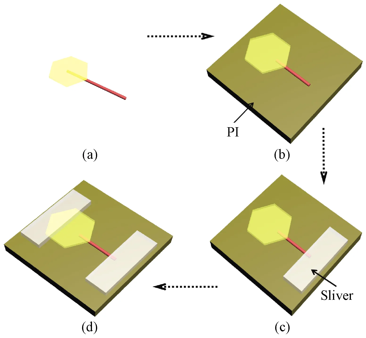
Fig.1 Schematic illustration of the fabrication process of PbI2/Pb5S2I6 vdW heterojunction PDs:(a)PbI2/Pb5S2I6 vdW heterojunction;(b)transfer the sample on the PI substrate;(c)make the silver electrode;(d)schematic diagram of the device
The semiconductor monitoring analyzer(Keithely-4200, China)is used to measure and characterize the current-voltage(I-V)characteristics of the device.The light source used is 300-900 nm monochromatic light generated by a 300 W xenon lamp and matching grating, and the intensity of the light is measured with a standard silicon photometer.
2 Results and Discussion
2.1 Characterization of PbI2/Pb5S2I6 vdW heterojunction
The scanning electron microscope(SEM)image of the PbI2/Pb5S2I6vdW heterojunction is shown in Fig.2(a).It can be seen that the PbI2/Pb5S2I6vdW heterojunction products are distributed in a fan-like shape.According to the previous work in the group,the fan’s handle part is composed of dark red Pb5S2I6[48], and the fan’s surface part is composed of hexagonal bright yellow PbI2[49].The XRD pattern of PbI2/Pb5S2I6vdW heterojunction in Fig.2(b)indicates that the as-produced is composed PbI2and Pb5S2I6.All the peaks can be indexed hexagonal PbI2(PDF#73-1750)and monoclinic Pb5S2I6phase(PDF#23-0329), respectively.
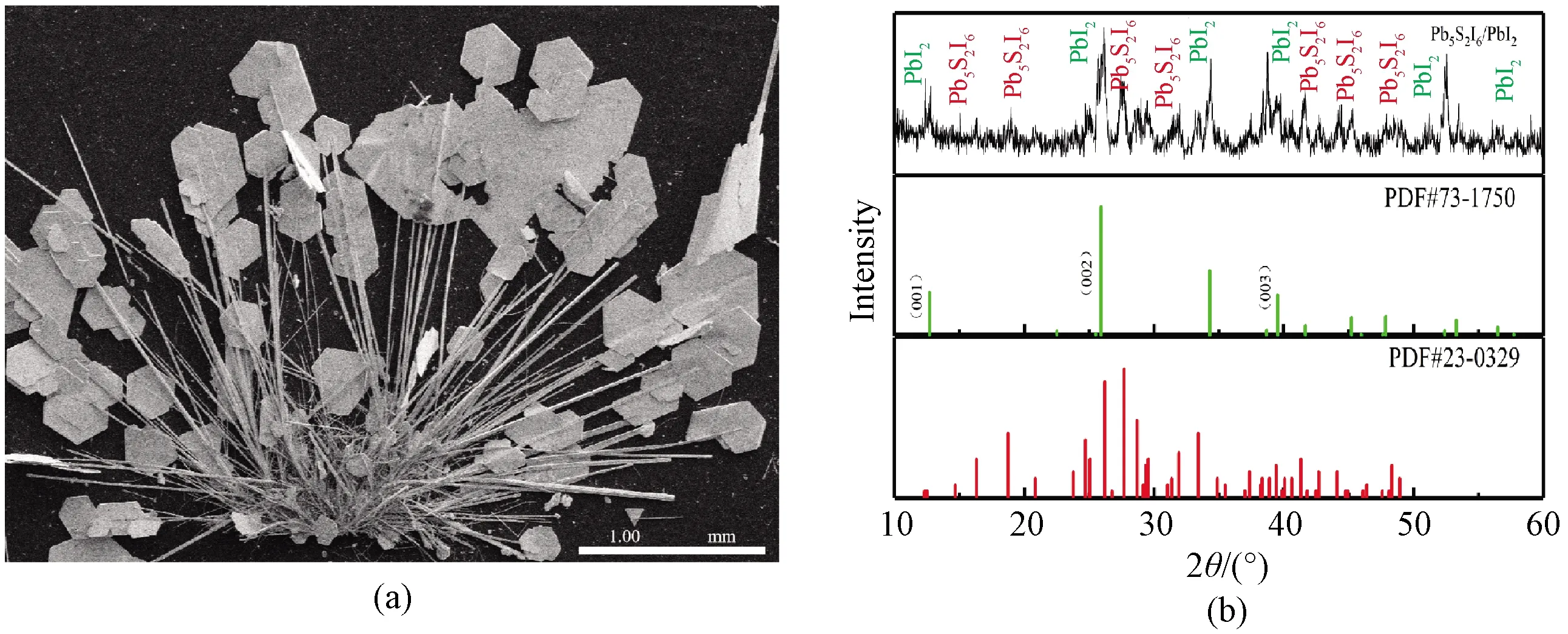
Fig.2 Characterization of PbI2/Pb5S2I6 vdW heterojunction:(a)SEM image;(b)XRD patterns of as-synthesized PbI2/Pb5S2I6 vdW heterojunction
Combined the experimental results and the crystal structure model, the possible mechanism of PbI2/Pb5S2I6vdW heterojunction formation is proposed.During the hydrothermal reaction, PbI2nanoplates[49]and Pb5S2I6nanorods are connected together due to collision-induced aggregation[50].From the SEM image, XRD pattern, it can be seen that the PbI2is oriented(00 l)crystal planes.The terminal of(00 l)crystal plane corresponds to the Pb atomic layer on the surface of the PbI2, as shown in Fig.3(a).The lower crystal plane of one-dimensional Pb5S2I6is also(00 l), and the terminal surface is a layer of Pb atoms and S atoms(shown in Fig.3(a)).So,(00 l)plane of Pb5S2I6nanorods is epitaxially grown on(00 l)plane of PbI2nanoplates(shown in Fig.3(b))due to the suspending bonds of Pb5S2I6and PbI2(shown in Fig.3(a)), and with the aid of HI from disproportionated reaction of I2during the hydrothermal process[48].The mechanism for collision-induced aggregation and growth of home structure under hydrothermal conditions, considering the primary nanoparticles in suspension as molecules, has been described in literatures in the last decade.Xueetal.[50]described the kinetics of oriented aggregation proposing the existence of a rapid equilibrium for the association/dissociation of nanocrystals and an irreversible conversion of associated nanocrystals for producing oriented aggregates.So PbI2/Pb5S2I6vdW heterojunction(shown in Fig.3(c))can be formed on basis of primary PbI2nanoplate and Pb5S2I6nanorod as a template.
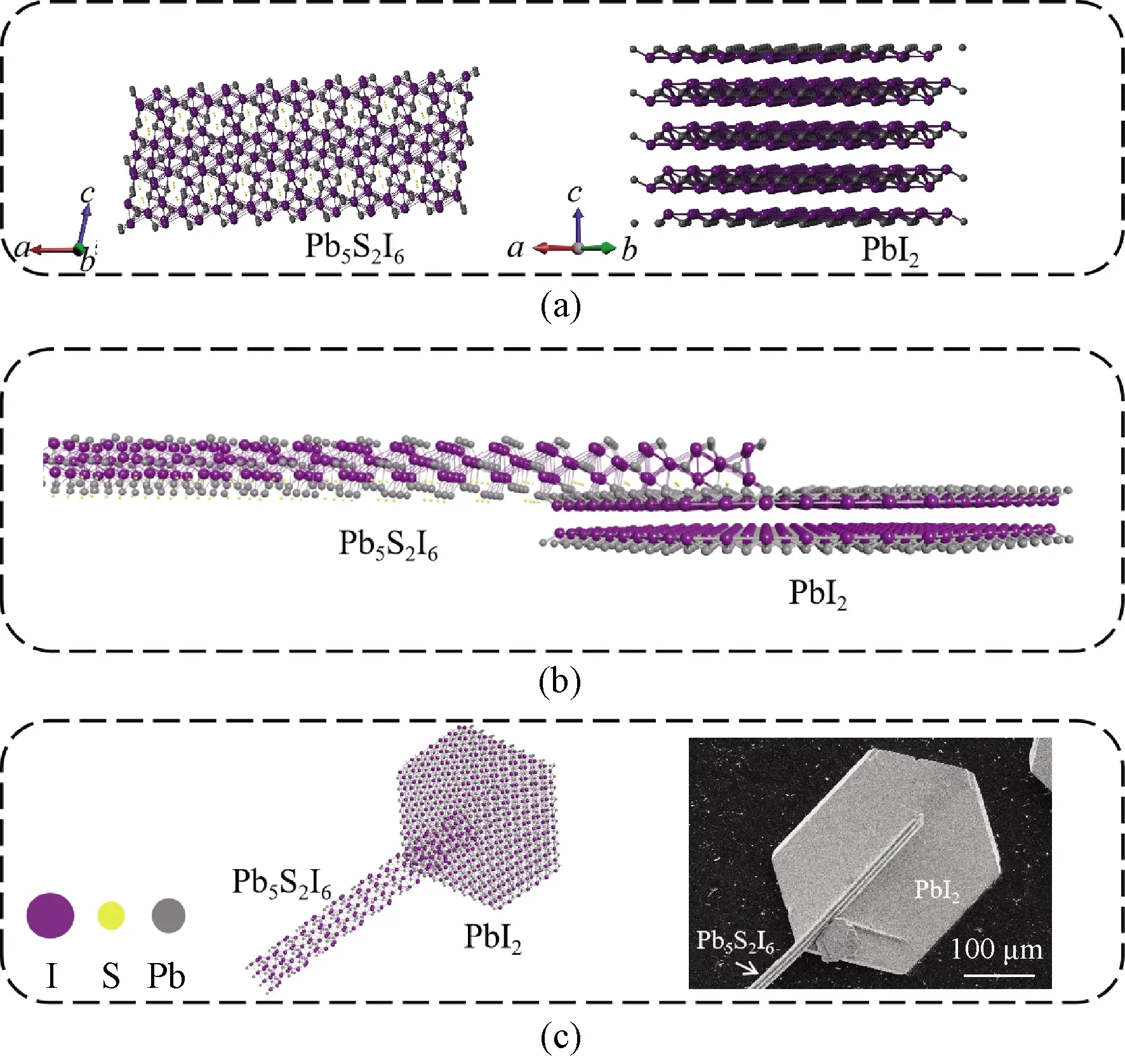
Fig.3 Schematic diagram of the formation mechanism of PbI2/Pb5S2I6 vdW heterojunction:(a)crystal structure of Pb5S2I6 and PbI2;(b)epitaxial relationship between(00l)plane of Pb5S2I6 and PbI2;(c)SEM image of PbI2/Pb5S2I6 vdW heterojunction
2.2 Performance analysis of PD based on PbI2/Pb5S2I6 heterojunction
In order to further study the photoelectric properties of PbI2/Pb5S2I6vdW heterojunction PDs.The schematic diagram of PbI2/Pb5S2I6vdW heterojunction PD is shown in Fig.1(d).The I-V curve of the light and dark current of the device is shown in Fig.4, indicating that the wavelength is continuously increased to 600 nm, and the current firstly increase and then decrease.There is a large photocurrent response in range of 510 nm-560 nm at bias voltage of 5 V.The PbI2/Pb5S2I6vdW heterojunction present a wider response from 300 nm to 600 nm and the highest responsivity up to 134 mA·W-1at 525 nm, which is higher than that of pristine PbI2PD and Pb5S2I6PD[49].
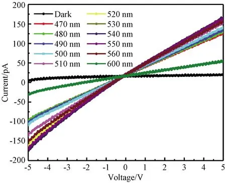
Fig.4 I-V curve of PD based on PbI2/Pb5S2I6 vdW heterojunction under dark and different wavelength conditions
The photo-switching current of PbI2/Pb5S2I6vdW heterojunction PD verse time under varied full wavelength incident light illuminations at 0 V bias is illustrated in Fig.5(a).It can be seen that the ratio of light current to dark current is about 2, implying that the PD present a self-powered property[51].One cycle of photo-switching photocurrent under illumination of 525 nm at 0 V with the rise time and recovery time of 58 ms respectively is displayed in Fig.5(c).Here, the rise time is defined as the photocurrent from 10% to 90% of the peak value and the recovery time is defined as the photocurrent from 90% to 10% of the peak value[52].For comparison, the photo-switching current and corresponding one cycle of photo-switching photocurrent verse time under illumination of 525 nm at bias voltage of 5 V is shown in Figs.5(b)and 5(d), respectively.Although the photo-switching property of the latter is superior to that of the former, the rise time and recovery time of the latter is same as the former.Comparison of performance parameters of different PDs based on PbI2, Pb5S2I6,and PbI2/Pb5S2I6vdW heterojunction are listed in Table 1[53-54,49].The fabricated PbI2/Pb5S2I6vdW heterojunction PD has a fast response speed, and a higher responsivity.It is worth mentioning that the method of preparing PbI2/Pb5S2I6vdW heterojunction is one-step hydrothermal method, which is simple and low-cost.
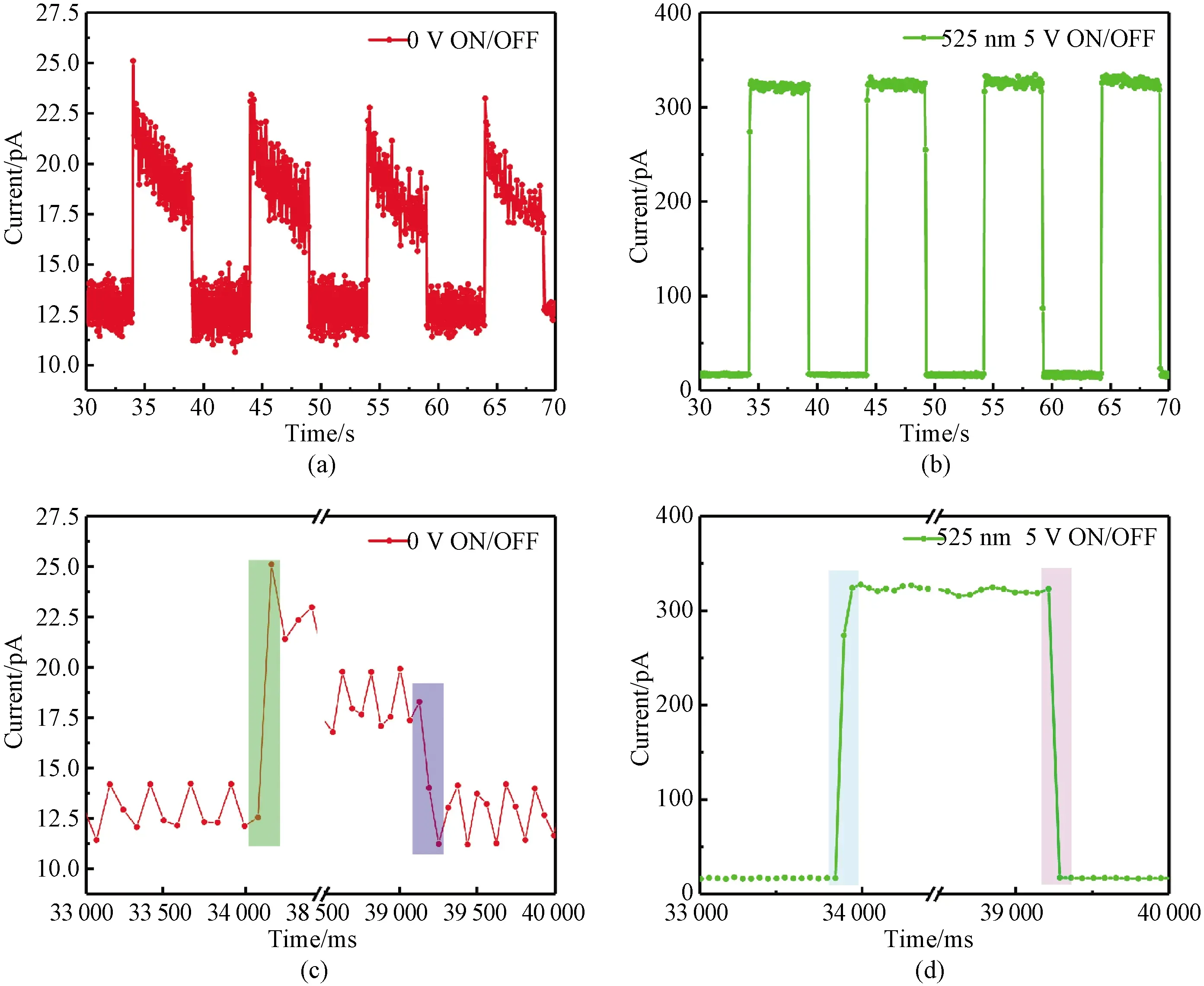
Fig.5 Photo-switching response of PbI2/Pb5S2I6 vdW heterojunction PDs:(a)optical switch response of the device at 0 V bias;(b)optical switch response of the device under the excitation of 525 nm optical wavelength at 5 V bias;(c)-(d)correspond to the rise and fall time of the light switch in(a)and(b),respectively, the time of the rise and fall are 58 ms
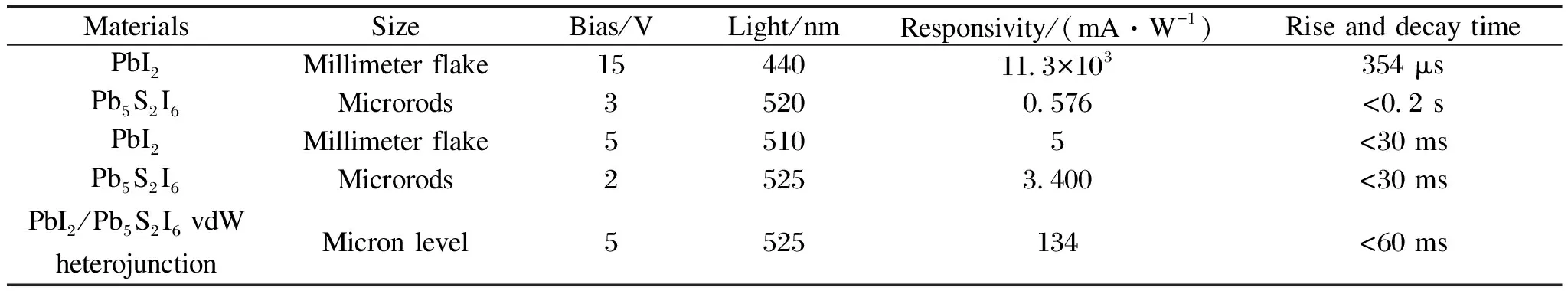
Table 1 Comparison of performance parameters of different PDs based on PbI2, Pb5S2I6 and PbI2/Pb5S2I6 vdW heterojunction
The possible working mechanism of present self-powered PD was proposed on the basis of energy band diagram as shown in Fig.6.A built-in potential barrier exists across PbI2/Pb5S2I6vdW heterojunction(shown in Fig.6(a))and alters the energy band.The photo-generated electron and holes are separated by the built-in potential barrier(shown in Fig.6(b)), leading to the formation of net photocurrent in the external circuit without external power supply, which is similar to the separation of photo-generated electron and holes inp-njunction.This self-powered phenomenon is observed in 1D/2D heterojunction PDs[5, 29, 55].When light is illuminated, the contact part of the junction generates photo-generated carriers.
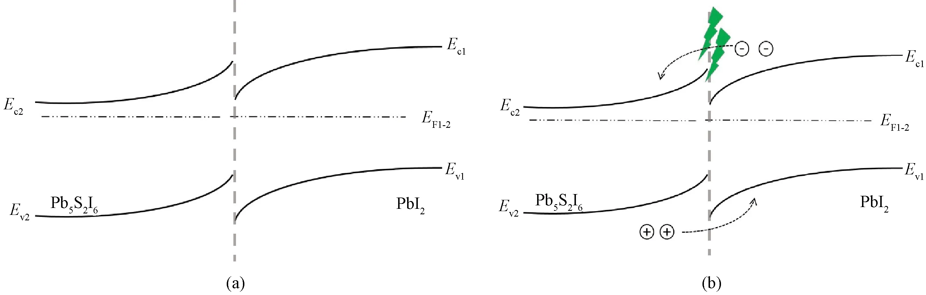
Fig.6 Energy band diagram of PbI2/Pb5S2I6:(a)changes in energy band after contact;(b)carrier transfer in energy band under 0 V bias with the light on conduction band(Ec),valence band(Ev)and Fermi level(EF)
For comparison, Fig.7 shows spectral response and dark current at two different bias voltage of PbI2/Pb5S2I6vdW heterojunction, pristine PbI2PD, and Pb5S2I6PD.It can be seen that the PbI2/Pb5S2I6vdW heterojunction PDs has a wider response range in comparison with that of PbI2, which may attribute to a broad response of Pb5S2I6[49], Pb5S2I6can effectively improve the spectral response effect of PbI2/Pb5S2I6vdW heterojunction PDs.The dark currents of PDs with three configurations under different bias voltages(1 V and 5 V)are compared as shown in Figs.7(c)and 7(d).PbI2/Pb5S2I6vdW heterojunction PD has lower dark current in comparison with that of pristine PbI2PD and Pb5S2I6PD.The built-in potential barrier exists across PbI2/Pb5S2I6vdW heterojunction(shown in Fig.6(a)), which may lead to the lower dark current.It is analogous to the principle ofp-njunction dark current.Inside thep-njunction, there are more electrons in thenregion and more holes in thepregion.At this point, the internal electric field of thep-njunction will prevent this diffusion and thus reduce the dark current.The lower dark current means that vdW heterojunction PDs have the ability to detect weak light intensities.The similar case has been observed in other 2D-based vdW heterojunction PD[49, 56-58].
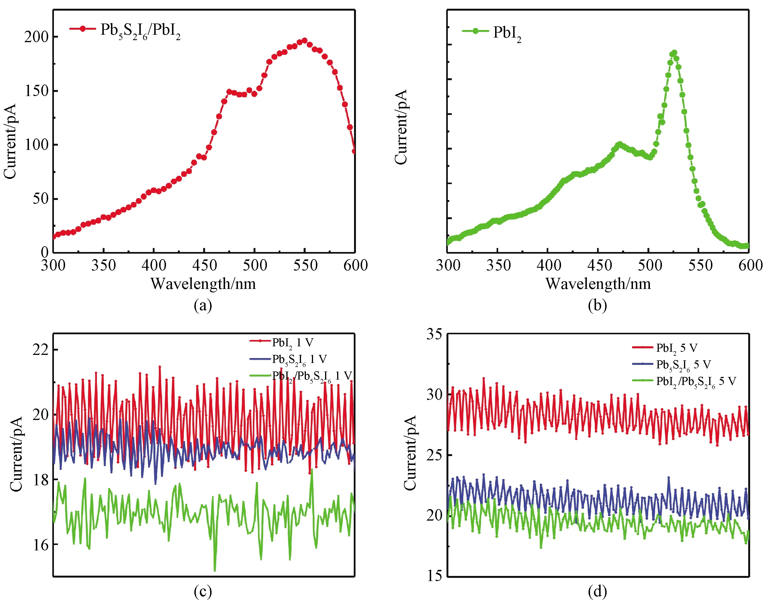
Fig.7 Comparison test results of PD under PbI2, Pb5S2I6, and PbI2/Pb5S2I6 vdW heterojunction:(a)spectral response of PbI2/Pb5S2I6 vdW heterojunction;(b)spectral response of PbI2;(c)-(d)dark current comparison of the optical detector of the three structures at 1 V and 5 V biases
3 Conclusions
In summary, the PbI2/Pb5S2I6vdW heterojunction is successfully synthesized by one-step hydrothermal method.The PbI2/Pb5S2I6vdW heterojunction PD exhibits a responsivity of up to 134 mA·W-1at 525 nm, a low dark current(<20 pA), self-powered and wide response spectrum, which is superior to the pristine PbI2PD and Pb5S2I6PD.The present study may shed light on fabricating other series of mixed-dimensional vdW heterojunction.
猜你喜欢
杂志排行

Journal of Donghua University(English Edition)的其它文章
- Three-Dimensional Model Reconstruction of Nonwovens from Multi-Focus Images
- Toughness and Fracture Mechanism of Carbon Fiber Reinforced Epoxy Composites
- Three-Dimensional Metacomposite Based on Different Ferromagnetic Microwire Spacing for Electromagnetic Shielding
- Blockchain-Based Architectural Framework for Vertical Federated Learning
- Optimal Control of Heterogeneous-Susceptible-Exposed-Infectious-Recovered-Susceptible Malware Propagation Model in Heterogeneous Degree-Based Wireless Sensor Networks
- Enhanced Arsenite Removal Using Bifunctional Electroactive Filter Hybridized with La(OH)3