Temperature-Dependent Growth of Ordered ZnO Nanorod Arrays
2022-05-09ZHANGLiangwei张梁唯YANYali严雅丽WANGJiale王佳乐
ZHANG Liangwei(张梁唯), YAN Yali(严雅丽), WANG Jiale(王佳乐)
College of Science, Donghua University, Shanghai 201620, China
Abstract: Ordered ZnO nanorod arrays were epitaxially grown on GaN substrates by a hydrothermal method. The patterned template was made by transferring a self-assembled close-packed monolayer of polystyrene (PS) nanospheres onto GaN substrates. Then magnetron sputtering of SiO2 was used to mediate the size of PS nanospheres by plasma etching and form periodic seed sites for the following ZnO growth. It was observed that the size of ZnO nanorods could be varied by changing the temperature of hydrothermal growth, and the relationship between height and diameter of nanorods versus growth temperature was studied. This work provides a potential low-cost hydrothermal method for the preparation of ordered semiconductor nanorod arrays.
Key words: ZnO; nanorod array; hydrothermal method; size regulation
Introduction
Due to quantum confinement, nanorods display a lot of unique properties,e.g.high quantum efficiency, direct electron transfer pathways, and enhanced photoelectric conversion efficiency[1-4]. Thus nanorods have been extensively studied as potential materials for the new electronic and optical devices with higher efficiency and lower cost[5-7]. Recently, ordered nanorod arrays, which present a higher light absorption efficiency than nanorod arrays without periodic structures[8-9], arouse much interest. Meanwhile, it has been reported that ordered nanorod arrays can improve the performance of devices[10-13].
ZnO, due to its excellent photoelectric properties[14], superior mechanical and thermal stability[15], wonderful piezoelectric properties[16], and good biocompatibility[17], has been used in various areas,e.g.sewage treatment[18], dye-sensitized solar cells[19], field-effect transistors[20], and sensors[21]. Moreover, nanoscaled ZnO demonstrates some new properties and thus has been widely investigated in the last decades. For example, Cheluetal.[22]reported that ZnO nanostructures on flexible substrates could reach a piezoelectric coefficient about 4 times higher than that on rigid substrates. Akhavanetal.[23]found that ZnO nanorod arrays had an excellent ultraviolet-induced photocatalytic antibacterial effect. Liuetal.[24]reported that ultraviolet LEDs made of ordered high-density ZnO nanowire arrays displayed about 3 times higher maximum luminance than that of disordered nanowire arrays. Wangetal.[25]developed an ultrasonic-driven ZnO nanorod array nanogenerator which could provide power to drive nanosystems and nanodevices.
GaN is a wurtzite semiconductor material with lattice constants ofa=0.318 nm andc=0.518 nm[26]. The lattice mismatch between ZnO (a=0.325 nm, andc=0.521 nm) and GaN is only about 2 %, and thus GaN is selected as the substrate for epitaxial growth of ZnO nanorod arrays. In order to realize ordered arrays, a good patterned template formed on substrates is necessary to limit the growth of ZnO. Here, nanosphere lithography (NSL), an efficient and low-cost technology for large-scale periodic structures, is used to fabricate patterned template. Firstly, polystyrene (PS) nanospheres are used to self-assemble a close-packed monolayer on the surface of water, and then the monolayer of PS nanosphere is deposited on a GaN substrate. Subsequently, radio frequency (RF) magnetron sputtering of SiO2is used to reduce the size of PS nanospheres by plasma etching and transfer the pattern to the substrate. After removing the PS nanospheres, periodic seed sites are accomplished for the following ZnO growth. Finally, the hydrothermal method is used for the growth of ZnO nanorods. The relationship between morphological characteristics of ZnO versus growth temperature is explored. This work provides a potential low-cost hydrothermal method for the fabrication of ordered semiconductor nanorod arrays.
1 Experiments
1.1 Materials and instruments
PS suspension (Duke 5050A, mass fraction of 10%) was purchased from ThermoFisher. Hexamethylenetetramine (HMTA) [C6H12N4, analytical reagent (AR), Hushi, China], triton X-100 [(C2H4O)n·C14H22O, ≥98%, Adamas, China], Tetrahydrofuran (C4H8O, AR, Hushi, China) and zinc nitrate hexahydrate [Zn(NO3)2·6H2O, ≥99%, Adamas, China] were used without any further purification. Deionized (DI) water (18.2 MΩ) was used throughout the experiments.
The scanning electron microscopy (SEM) images were obtained by Hitachi S-4800 field-emission scanning electron microscopy (FESEM, Hitachi, Japan). X-ray diffraction (XRD) characterization of the sample was performed by a Rigaku D/Max-2550 (Rigaku, Japan). X-ray photoelectron spectroscopy (XPS) was carried out using an ESCALAB 250Xi (Thermo Fisher Scientific, USA) with monochromatic Al Kα (1 486.7 eV). High resolution transmission electron microscopy (HRTEM) images were obtained by a TECHAI G2S-TWIN (FEI, USA).
1.2 Fabrication of ZnO nanorod arrays
GaN epitaxy on (0001) sapphire substrate was cleaned by acetone, ethanol and DI water in turn using an ultrasonic cleaner. Glass slide was immersed in piranha solution (volume ratio, H2O2∶H2SO4=3.0∶7.0) for 10 min to obtain a hydrophilic surface. Active agent of PS nanospheres was prepared by dissolving 0.162 g Triton X-100 in 250 mL DI water and the solution was heated at 30 ℃ for 4 h.
The monolayer of PS nanospheres was prepared following the method of Weekesetal.[27]. Briefly, 6 mL DI water was poured into a plastic petri dish, where a glass slide treated by piranha solution was leaned on its side wall and a GaN substrate was put on the bottom. Then 10 drops of active agent were slowly added to the DI water along the edge of the petri dish. The PS suspension was diluted with ethanol in a ratio of 1.0∶2.5, and the diluted PS suspension was slowly dropped onto the glass slide. A monolayer of PS nanospheres was self-assembled when the PS suspension slid down and touched the surface of water. Afterwards, DI water was slowly drawn out, and the monolayer of PS nanospheres was deposited on the GaN substrate.
Then RF magnetron sputtering of SiO2was carried out at 20 W plasma power for 20 min. The base pressure was about 2 Pa. After removing the PS nanospheres by tetrahydrofuran, a GaN substrate with periodic seed sites was accomplished for the following ZnO growth.
Finally, ZnO nanorod arrays were grown on the patterned GaN substrates in a Teflon-lined stainless steel autoclave with 1.486 g Zn(NO3)2·6H2O and 0.700 g HMTA dissolved in 100 mL DI water. The reaction was carried out for 6 h at temperature of 55, 60, 65, and 70 ℃, respectively. When the autoclave was cooled to room temperature, the substrates were taken out and cleaned with ethanol and DI water in turn. And then the substrates were dried at 50 ℃.
2 Results and Discussion
2.1 Morphology of ZnO nanorod arrays
Figure 1(a) shows the SEM images of a monolayer of close-packed PS nanospheres on a GaN substrate, which is self-assembled on the surface of water and then deposited on the GaN substrate. Subsequently, RF magnetron sputtering of SiO2was used to reduce the size of PS nanospheres and transfer the pattern to the substrate. As shown in Fig. 1(b), the PS nanospheres still maintain good periodicity after the sputtering. The interstitial space among the PS nanospheres is covered by SiO2, which can prevent the growth of ZnO there. After removing the PS nanospheres, periodic seed sites were accomplished for the following ZnO growth.
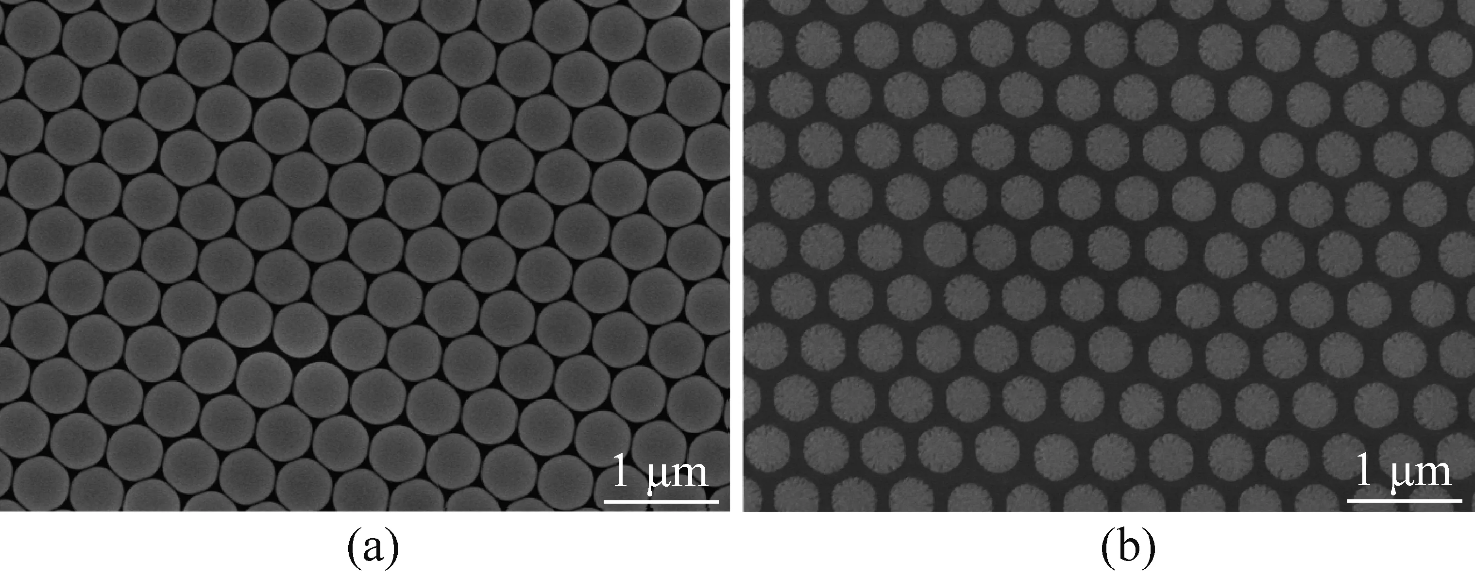
Fig. 1 SEM images of self-assembled PS nanosphere monolayer with close-packed structure: (a) before and (b) after RF magnetron sputtering of SiO2
It has been reported that various factors,e.g.growth solution concentration, growth time, and pH value, can affect the growth of ZnO nanorod arrays[28]. However, the influence of growth temperature on ZnO nanorod arrays has not been studied. Figure 2 shows the morphology of ZnO nanorod arrays grown at 55, 60, 65 and 70 ℃, respectively, where the SEM images are taken with three angles of 90° [Figs. 2(a), 2(d), 2(g), and 2(j)], 45° [Figs. 2(b), 2(e), 2(h), and 2(k)] and 0° [Figs. 2(c), 2(f), 2(i), and 2(l)] relative to substrate. The ZnO nanorods are hexagonal and grow perpendicular to the substrate, and the size is relatively uniform. The average height of ZnO nanorods is 185 nm at 55 ℃, 275 nm at 60 ℃, 385 nm at 65 ℃, and 600 nm at 70 ℃, respectively, while the diameter is 342 nm at 55 ℃, 372 nm at 60 ℃, 414 nm at 65 ℃, and 430 nm at 70 ℃, respectively. Thus it demonstrates that the size of ZnO nanorods increases with growth temperature, and the relationship is plotted in Fig. 3. Meanwhile, the nanorod arrays display a periodic characteristic as the seed sites on patterned substrate.
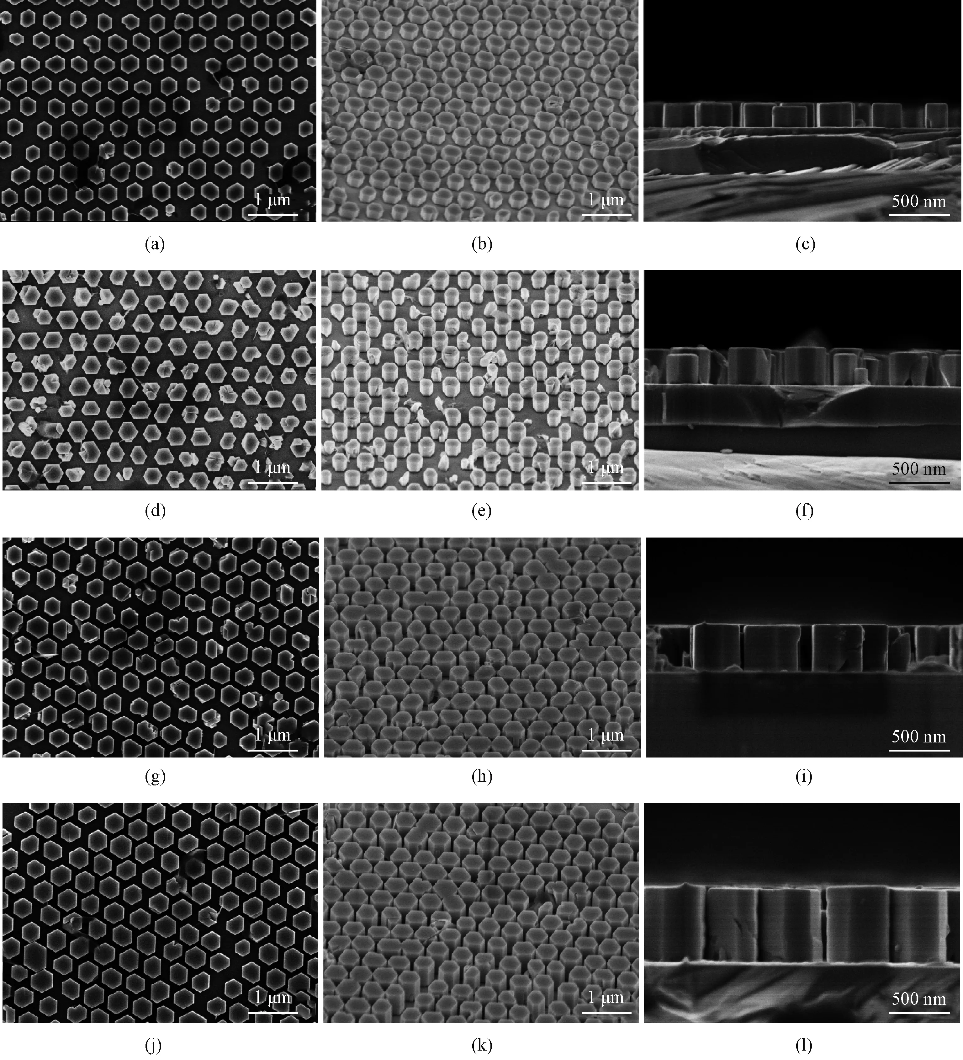
Fig. 2 SEM images of ZnO nanorod arrays grown at (a)-(c) 55 ℃; (d)-(f) 60 ℃; (g)-(i) 65 ℃; (j)-(k) 70 ℃ with 90°, 45°, and 0° relative to substrate

Fig. 3 Relationship between height and diameter of ZnO nanorods versus growth temperature
However, as shown in Fig. 4, when the temperature reaches 75 ℃, incomplete growth can be observed, where the diameter shrinks on the top of ZnO nanorods.
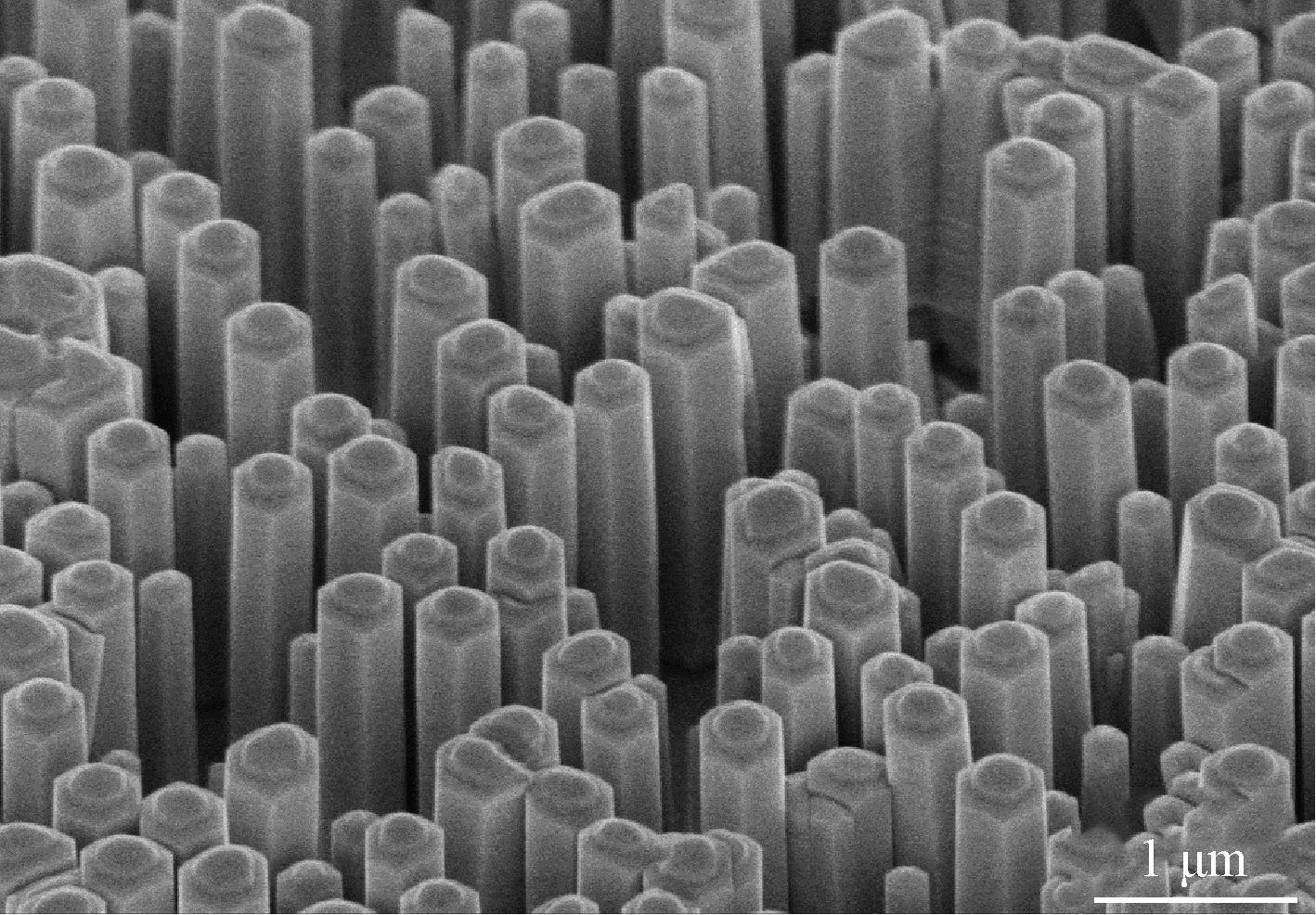
Fig. 4 SEM image of ZnO nanorod arrays grown at 75 ℃ with 45° relative to substrate
2.2 Microstructure characterization of ZnO nanorod arrays
ZnO nanorod arrays grown at 70 ℃ demonstrated superior morphology, which were chosen for microstructure characterization by XRD and TEM. Figure 5 presents the XRD pattern of this sample. There are five peaks observed on the pattern. The peaks at 34.40° and 72.81° correspond to the (0002) and (0004) crystal planes of ZnO, respectively. The other three peaks at 34.77°, 41.71°, and 73.03° correspond to GaN (0002), Al2O3(0006) and GaN (0004) crystal planes, respectively, coming from the GaN epitaxy on sapphire substrates. It is noted that except (0002) and (0004) crystal planes no other signal corresponding to ZnO is observed, which demonstrates that all the ZnO nanorods grow along [0001] crystal direction.
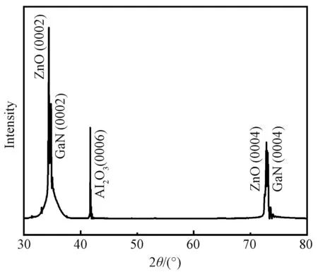
Fig. 5 XRD pattern of ZnO nanorod arrays grown at 70 ℃
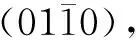
Fig. 6 Microstructure characterizations of ZnO nanorods grown at 70 ℃: (a) TEM image; (b) HRTEM image; (c) SAED image
2.3 Chemical and electronic structure of ZnO nanorod arrays
XPS was also performed on the ZnO nanorod arrays sample grown at 70 ℃ with superior morphology to determine the chemical and electronic structure. Figure 7(a) shows the XPS survey spectrum of ZnO nanorod arrays after calibration using C 1s peak at 284.60 eV. With around 10 min exposure under ultraviolet (UV) irradiation, surface C contamination has an about 14 times minor intensity relative to that of Zn 2p3/2. The Zn 2p3/2core-level spectrum is shown in Fig. 7(b). It can be clearly seen that there are two components with different binding energies (BEs). The main peak labeled I with BE of 1 021.55 eV corresponds to the bulk-coordinated Zn, and the other peak labeled II with low BE of 1 019.06 eV corresponds to reduced Zn, which is known to occur as a result of the formation of oxygen vacancies[30-31]. Figure 7(c) shows the O 1s core-level spectrum and it has three components. Peak I with BE of 530.15 eV corresponds to oxygen of a bulk structure. The peaks labeled II (BE of 531.41 eV) and labeled III (BE of 532.35 eV) are attributed to surface component and chemically carbonate or hydroxyl groups on the surface, respectively[32-33]. The ratio of peak II to peak I presents a larger proportion than that of the ZnO film, which could be attributed to the larger surface-to-volume ratio of nanorod structures[34].
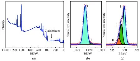
Fig. 7 XPS survey spectra: (a) ZnO nanorod arrays; (b) core-level spectrum of Zn 2p3/2 ; (c) core-level spectrum of O 1s
3 Conclusions
In summary, ordered ZnO nanorod arrays were epitaxially grown on patterned GaN substrates by a hydrothermal method. The patterned GaN substrate with periodic seed sites was obtained by NSL. Firstly, a monolayer of self-assembled close-packed PS nanospheres was deposited on the substrate. Then RF magnetron sputtering of SiO2was used to reduce the size of PS nanospheres by plasma etching and cover the interstitial space between PS nanospheres by SiO2. Finally, the PS nanospheres were removed and periodic seed sites were accomplished on the substrate for the following ZnO growth. The ZnO nanorod arrays are epitaxially grown along [0001] crystal direction and present good crystalline quality. Furthermore, it was observed that the size of ZnO nanorods could be varied by changing the temperature of hydrothermal growth. Thus this work provides a potential low-cost hydrothermal method for the preparation of semiconductor nanorod arrays.
杂志排行

Journal of Donghua University(English Edition)的其它文章
- Electrospinning of Bead-on-String Sodium Alginate Nanofibrous Membrane
- Polysaccharides Based Random and Unidirectional Aerogels for Thermal and Mechanical Stability
- Eco-Friendly pH Indicator Based on Natural Anthocyanins from Lycium ruthenicum
- Formulating Novel Halogen-Free Synergistic Flame Retardant Epoxy Resins for Vacuum Assisted Resin Infusion Composites
- Electrochemical Reduction Determination of N-Nitrosodiphenylamine in Food Based on Graphene Electrode Material
- Hydrothermal Synthesis of Ordered ZnO Nanorod Arrays by Nanosphere Lithography Method