Hydrothermal Synthesis of Ordered ZnO Nanorod Arrays by Nanosphere Lithography Method
2022-05-09YANYali严雅丽ZHANGLiangwei张梁唯WANGJiale王佳乐
YAN Yali(严雅丽), ZHANG Liangwei(张梁唯), WANG Jiale(王佳乐)
College of Science, Donghua University, Shanghai 201620, China
Abstract: Ordered ZnO nanorod arrays were hydrothermally synthesized on a patterned GaN substrate formed by a nanosphere lithography method. Firstly, polystyrene (PS) nanospheres were used to self-assemble a close-packed monolayer on the surface of water. Then the monolayer was transferred onto a GaN substrate. Subsequently, magnetron sputtering of SiO2 was used to reduce the size of PS nanospheres and cover the interstitial space between PS nanospheres by SiO2 at the same time. After removing the PS nanospheres, periodic seed sites were accomplished on the GaN substrate for ZnO growth. Finally, ordered ZnO nanorod arrays, perpendicular to the substrate, were grown on GaN substrates by a hydrothermal method. This work provides a potential low-cost hydrothermal method for the preparation of ordered semiconductor nanorod arrays.
Key words: ZnO; nanorod array; nanosphere lithography(NSL); hydrothermal synthesis
Introduction
Nanorods have been widely investigated in recent decades because of their quantum confinement, which results in various unique properties,e.g.direct transmission channel for charge transport, high quantum efficiency, and reduction of electron-hole recombination rate[1-7]. Moreover, ordered nanorod arrays, which demonstrate some superior properties by enhancing light absorption[8-11], arouse much interest. And ordered nanorod arrays are considered as attractive materials for the new devices with higher efficiency and lower power consumption[12-15]. ZnO nanorods, which present excellent piezoelectric properties, good mechanical capabilities, and outstanding thermal stabilities[16], have been applied in a lot of areas. Wangetal.[17]found that the ZnO ethanol detector displayed a rapid response speed to ethanol at different temperatures. Zhouetal.[18]prepared a single ZnO nanorod strain sensor with excellent stability and fast response, and the detection result presented a linear relationship with the strain. Lawetal.[19]fabricated ZnO nanorod dye-sensitized solar cells, which displayed faster electron injection than ZnO nanoparticles. Societal.[20]reported a ZnO ultraviolet photodetector with extremely high photoconductivity and internal gain. In addition, due to the good biocompatibility of ZnO, it is also utilized in medicine, cosmetics and antibiotics[21-22].
Ordered ZnO nanorods can be fabricated on a patterned template which is generally prepared by photolithography and following etching, and then several methods, such as molecular beam epitaxy (MBE)[23], chemical vapor deposition (CVD)[24], and electrochemical deposition[25], can be used for sample growth. However, here we report preparation of ordered ZnO nanorod arrays by hydrothermal synthesis on patterned substrate formed by nanosphere lithography (NSL). Since GaN (a=0.316 nm, andc=0.513 nm) has a small lattice mismatch (about 2 %) compared with ZnO (a=0.325 nm, andc=0.521 nm)[26-28], it is selected as the substrate for ZnO nanorod arrays growth. Firstly, a monolayer of close-packed polystyrene (PS) nanospheres is self-assembled on the surface of water through the Langmuir-Blodgett method[29], and then it was deposited onto the GaN substrate. Subsequently, radio frequency (RF) magnetron sputtering of SiO2is used to reduce the size of the PS nanospheres by plasma etching, and meanwhile transfer the pattern to the GaN substrate. After the PS nanospheres are removed, a patterned substrate with periodic seed sites is accomplished for the following ZnO growth. Finally, ZnO nanorod arrays are epitaxially grown on the patterned substrate, and it is confirmed by scanning electron microscopy (SEM), X-ray diffraction (XRD) and transmission electron microscopy (TEM) that ZnO nanorods grow perpendicularly to the GaN substrate and along the [0001] crystal direction.
1 Experiments
1.1 Materials and instruments
PS suspension (Duke 5050A, mass fraction of 10%) with a diameter of (500 ± 15) nm was purchased from ThermoFisher. Triton X-114 [(C2H4O)n·C14H22O, ≥98%, Adamas, China], tetrahydrofuran [C4H8O, analytical reagent (AR), Hushi, China], hexamethylenetetramine (HMTA, C6H12N4, AR, Hushi, China) and zinc nitrate hexahydrate [Zn(NO3)2·6H2O, ≥99%, Adamas, China] were used without any further purification. Deionized (DI) water (18.2 MΩ) was used throughout the experiments.
The SEM images were obtained by Hitachi S-4800 field-emission scanning electron microscopy (FESEM, Hitachi, Japan). XRD characterization of the sample was performed by a Rigaku D/Max-2550 (Rigaku, Japan). X-ray photoelectron spectroscopy (XPS) was carried out using an ESCALAB 250Xi (Thermo Fisher Scientific, USA) with monochromatic Al Kα (1 486.7 eV). High resolution transmission electron microscopy (HRTEM) images were obtained by a TECHAI G2S-TWIN (FEI, USA).
1.2 Preparation of GaN substrate with periodic seed sites
GaN epitaxy on (0001) sapphire substrate of 1 cm×1 cm size was thoroughly cleaned by acetone, ethanol, and DI water in turn. Active agent of PS nanospheres was prepared by dissolving 0.647 g Triton X-114 in 1 L DI water, and it was heated at 30 ℃ for 4 h.
The PS suspension was diluted with 2.5 times of ethanol. Quartz glass slide was treated by piranha solution (volume ratio, H2O2∶H2SO4=3∶7) for 10 min. Then it was leaned on the side wall of a petri dish with a GaN substrate on the bottom, and DI water was added. After 30 drops of active agents were added to the petri dish by a 1 mL syringe, the diluted PS suspension was slowly dropped onto the glass slide. When the PS suspension slowly slid down and touched the surface of water, a film of PS nanosphere monolayer was self-assembled. Subsequently, DI water was slowly drawn out, and the film was deposited on the GaN substrate.
Then RF magnetron sputtering of SiO2was carried out at 30 W plasma power for 30 min. The base pressure was about 2 Pa.
Finally, tetrahydrofuran was used to remove the PS nanospheres, and a patterned GaN substrate with periodic seed sites was accomplished for the following ZnO growth.
1.3 Hydrothermal growth of ZnO nanorod arrays
Briefly, 1.486 g Zn(NO3)2·6H2O and 0.700 g HMTA were dissolved in 100 mL DI water. The solution was transferred to a Teflon-lined stainless steel autoclave, and the patterned GaN substrate was put into the liner and heated at 55 ℃ for 6 h. When the autoclave was cooled to room temperature, the substrate was taken out and cleaned with ethanol and DI water in turn, followed by drying at 50 ℃.
2 Results and Discussion
2.1 Fabrication procedure of ZnO nanorod arrays
The schematic diagram depicting the experimental procedure of ZnO nanorod arrays fabrication is illustrated in Fig. 1. Since ethanol could reduce the density of PS suspension, making the nanospheres easier to float on water, PS suspension and ethanol were mixed in a ratio of 1.0∶2.5 for use. A monolayer of PS nanospheres was self-assembled on the surface of water, and then it was deposited on a GaN substrate. Figure 2(a) shows the SEM image of PS nanospheres film on the GaN substrate, where PS nanospheres with a close-packed monolayer structure can be clearly observed. In Fig. 2(b), the PS nanospheres display the same close-packed structure as that in Fig. 2(a) after RF magnetron sputtering of SiO2. However, the size of PS nanospheres reduces to about 410 nm in diameter.

Fig. 1 Schematic diagram depicting experimental procedure of ZnO nanorod array fabrication: (a) monolayer of self-assembled PS nanospheres on a GaN substrate; (b) RF magnetron sputtering of SiO2; (c) removal of nanospheres to obtain a patterned seed layer; (d) ZnO nanorod array growth by a hydrothermal method
Since the crystal structure of SiO2is different from that of ZnO, its coverage on the GaN substrate can prevent ZnO nanorods from growing in the interstitial space between PS nanospheres. Meanwhile, RF magnetron sputtering can also etch the PS nanospheres and decrease the size of seed sites for the following ZnO growth. It is observed in Fig. 2(b) that after the plasma etching PS nanospheres present a rough surface.

Fig. 2 SEM images of PS nanosphere monolayer with a close-packed structure: (a) before and (b) after RF magnetron sputtering of SiO2
Dongetal.[30]reported a method to obtain patterned template for periodic ZnO nanorod array growth, where PS nanospheres were etched by O2plasma to reduce the size, and then the patterned seed layer was obtained by spin-coating TiO2sol and filling in the interstitial space between PS nanospheres. In our case, RF magnetron sputtering of SiO2was used to etch, thus reducing the size of PS nanospheres, and cover the interstitial space between PS nanospheres by SiO2in order to form periodic seed sites at the same time.
2.2 Morphology of ZnO nanorod arrays
The SEM images of ZnO nanorod arrays observed with three angles of 90°, 45°, and 0° relative to the substrate are presented in Fig. 3, respectively. Figures 3(a) and 3(b) show that the ZnO nanorods are hexagonal and grow perpendicular to the substrate. The height of ZnO nanorods demonstrates a relatively uniform distribution. The size of ZnO nanorods can be obtained in Fig. 3(c), which is about 280 nm in height and about 290 nm in diameter. Meanwhile, the nanorod arrays display a periodic characteristic, which are consistent with the periodic seed sites on the patterned substrate.
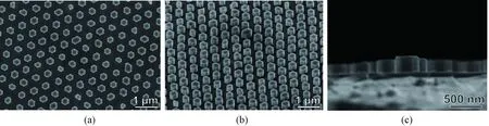
Fig. 3 SEM images of ZnO nanorod arrays with different angles relative to substrate: (a) 90°; (b) 45°; (c) 0°
2.3 Microstructure characterization of ZnO nanorod arrays
Crystal structure of ZnO nanorod arrays is characterized by XRD as shown in Fig. 4. The peaks at 34.40° and 72.81° correspond to the (0002) and (0004) crystal planes of ZnO, respectively. While the peaks at 34.77°, 41.71°, and 73.03° correspond to the GaN (0002), Al2O3(0006) and GaN (0004) crystal planes, respectively, which come from the GaN epitaxy on the sapphire substrate. It is noted that only (0002) and (0004) crystal planes of ZnO are observed, which demonstrates that all the ZnO nanorods grow along [0001] crystal direction.

Fig. 4 XRD pattern of ZnO nanorod arrays

Fig. 5 Microstructure characterizations of ZnO nanorods along the radial direction: (a) TEM image; (b) HRTEM image; (c) SAED image
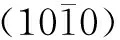
Fig. 6 Microstructure characterizations of ZnO nanorods along the axial direction: (a) TEM image; (b) HRTEM image; (c) SAED image
2.4 Chemical and electronic structure of ZnO nanorod arrays
The XPS survey spectrum of ZnO nanorod arrays is shown in Fig. 7(a). With about 10 min exposure under ultraviolet (UV) irradiation, surface C contamination has about 13 times minor intensity relative to that of Zn 2p3/2. The Zn 2p3/2core-level spectrum in Fig. 7(b) presents two components. The main peak labeled I with binding energy (BE) of 1 021.4 eV corresponds to the bulk-coordinated Zn. The peak labeled II with low BE of 1 018.5 eV corresponds to reduced Zn, which is known to occur as a result of the formation of oxygen vacancies[32]. Figure 7(c) shows O 1s core-level spectrum. The spectrum has three components. Peak I with BE of 530.1 eV corresponds to oxygen in the bulk structure. Peak II (BE of 531.3 eV) and peak III (BE of 532.2 eV) are attributed to surface component and the chemically bound carbonate or hydroxyl groups on the surface, respectively. Compared the intensity of peak II here in O 1s core-level spectrum with that of ZnO film, the peak II of the ZnO nanorod displays a higher proportion, which is due to the larger surface-to-volume ratio of the nanorod structure[33].

Fig. 7 XPS survey spectra: (a)ZnO nanorod arrays; (b)core-level spectrum of Zn 2p3/2; (c)core-level spectrum of O 1s
3 Conclusions
In summary, ordered ZnO nanorod arrays were successfully grown on the patterned GaN substrate by the hydrothermal method. The patterned GaN substrate was fabricated by NSL and following RF magnetron sputtering of SiO2, where the etching of PS nanospheres and the coverage of interstitial space between PS nanospheres by SiO2, could be completed in one step. After removing the PS nanospheres, periodic seed sites were accomplished on the GaN substrate for the following ZnO growth. Moreover, it was shown that the ZnO nanorods were hexagonal and grown perpendicular to the substrate. A series of characterizations such as XRD and TEM confirmed that the ZnO nanorods had a wurtzite crystal structure with good crystal quality. Therefore, the finding might provide a potential low-cost method for fabricating ordered semiconductor nanorod arrays with good crystal quality.
杂志排行

Journal of Donghua University(English Edition)的其它文章
- Electrospinning of Bead-on-String Sodium Alginate Nanofibrous Membrane
- Polysaccharides Based Random and Unidirectional Aerogels for Thermal and Mechanical Stability
- Eco-Friendly pH Indicator Based on Natural Anthocyanins from Lycium ruthenicum
- Formulating Novel Halogen-Free Synergistic Flame Retardant Epoxy Resins for Vacuum Assisted Resin Infusion Composites
- Electrochemical Reduction Determination of N-Nitrosodiphenylamine in Food Based on Graphene Electrode Material
- Temperature-Dependent Growth of Ordered ZnO Nanorod Arrays