High efficiency ETM-free perovskite cell composed of CuSCN and increasing gradient CH3NH3PbI3
2022-01-23TaoWang汪涛GuiJiangXiao肖贵将RenSun孙韧LinBaoLuo罗林保andMaoXiangYi易茂祥
Tao Wang(汪涛) Gui-Jiang Xiao(肖贵将) Ren Sun(孙韧)Lin-Bao Luo(罗林保) and Mao-Xiang Yi(易茂祥)
1School of Microelectronics,Hefei University of Technology,Hefei 230601,China
2School of Electronic Science and Engineering,Southeast University,Nanjing 210096,China
3School of Information Science and Technology,University of Science and Technology of China,Hefei 230027,China
4National Engineering Laboratory of Special Display Technology,Hefei 230009,China
Keywords: electron transporting material(ETM)-free perovskite solar cell,inorganic hole transporting mate
1. Introduction
With high absorption coefficient, long carrier lifetime,high mobility and other good photoelectric characteristics,CH3NH3PbI3has been the subject of extensive research interest recently,and the efficiency of organic-inorganic hybrid perovskite solar cell (PSC) has reached 24.2%.[1]Obviously,the power conversion efficiency (PCE) of PSC is determined by the materials and structures of PSC.[2,3]To explore highperformance PSC,it is of great significance to construct p-i-n or p-n structures by the combination of perovskite and some organic or inorganic materials.
Some performances of p-i-n structure are better than those of n-i-p structure under the same material according to relevant researches, such asJ-Vcurve hysteresis and fill factor.[2-5]A typical inverted planar PSC with p-i-n structure is usually composed of five layers,i.e.,electron transporting material (ETM), hole transporting material (HTM),perovskite absorption material,transparent conducting oxides(TCO),and back electrode. Fullerene(C60, C70)and phenyl-C61-butyric acid methyl ester(PCBM)are the most commonly ETM in p-i-n PSC.[3-6]However, the PCE of the PSC is strictly limited by fullerene and PCBM due to their poor conductivities, multiple pinholes and rough topographies. Moreover, fullerene and PCBM are unstable in ambient condition and expensive due to the complex fabrication process.[6,7]Undoubtedly, these factors seriously hinder the applications of p-i-n PSC with fullerene or PCBM acting as ETM.
Compared with p-i-n PSCs, ETM-free PSC possesses many benefits, such as reduced cost, simplified technology and improved stability. In recent years, the ETM-free PSC has received much attention.[8-13]Inverted ETM-free PSC was fabricated first by Denget al.with ITO-PEDOT:PSSCH3NH3PbI3-Au structure, but the efficiency was only 4.06%.[8]In 2018, PCE of ETM-free PSC was achieved to be 18.1% due to the increased matching of different band gaps materials in ITO-PTAA-MAPbI3-Ti structure.[9]Subsequently, simulation efficiency of ETM-free PSC achieved 22.25% by optimizing the thickness and band offset of materials.[10]Although some ETM-free PSCs have been manufactured, the lack of research on the internal mechanism of PSC hinders the fabrication and application of cell. Furthermore,there are some shortcomings of PEDOT:PSS and PTAA,for instance,they are poor in conductivity,expensive and easily decomposed.[11]
Recently, some inorganic materials with good stability and high mobility have been widely studied,such as CuSCN,CuO, Cu2O, CuI, and NiO.[12,13]However, these materials have not been used to enhance performance of ETM-free PSC so far. Moreover, as a common electrode material for PSC,Au is expensive and there is a Schottky barrier at the Au-CH3NH3PbI3interface. Moreover, the influences of twodimensional electric field,gradient band gap,doping concentration,and bulk defects on the performance of ETM-free PSC have not been reported.
Here in this work, the n-type CH3NH3PbI3, as an absorber, is combined with HTM to form a p-n heterojunction ETM-free PSC. This geometry can form an effective built-in electric field which will allow the photo-generated carriers to be separated under illumination, the carriers to transfer form heterojunction to HTM or n-type CH3NH3PbI3, and the carriers to be collected by the front electrode and the back electrode. Based on TCAD Atlas software, the structural characteristics, material selection, band gap design and some parameters optimization of ETM-free PSC are studied in detail.Some crucial properties,i.e., energy band of heterojunction,two-dimensional distribution of electric field,and recombination rate are characterized.
2. Model calibration and parameters of materials
Since the excitons are of typical Wannier-type in perovskite material, the transport of photogenerated carriers in organic and inorganic materials could be treated with the same method.[14]To ensure the accuracy of the physical model,TCAD simulation of typical plane heterojunction PSC published by Aaeshaet al.[15]is repeated and calibrated. The device structure of Ref. [15] (FTO-TiO2-CH3NH3PbI3-Spiro-OMETAD-Silver) is illustrated in Fig. 1(a). TheJ-Vcharacteristic simulated by our model is compared with that from Ref. [15] as shown in Fig. 1(b). Physical model is calibrated by the two consistentJ-Vcurves. Based on inverted p-in PSCs(HTM-CH3NH3PbI3-ETM),the p-n ETM-free PSCs(HTM-CH3NH3PbI3) are studied and compared with p-i-n PSCs. Schematic structures of two types of PSCs are shown in Figs.1(c)-1(d).

Fig.1. (a)Device structure of PSC in Ref.[15],(b)J-V characteristics,(c)structure of p-i-n PSC,and(d)structure of ETM-free PSC.
The physics parameters of each type of materials that are obtained from the literature[12,14-21]are listed in Table 1,whereεris the relative permittivity,χis the electron affinity,µnandµprepresent mobility of electron and hole,respectively,τnis the electron lifetime,τpis the hole lifetime,Egis the band gap,NcandNvrepresent the effective density of states in conduction band and valence band, respectively,NaandNdare acceptor and donor densities,respectively,τnandτpin PCBM are calculated by the Einstein relation and diffusion length of carriers.[15,20]Refractive index(n)and extinction coefficient(k)of materials are utilized from the literature.[22-27]The Newton iterative method is used to solve nonlinear equations during simulation. The contact between semiconductor and metal is considered as an ideal ohmic contact. The device non-contact boundary conditions are considered as the ideal Neumann boundary conditions. Fermi-Dirac statistical distribution, indirect recombination, Shockley-Read-Hall recombination and Auger recombination models are considered in PSC. Moreover, the bulk defects of HTM, ETM, and perovskite are cited from the literature.[28-34]The influence of interface defect on the PSC is described by interface recombination rate(IRR),and the IRR of heterojunction interface is set to be 1000 cm/s. Light condition is AM 1.5 and 100 mW/cm2.Temperature is 300 K.
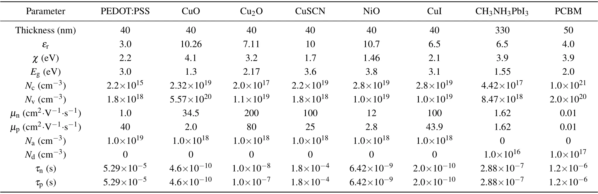
Table 1. Simulation parameters of inverted p-i-n PSCs and ETM-free PSCs.[12-28]
3. Results and discussion
3.1. Simulated performance of ETM-free PSCs and inverted p–i–n PSCs
To investigate the difference between inverted p-i-n PSCs and ETM-free PSCs, four types of PSCs with different structures are studied,i.e., PEDOT:PSS-CH3NH3PbI3-PCBM,CuSCN-CH3NH3PbI3-PCBM,PEDOT:PSSCH3NH3PbI3, and CuSCN-CH3NH3PbI3. I-CH3NH3PbI3with a doping concentration of 1.0×1013cm-3acting as an absorber and PCBM serving as ETM in these p-i-n PSCs.Based on the inverted p-i-n PSC, the ETM-free PSC is designed when PCBM layer is removed and n-CH3NH3PbI3is self-doped by donors with a concentration of 1.0×1016cm-3.
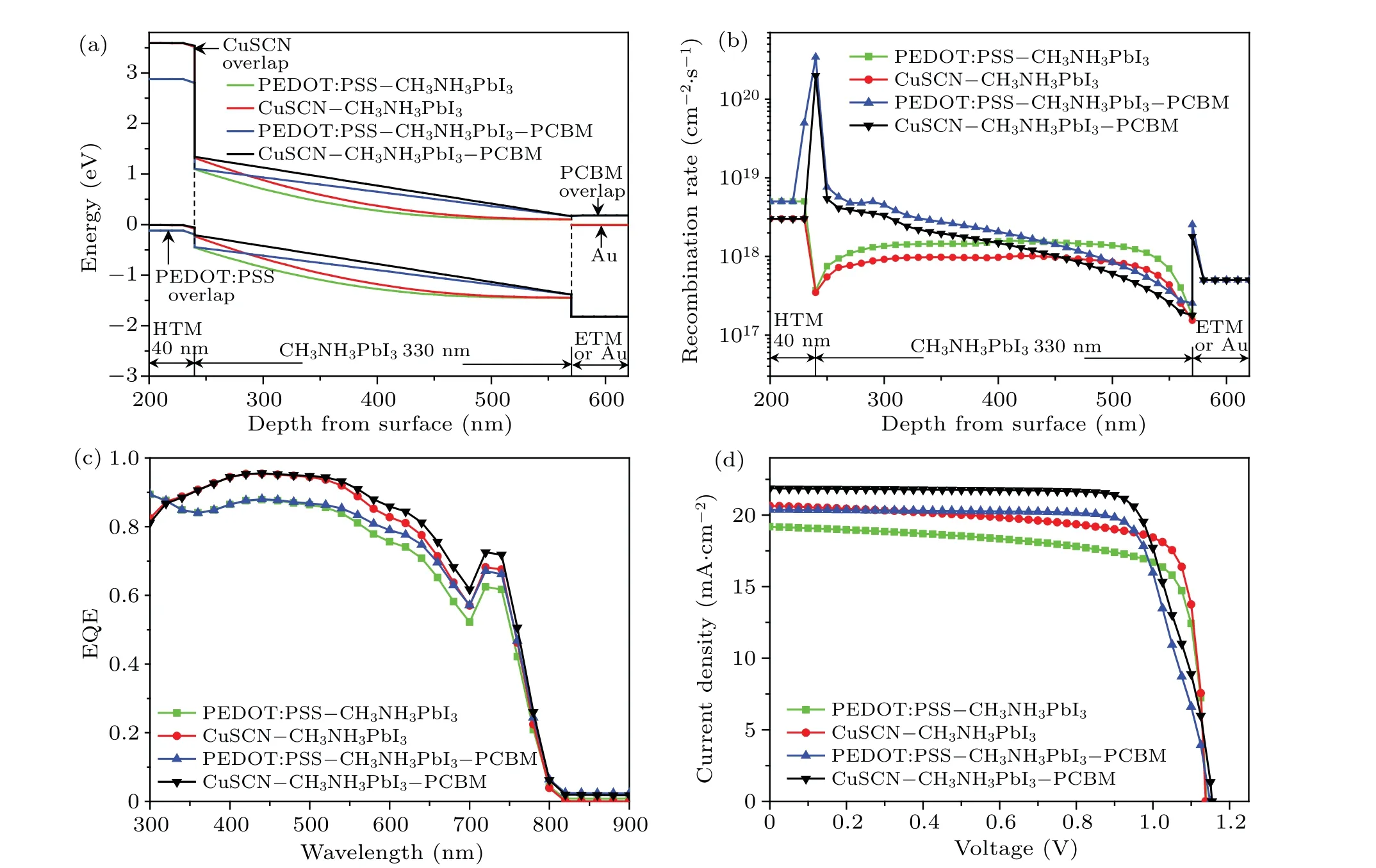
Fig.2. Comparison of performance between ETM-free PSCs and p-i-n PSCs: (a)energy band,(b)recombination rate,(c)EQE,and(d)J-V characteristics.
The energy bands of the four PSCs are illustrated in Fig. 2(a). When p-i-n PSCs are simplified into ETM-free PSCs, bending trend of energy band of CH3NH3PbI3is converted from“linear gradient”type into“abruptly curved”type,which is beneficial for impeding both photogenerated electrons from diffusing into anode and photogenerated holes from diffusing into cathode,leading the reverse saturation current to decrease.Simultaneously,the bending quantities of the energy band of CH3NH3PbI3for p-i-n PSCs and ETM-free PSCs are equal, which means that the total built-in potential difference(VD)is equal. However,comparing with p-i-n PSCs,theVDat 240 nm-450 nm depth of CH3NH3PbI3in ETM-free PSCs is big. As a result,recombination rate in CH3NH3PbI3of ETMfree PSCs is obviously smaller than that of p-i-n PSCs as shown in Fig. 2(b), so that more electron-hole pairs will be separated and collected in ETM-free PSCs.
The external quantum efficiency (EQE) of PSCs is illustrated in Fig. 2(c). Comparing with p-i-n PSC, the EQE of ETM-free PSC slightly decreases in a wavelength range of 450 nm-750 nm. Simultaneously, the EQE of CuSCN is higher than that of PEDOT:PSS in a wavelength range of 330 nm-750 nm, because the electron mobility of inorganic CuSCN (100 cm2·V-1·s-1) is much higher than that of organic PEDOT:PSS(1 cm2·V-1·s-1). TheJ-Vcharacteristics of four PSCs are shown in Fig.2(d). If the graph enveloped byJ-Vcurve and coordinate axis is more matched to rectangle,the fill factor(FF)of the PSC is higher.[5]Obviously,theFFof ETM-free PSC is better than that of p-i-n PSC due to the fact that the graph enveloped by coordinate axis and theJ-Vcurve of the former is closer to a rectangle than that of the latter. In ETM-free PSC, the n-CH3NH3PbI3is heavily doped,the conductivity of material is improved and series resistance(Rs)is reduced,resulting in the compensatedFF.
Simulated performances of four PSCs are listed in Table 2. Obviously,the simulation results are closely coincided with experimental results of p-i-n PSCs, which confirms the reliability of the physical model. Meanwhile,the efficiency of CuSCN-CH3NH3PbI3PSC is 18.56%, which is higher than that of PEDOT:PSS-CH3NH3PbI3-PCBM PSC(18.06%),but lower than that of CuSCN-CH3NH3PbI3-PCBM (19.56%).Obviously,the efficiency of ETM-free PSC decreases down to less than 1.29%by simplifying p-i-n structure,which means that the high efficiency can be achieved by ETM-free PSC with simplified preparation process.
The detailed electric field distribution is shown in Fig.3.Comparing with p-i-n PSC, the electric field intensity in ETM-free PSC is strong in a depth range of 240 nm-450 nm but weak in a depth range of 450 nm-570 nm.Since the generation rate of carriers in absorber decreases exponentially with the increase of thickness, the electron-hole pairs are concentrated mainly on the front surface of CH3NH3PbI3.As a result,the velocity of the carriers in ETM-free PSCs is faster than that in the p-i-n PSCs, thus the electron-hole pairs will be separated faster and the recombination losses of the carriers will be less.
Photogenerated carriers will increase if thickness of CH3NH3PbI3increases,but the effects on ETM-free PSCs and p-i-n PSCs are quite different. It is obvious that the values ofJscof four PSCs increase with a similar tendency whileVoc,FF, and PCE change are quite different when thickness of CH3NH3PbI3increases as illustrated in Figs.4(a)-4(d).
When the thickness of i-CH3NH3PbI3in p-i-n PSC increases, the electric field in CH3NH3PbI3layer remains uniform and gradually decreases, but the distance of carriers transport to electrode increases, leading the bulk recombination losses to increase andVocto decrease. Meanwhile, the series resistance of p-i-n PSC increases rapidly due to low conductivity of i-CH3NH3PbI3andFFdecreasing. The PCE of p-i-n PSCs increases at first because theJscincreases,and then the PCE decrease subtly becauseVocandFFdecrease.
In ETM-free PSCs, heavily doped n-CH3NH3PbI3gives rise to good conductivity and electronic transport capability.Meanwhile, the electric field in n-CH3NH3PbI3keeps unchanged as the thickness of CH3NH3PbI3increases, so recombination losses caused by multiple defects are almost unchanged but photogenerated carriers are increased obviously,soVoc,Jsc,theFFand PCE of ETM-free PSCs keep increasing. Moreover, the PCE of ETM-free PSCs will exceed that of p-i-n type PSC when the thickness of CH3NH3PbI3is over 800 nm, which indicates that the ETM-free PSC can achieve higher PCE when the CH3NH3PbI3layer is thicker.
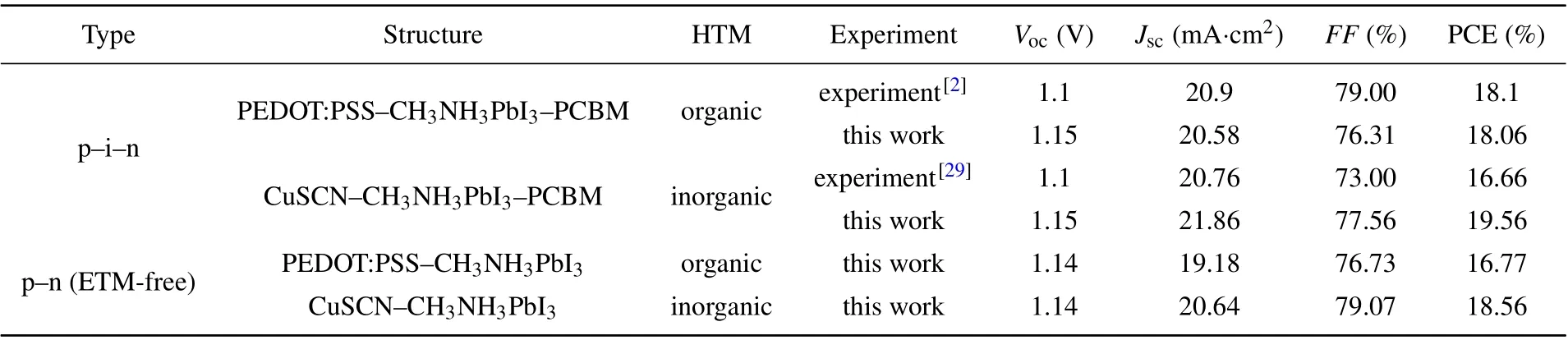
Table 2. Comparison of performance between ETM-free PSCs and p-i-n PSCs.
According to Figs.4(a)-4(d),CuSCN-CH3NH3PbI3PSC shows good performance in comparison with other configurations. The PCE of CuSCN-CH3NH3PbI3PSC is almost saturated when CH3NH3PbI3thickness is larger than 1000 nm. Therefore, 1000 nm is the most suitable thickness for CH3NH3PbI3. Comparing with the famous organic PEDOT:PSS, the performance of CuSCN-CH3NH3PbI3is obviously better than that of PEDOT:PSS-CH3NH3PbI3,which means that efficiency can be improved if CH3NH3PbI3directly contacts the inorganic HTM.

Fig.3. Electric field distributions of different structures: (a)PEDOT:PSS-CH3NH3PbI3-PCBM;(b)CuSCN-CH3NH3PbI3-PCBM;(c)PEDOT:PSSCH3NH3PbI3;(d)CuSCN-CH3NH3PbI3.
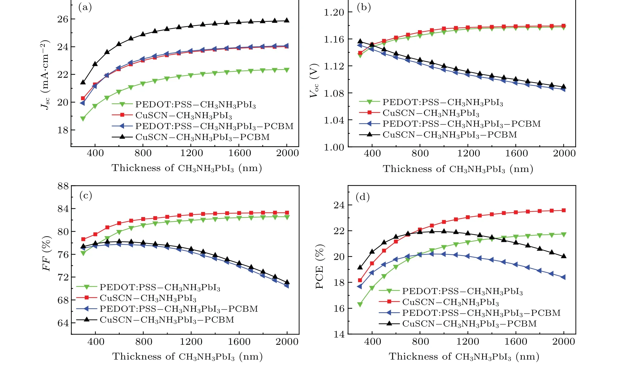
Fig.4. Influences of CH3NH3PbI3 thickness on performances of ETM-free PSC and p-i-n PSC:thickness-dependent: (a)Jsc,(b)Voc,(c)FF,and(d)PCE.
3.2. Comparative study of CuSCN–CH3NH3PbI3 and some typical ETM-free PSCs
In order to study the ETM-free PSCs in depth, five types of ETM-free PSCs are designed by a 330-nm-thick n-CH3NH3PbI3directly combined with different inorganic HTMs,i.e., CuO, Cu2O, CuI, NiO, and CuSCN. To study the influence of band structure on PSC performance, CuO and Cu2O are selected to compare with the wide band gap materials, such as CuSCN, NiO, and CuI. The energy bands of five ETM-free PSCs are illustrated in Fig. 5(a). That the energy band barrier of CH3NH3PbI3in a space charge region is steeper means higher potential difference and stronger built-in electric field.[20]That the electronic barrier at HTMCH3NH3PbI3interface is higher means smaller reverse saturation current from absorption layer to anode.[19]The values of ΔEcof NiO-CH3NH3PbI3and CuSCN-CH3NH3PbI3interfaces are the largest,thus reverse saturation currents of the two PSCs are the smallest.
TheJ-Vcharacteristics of PSCs are shown in Fig. 5(b).Obviously,VocandJscof CuO-CH3NH3PbI3is the smallest among the five PSCs. Because the band gap of CuO is 1.3 eV and the lowest electronic barrier is constructed on CuO-CH3NH3PbI3interface, which causes serious parasitic absorption(Fig.5(c))and large reverse saturation current.The CuI, NiO, and CuSCN show significant improvement inJ-Vcurve,for these materials exhibit higherEgand higher barrier at HTM-CH3NH3PbI3interface. Moreover, the bestFFis obtained by CuSCN-CH3NH3PbI3. TheFFis determined by the energy level matching and series/parallel resistance.[30]An energy barrier of 0.15 eV between the highest occupied molecular orbitals (HOMOs) of CuSCN and perovskite is smaller than that of CuI and NiO,thus parasitic resistance is smaller.
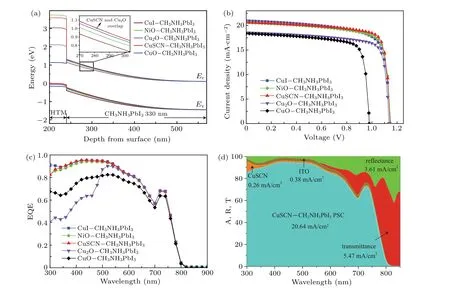
Fig.5. Comparison of performance among ETM-free PSCs,showing(a)energy band versus depth,(b)J-V characteristics,(c)EQE versus wavelength,(d)absorbance(A),reflectance(R),and transmittance(T)versus wavelength of CuSCN-CH3NH3PbI3 PSC.
Table 3 provides the simulation results of ETM-free PSCs. The PCE of CuI-CH3NH3PbI3, NiO-CH3NH3PbI3,CuSCN-CH3NH3PbI3, Cu2O-CH3NH3PbI3, and CuOCH3NH3PbI3PSC is 17.70%,18.04%,18.56%,16.48%,and 13.88%, respectively. Comparatively, CuSCN-CH3NH3PbI3possesses the best structure and its PCE is achieved to be 18.56%. The EQEs of five ETM-free PSCs are shown in Fig.5(c). The EQE of CuSCN-CH3NH3PbI3is the highest in a wavelength range of 350-450 nm.
Figure 5(d) shows the absorbance (A), reflectance (R),and transmittance(T)of CuSCN-CH3NH3PBI3PSC in detail.Reflection loss caused by material refractive index mismatch is 3.61 mA/cm2;transmission loss caused by insufficient absorption is 5.47 mA/cm2. Moreover,the absorption loss caused by the parasitic absorption of CuSCN is 0.26 mA/cm2.
As shown in Tables 2 and 3 and Fig. 5, comparing with organic PEDOT:PSS and other four typical inorganic HTMs,i.e.CuO, Cu2O, CuI, and NiO, the high performance ETMfree PSC can be achieved if HTM is selected as CuSCN.
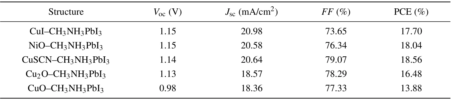
Table 3. Simulated performances of five ETM-free PSCs with different inorganic HTMs.
3.3. Work function of back electrode on performance of CuSCN–CH333NH333PbI333 PSC
The work function of back electrode plays an important role on built-in electric field of PSC and recombination rate of carrier. Work functions of some typical electrode materials,i.e.FTO, Ag, Ti, AZO, ITO, and Au are-4.0 eV,-4.26 eV,-4.33 eV,-4.4 eV,-4.8 eV,and-5.1 eV,respectively.To select an optimal back electrode,the influence of the back electrode work function on CuSCN-CH3NH3PbI3PSC performance is studied. The energy bands of the CuSCNCH3NH3PbI3are shown in Fig. 6 with different back electrodes. The energy band of CH3NH3PbI3gradually sinks down and the Schottky barrier between CH3NH3PbI3and the back electrode decreases gradually with the increase of the back electrode work function, which reduces the electron backflow to the electrode and the accumulation of photogenerated electrons in the barrier region. Therefore,the recombination rate of electron-hole pairs decreases. When the material of the back electrode is FTO,the height of the Schottky barrier on the back surface of CH3NH3PbI3is equal to 0. At the moment,CH3NH3PbI3and FTO form a good energy band match.Therefore,in order to achieve a good charge transfer,the FTO is a suitable back electrode material.
Figure 7(a) shows the influence of the back electrode work function on the performance of CuSCN-CH3NH3PBI3PSC.The PCE increases linearly with the back electrode work function increasing from-5.2 eV to-4.0 eV.Once the work function exceeds-4.0 eV, the PCE of the PSC tends to be saturated. Therefore, in order to achieve a good PCE value,the back electrode work function of CuSCN-CH3NH3PBI3PSC should not be less than-4.0 eV. In addition, when the work function of back electrode is-4.0 eV, theJ-Vcharacteristic curve of CuSCN-CH3NH3PbI3PSC is overlapped with Ohmic contact curve as shown in Fig.7(b).
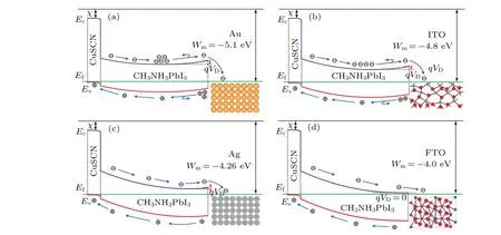
Fig.6. Energy bands of CuSCN-CH3NH3PbI3 with different electrode materials: (a)Au,(b)ITO,(c)Ag,(d)FTO.

Fig.7. (a)Device performance of CuSCN-CH3NH3PbI3 versus work function of back electrode,and(b)J-V curves.
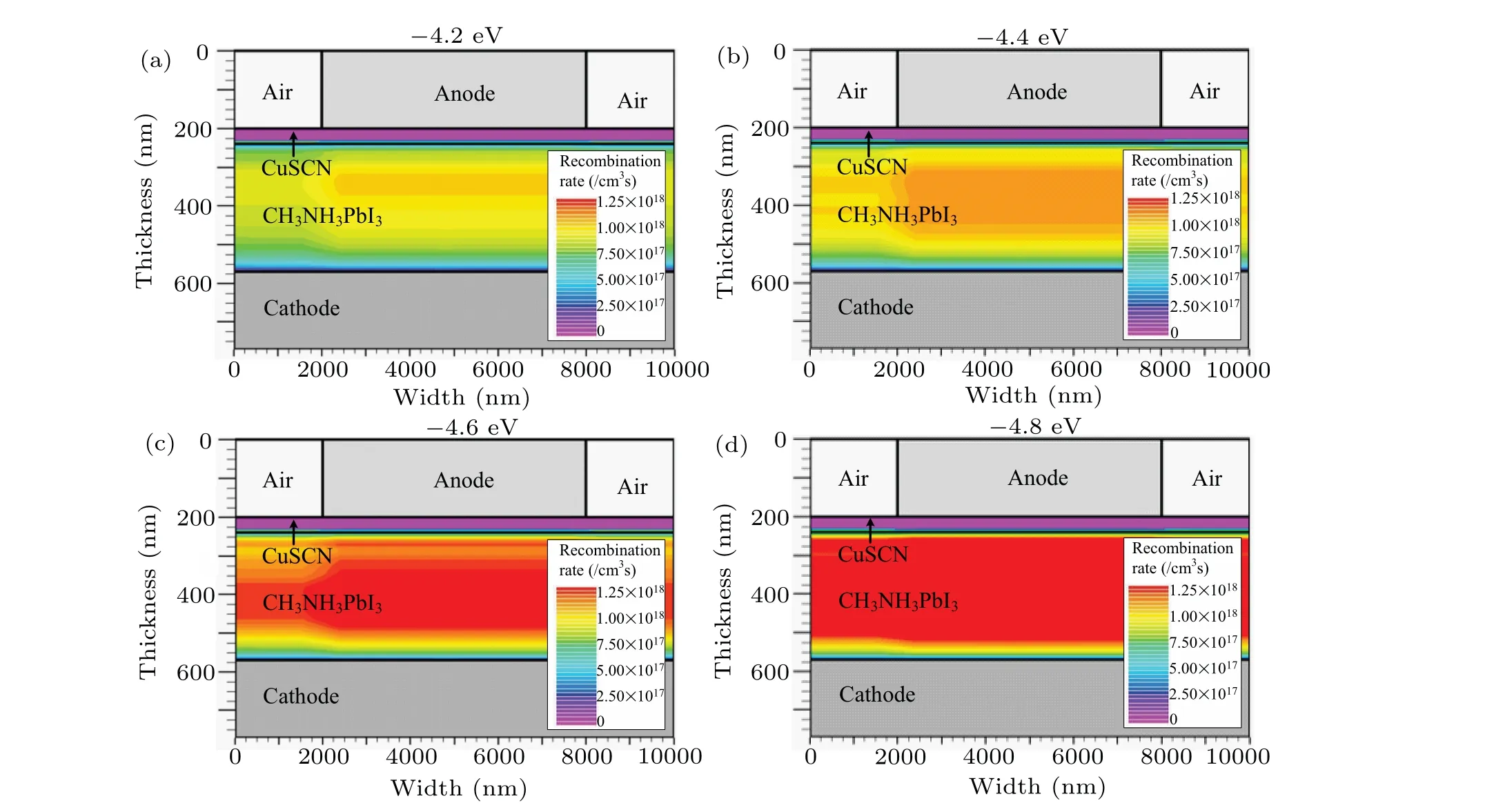
Fig.8. Recombination rate distributions in CuSCN-CH3NH3PbI3 PSC with different work functions of back electrode: (a)-4.2 eV,(b)-4.4 eV,(c)-4.6 eV,and(d)-4.8 eV.
Recombination loss occurs mainly in bulk of CH3NH3PbI3because of the energy band bending. Figure 8 shows that the recombination rate of carrier increases rapidly from 5.0×1017cm-3/s to 1.25×1018cm-3/s when the work junction of back electrode decreases from-4.2 eV to-4.8 eV.In view of this, the FTO with a work function of-4.0 eV is selected as an appropriate back electrode material.
3.4. Influence of band gap of CH333NH333PbI333 on performance of CuSCN–CH333NH333PbI333 PSC
The research shows that the band gap of perovskite(ABX3) can be tuned in a range of 1.17 eV-4.09 eV by controlling the atomic ratio of Cs/FA/MA, Pb/Sn or I/Br/Cl.[30]Simultaneously, the gradient band gap perovskite can be fabricated by the ion exchange and spin coating method.[31,32]In this subsection,the effect of CH3NH3PbI3band gap on ETMfree PSC performance is investigated based on the former optimized HTM CuSCN,back electrode and CH3NH3PbI3thickness. The band gap distribution of CH3NH3PbI3has three structures according to the law of linear change,i.e.uniform structure, gradient decreasing structure, and gradient increasing structure(see Fig.9).
Obviously,the photogenerated holes of gradient decreasing structure need to overcome an energy band barrier in the transport process, resulting in a large number of photogenerated holes remaining in the absorption layer andJscdecreasing. Compared with uniform structure band gap and gradient decreasing structure band gap, the gradient increasing band gap can form a good valence band energy level that promotes hole transport and reduces carrier recombination loss.
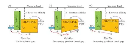
Fig. 9. Schematic diagram of CuSCN-CH3NH3PbI3 PSC with different band gaps of CH3NH3PbI3: (a) uniform structure, (b) gradient decreasing structure,and(c)gradient increasing structure.
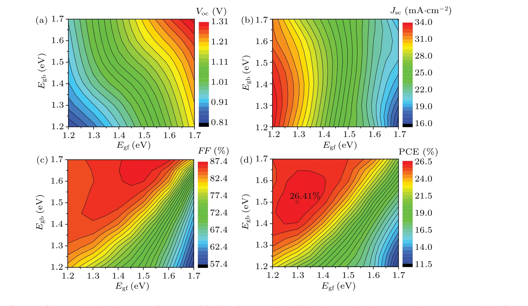
Fig.10. Influences of CH3NH3PbI3 band gap on performances of CuSCN-CH3NH3PbI3 PSC,showing Egf-dependent(a)Voc,(b)Jsc,(c)FF,and(d)PCE.
TheVoc,Jsc,FF, and PCE of ITO-CuSCNCH3NH3PbI3-FTO PSCs varying with band gap of CH3NH3PbI3are depicted in Figs. 10(a)-10(b). TheEgfandEgbrepresent the band gap of the front surface and back surface of CH3NH3PbI3, respectively. TheVocincreases significantly with the increase ofEgforEgb. However,the effect ofEgfis stronger than that ofEgb. Because the PSC is irradiated from the front side, the number of the generated carriers is higher. Therefore,more carriers to separate at the front interface result in higher influence ofEgf. This also explains that theEgfhas a greater influence on theJsc. TheFFreaches a maximum value whenEgfis 1.4-1.5 eV andEgbis 1.6-1.7 eV,which is because the difference in conduction band between the CuSCN interface and the CH3NH3PbI3interface is close to 0, resulting in the smallest parasitic resistance. Simultaneously,the gradient increasing structure forms whenEgb>Egf,which accelerates hole drift and reduces the recombination rate. Finally, the PCE reaches a maximum value of 26.41%whenEgf= 1.3 eV andEgb= 1.5 eV. Comparing with the uniform band gap of 1.55 eV,the optimization of the gradient band gap increases the PCE by 3.74%(see Table 4).
3.5. Influences of doping and defect of CH333NH333PbI333 on property of CuSCN–CH333NH333PbI333 PSC
Conductivity of material and built-in electric field of heterojunction are determined mainly by doping concentration of CH3NH3PbI3and HTM in ETM-free PSCs.In this subsection,the device performance of ITO-CuSCN-CH3NH3PbI3-FTO PSC varying with donor concentration(Nd)of CH3NH3PbI3is discussed based on the former optimized CH3NH3PbI3thickness and band gap(see Fig.11(a)). TheVocincreases linearly withNdof CH3NH3PbI3increasing from 1.0×1015cm-3to 1.0×1018cm-3due to the fact that the fermi level of CH3NH3PbI3is closer to the conduction band minimum and the built-in electric field increases. TheJscdecreases significantly whenNdof CH3NH3PbI3exceeds 1.0×1016cm-3,which results from the width of space charge region decreasing, separation of electron-hole pair decreasing, and radiative recombination increasing. Optimal doping will increase conductivity and improve theFF. Finally, the PCE achieves a maximum value of 26.64% whenNdof CH3NH3PbI3is 5.0×1016cm-3.
The performance versus bulk defect density (Nt) of CH3NH3PbI3is presented. There are four types of bulk defects in material usually,i.e.,Gaussian acceptor defects,Gaussian donor defects,conductor-tail defects,and valence-tail defects. In this work, the influence of Gaussian acceptor defects in CH3NH3PbI3on PSC performance is studied (see Fig. 11(b)). TheVoc,Jsc,FF, and PCE of the PSC drop significantly whenNtexceeds 1.0×1015cm-3. Owing to the fact that the recombination rate increases withNtincreasing, and the concentration of majority carriers decreases, both builtin voltage of heterojunction and conductivity of material decrease. In order to achieve high efficiency, the bulk defect density in CH3NH3PbI3should be controlled to be less than 1.0×1015cm-3.
The influence of CuSCN thickness on the performance of CuSCN-CH3NH3PbI3PSC is shown in Fig. 11(c). The distance between photogenerated hole and electrode increases with the CuSCN thickness increasing, so the recombination rate and the bulk resistance increase,which leads theJsc,FF,Voc, and PCE of the PSC to decrease linearly. As a result,the PCE of the PSC decreases by 0.3%when the thickness of CuSCN increases from 10 nm to 1000 nm. If the thickness of CuSCN decreases,the PCE of CuSCN-CH3NH3PbI3PSC will be improved.
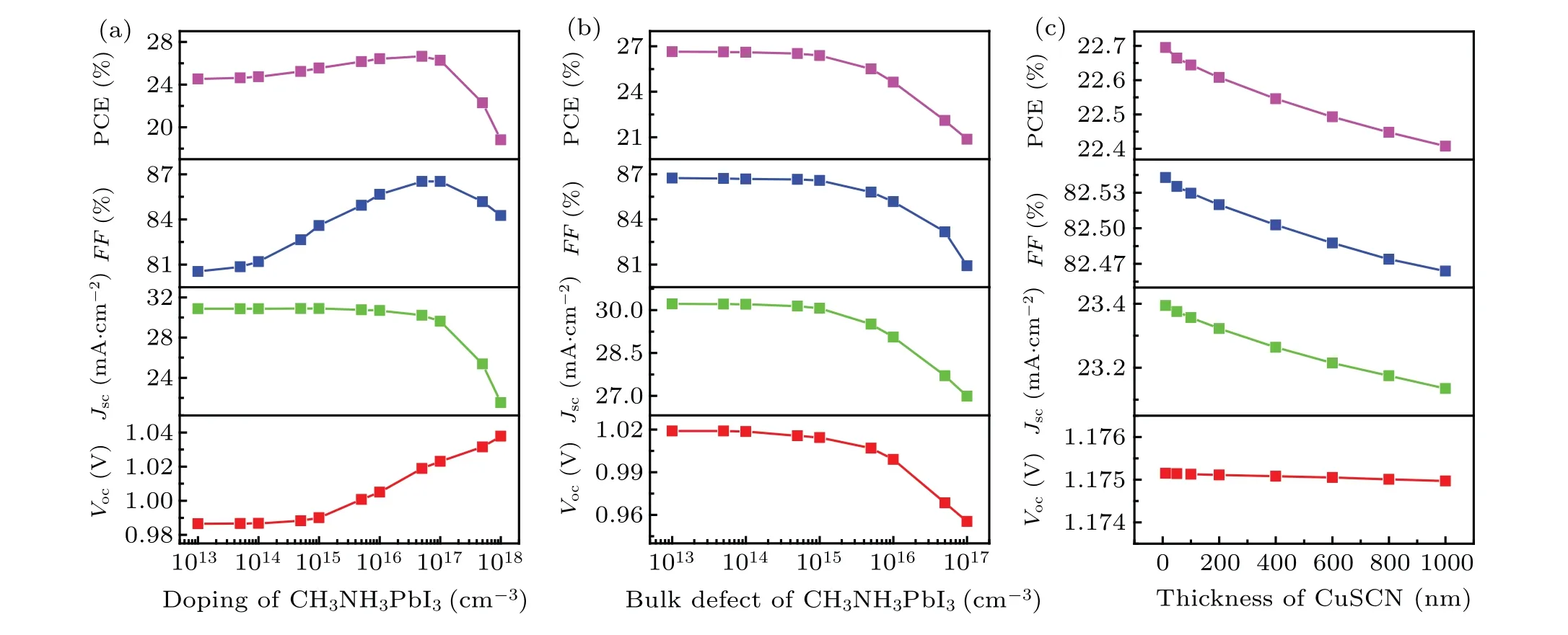
Fig.11. Variations of CuSCN-CH3NH3PbI3 cell performance with(a)doping of CH3NH3PbI3,(b)bulk defect of CH3NH3PbI3,and(c)thickness of CuSCN.
3.6. Influences of light and temperature on property of CuSCN–CH333NH333PbI333 PSC
Figures 12(a) and 12(b) show that the electron current density and hole current density of the CuSCN-CH3NH3PBI3PSC significantly decrease under the solar irradiance from the vacuum environment (AM0) to the earth’s surface (AM1.5),which leads to a smallerJ-Vcharacteristic and a 2.83% reduction in PCE.
As shown in Figs.12(c)-12(d), theVocand PCE of PSC gradually decrease while the current density does not change significantly with the increase of temperature. Because the increase of temperature will cause the stress and strain to increase, which will lead the absorption layer the absorption layer to be distorted and disordered. Therefore,both the radiative recombination and the surface recombination of electronhole pairs increase. Obviously, better photoelectric performance can be obtained in low temperature environment.
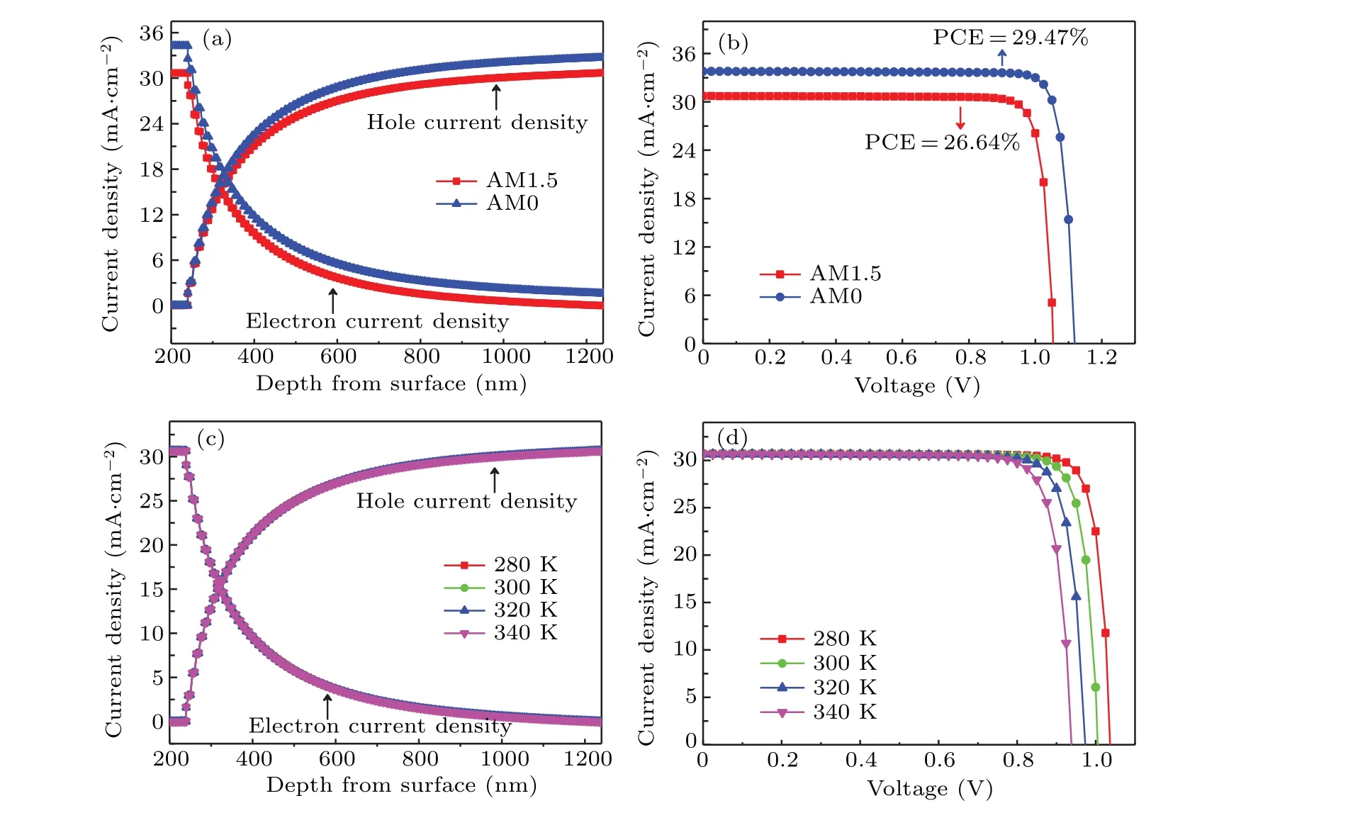
Fig.12. Influences of light on performances of CuSCN-CH3NH3PbI3 PSC:(a)current density and(b)J-V characteristics. Influences of temperature on performance CuSCN-CH3NH3PbI3 PSC:(c)current density and(d)J-V characteristics.
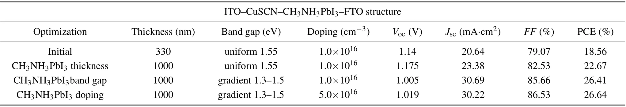
Table 4. Performances of ITO-CuSCN-CH3NH3PbI3-FTO during optimization.
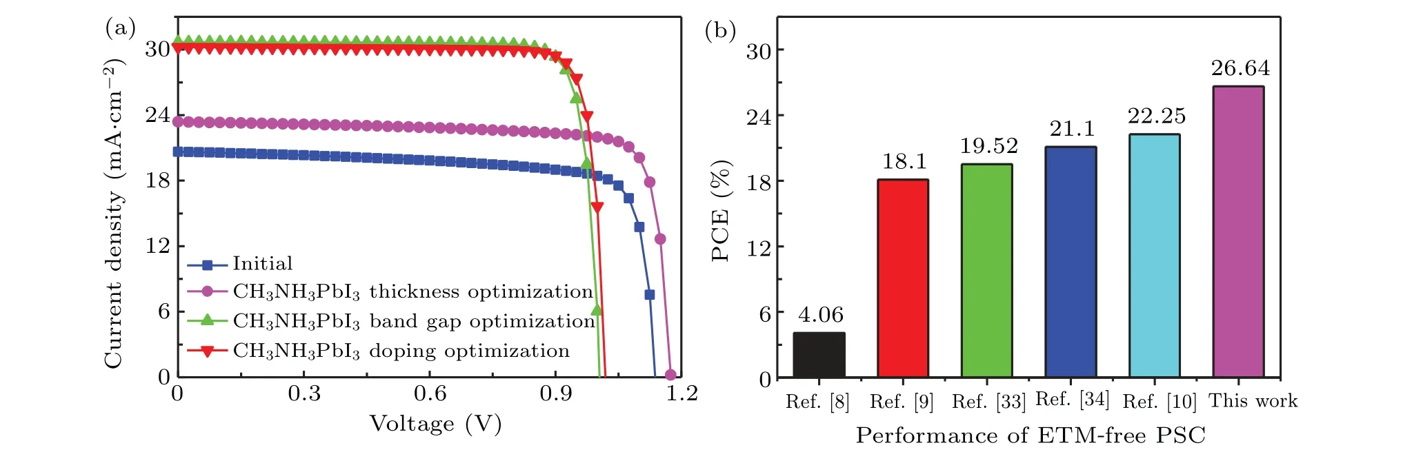
Fig.13. (a)The J-V characteristics of ITO-CuSCN-CH3NH3PbI3-FTO during optimization,(b)comparison among performances of ETM-free PSC cited from some reports.
In this paper,the structural advantages,material selection and some physical parameters of ETM-free PSC are studied in detail, and the PCE increases from 18.6% to 26.64% (see Table 4 and Fig. 13). However, there are still many aspects worth further studying. The first item is doping distribution types of the perovskite layer,i.e., gradient type, exponential type or Gaussian type;the second item is the mobility of perovskite,which can be adjusted by changing the ratio of Sn/Pb atoms;[30]the third item is the designing of a double HTM to enhance the extraction velocity of photo-generated holes; the last item is the transparent conductive oxide FTO as the back electrode, which can further use diffuse reflected light to enhance cell efficiency.[35]These studies can provide a certain reference for the future researches.
4. Conclusions
Focused on CuSCN-CH3NH3PbI3,a series of planar heterojunction PSCs with ETM-free structure and p-i-n structure are compared and numerically analyzed by the TCAD Atlas. Compared with PEDOT:PSS, Cu2O, CuI, CuO, and NiO, the CuSCN is an excellent inorganic HTM for building ETM-free PSCs due to its high charge mobility, good energy band structure,and high EQE.Moreover,owing to the unique electric field structure, high conductivity and incident sunlight absorption, the performance of CuSCN-CH3NH3PbI3ETM-free PSC is better than those of p-i-n PSCs. Simultaneously, the gradient increasing band gap of CH3NH3PbI3can improve significantly the hole transport and increaseJscandFF. Furthermore, the influences of the thickness, doping, and defect of CH3NH3PbI3on performance of CuSCNCH3NH3PbI3PSC are analyzed in detail. The efficiency of ETM-free can be improved to 26.64% by CuSCN and gradient increasing CH3NH3PbI3. Importantly, gradient band gap perovskite can be fabricated by ion exchange or spin coating technology,which is simple and low cost. This study provides a guide for designing and fabricating the ETM-free PSCs.
Acknowledgements
Project supported by the Fundamental Research Funds for the Central Universities of China (Grant No.JD2020JGPY0010)and the China Post-Doctoral Science Foundation(Grant No.2020M671834).
猜你喜欢
杂志排行

Chinese Physics B的其它文章
- Superconductivity in octagraphene
- Soliton molecules and asymmetric solitons of the extended Lax equation via velocity resonance
- Theoretical study of(e,2e)triple differential cross sections of pyrimidine and tetrahydrofurfuryl alcohol molecules using multi-center distorted-wave method
- Protection of entanglement between two V-atoms in a multi-cavity coupling system
- Semi-quantum private comparison protocol of size relation with d-dimensional GHZ states
- Probing the magnetization switching with in-plane magnetic anisotropy through field-modified magnetoresistance measurement