Defect calculations with quasiparticle correction:A revisited study of iodine defects in CH3NH3PbI3
2022-01-23LingLi李玲andWanJianYin尹万健
Ling Li(李玲) and Wan-Jian Yin(尹万健)
1College of Energy,Soochow Institute for Energy and Materials Innovations(SIEMIS),and Jiangsu Provincial Key Laboratory for Advanced Carbon Materials and Wearable Energy Technologies,Soochow University,Suzhou 215006,China
2Light Industry Institute of Electrochemical Power Sources,Soochow University,Suzhou 215006,China
3Key Laboratory of Advanced Optical Manufacturing Technologies of Jiangsu Province&Key Laboratory of Modern Optical Technologies of the Education Ministry of China,Soochow University,Suzhou 215006,China
Keywords: quasiparticle correction,defect calculation,GW theory,methylammonium lead iodide
1. Introduction
As crucial features in functional semiconductors, defect properties, typically as defect formation and transition energies,are generally calculated using the first-principle densityfunctional theory (DFT) based on different approximations of exchange-correlation functionals such as local density approximation (LDA), grand gradient approximation (GGA),and hybrid functionals.[1-10]DFT based on LDA/GGA is known to be reliable for calculating the total energies of a bulk system that is free of defect states.[11-14]However,owing to the existence of artificial self-interaction and the absence of the derivative discontinuity in the exchange-correlation potential,DFT-LDA/GGA does not accurately estimate the electronic eigenvalues,resulting in the underestimation of the band gap and inaccurate positioning of the single-electron defect level.[2,15-18]Although the hybrid functional method can reproduce the experimental band gap,it is,to some extent,still an empirical approach,as the exact exchange portion is an empirical parameter.[2,19,20]In addition,its reliability in calculating the position of defect states has been challenged.[2,5,19,21]The GW approach,based on the many-body perturbation theory applied to Green’s function,provides a more rigorous theoretical framework for the improvement of the estimation accuracy of a band gap and single-electron level.[22,23]However,owing to the heavy computational cost,the total energy calculations,and thus atomic relaxations,have not been effectively implemented within the framework of the GW method.[24,25]
In this work,we combined the total energy calculation at the DFT level with the single-electron level calculation of the GW method to improve the accuracy of defect calculations.As a case study, we applied this approach to investigate iodine vacancies and iodine interstitials in CH3NH3PbI3,a class of prevalent defects existing in an emerging perovskites solar cell, which are believed to be responsible for the nonradiative recombination of photoexcited carriers.[26]Recent DFT calculations have yielded scattered results for the transition levels of VIand Ii,[9,27-31]as shown in Fig. 1. For example,VIwas initially considered to introduce shallow defect levels,with a transition level at the conduction band minimum of(CBM)+0.01 eV.[9]In contrast to conventional models where VIis a donor, in this study, VIwas able to acquire an additional electron,attained a stable dimer structure,and obtained a deep transition level below the CBM.[30]
Defect calculations via PBE,PBE-SOC,and hybrid functional plus spin-orbit coupling (HSE-SOC) have also been performed for comparison with GW-SOC approaches. It has been found that GW-SOC generally pulls down the singleelectron level for the occupied state and pushes up the singleelectron level for the unoccupied state. The GW-SOC approach predicted neutral Iito be unstable and that the transition level of Ii(+1/-1) is close to the valence band maximum(VBM),therefore,the level of Iimay not be as detrimental as previously reported. GW-SOC calculations additionally showed that VImay be unstable in the-1 charged state, in contrast to previous reports,but could still be detrimental due to the deep transition level of VI(+1/0). GW results are consistent with the experiment reporting a shallow donor level close to the CBM.[32]These results help further understand the intrinsic point defect and defect passivation observed in CH3NH3PbI3.
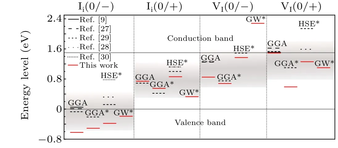
Fig.1. Transition levels of VI and Ii were reported in the literatures and this work.For ease of comparison,we unified the band gap to 1.5 eV.The red line represents the data of this work. The star*indicates that the SOC effect was considered. The rendering band represents the approximate position range of the iodine defect charge transition energy level in the band gap obtained by combining all the current data work.
2. Calculation methods
We performed first-principles calculations based on the density functional theory (DFT) implemented in the VASP program. The electron-ion interactions were described by projector augmented wave(PAW)potentials. The generalized gradient approximation (GGA) of PBE, HSE, and the quasiparticle GW method was used as exchange-correlation functionals.β-CH3NH3PbI3was used to study the native iodine defect. The PBE method was used to optimize the lattice constants(a=8.69 ˚A andc=12.66 ˚A)of the bulk structure. The 2×2×1 supercell structure and the subsequent defect structure were constructed based on this structure. The valence wave function was extended based on the plane wave sets with an energy cutoff of 300 eV. All atoms were relaxed to minimize the Hellmann-Feynman force to less than 0.01 eV /˚A.An identical convergence standard was used at all calculation levels. OnlyΓpoint was considered as the k-point sampling in the Brillouin zone in defect calculation.
3. Results and discussion
3.1. GW-correction on single-electron levels
Defect calculations based on first-principles calculations are often performed on a mixed scheme to combine the advantage of the specialk-point andΓpoint-only approaches.[23]The formation energy based on DFT-PBE calculations is accordingly given by
where the first two terms are related to total energies and the third term is concerning the single-electron energy level. In our approach,the total energy term and single-electron energy level were calculated with the PBE and GW-SOC approaches,respectively.
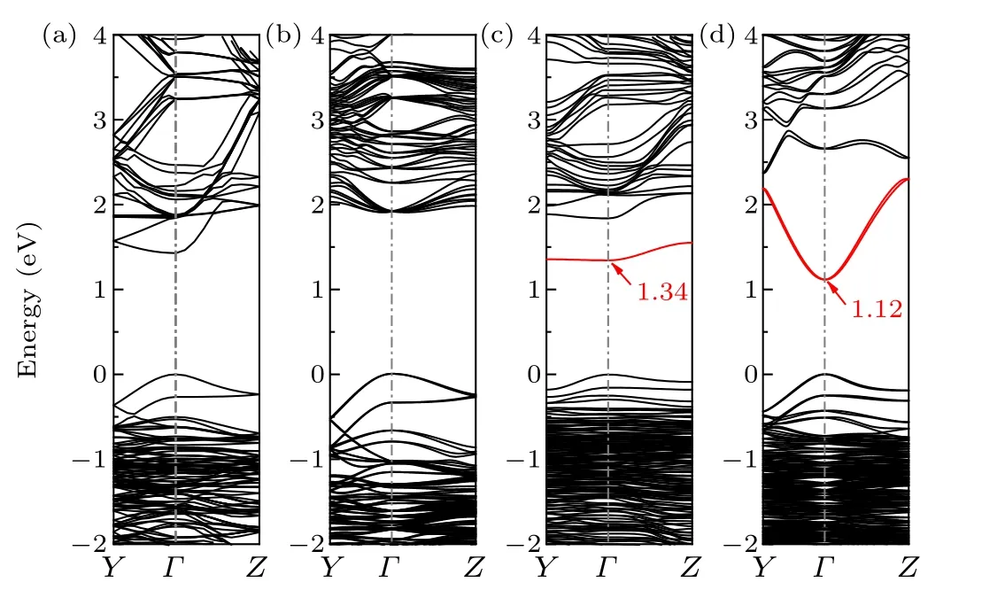
Fig. 2. Band structure of bulk CH3NH3PbI3 obtained through the (a)PBE calculation and (b) GW-SOC calculation. Band structure of defective CH3NH3PbI3 with V1I (dimer structure)obtained through the(c)PBE calculation and(d)GW-SOC calculation. The red lines indicate the defect band.

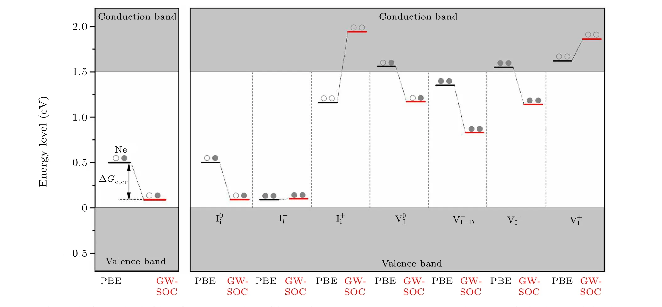
Fig.3. Single-electron level of defective CH3NH3PbI3 at different charge states in PBE and GW-SOC calculations. The levels are scaled to the band gap of 1.5 eV.The electronic occupancy is also shown.
3.2. GW-correction on defect calculations
Using the GW method, we recalculatedετD(0)-εVBM(host)for iodine defects with different charge states and compared them with the results under a traditional PBE calculation. The difference in the single-electron level allowed us to introduce a GW correction term for correction of the singleelectron level in the traditional PBE calculation as shown in Eq. (1). Taking the electronic occupancy into consideration,the defect formation energy after GW correction is accordingly obtained by the following formula:
3.3. Multiple defect configurations
In conventional semiconductors such as Si, GaAs, and CdTe, point defects (vacancies, substitution and interstitials)are often formed in a rigid model, where the defect configurations only have little relaxations or distortions away from the original perfect crystal lattice.[35,36]However, in CH3NH3PbI3with a soft lattice, iodine interstitials and vacancies demonstrate multiple defect configurations, complicating defect calculations.[37]Since the local configurations directly determine the electronic and optoelectronic properties of defects, it is necessary to identify the multiple defect configurations of iodine vacancies and interstitials. It has been clarified that CH3NH3PbI3has both obvious ionicity and covalency.[9,30]The defect configurations can be based on a rigid model as in ionic crystals, and Pb-Pb and I-I wrong bonds can be formed as in covalent crystals.
In the conventional picture,the iodine interstitials should be an acceptor thus negatively charged,which is then favorable for bonding with positively charged Pb cations, as shown in Fig.4(b),forming a bridge configuration where the Pb-I bonds are 3.17 ˚A and 3.25 ˚A, respectively. Those bond lengths are close to the Pb-I bond length in crystal CH3NH3PbI3. Therefore,the bridge configuration is akin to the ionic picture,where the negatively charged I anions bond to the positively charged Pb cations. It was also found that the iodine interstitial can be positively charged and form the I-I wrong bond as in the I3trimer configuration shown in Fig.4(a).In I3trimer configurations,the middle interstitial iodine forms a short(2.85 ˚A)and a long(3.71 ˚A)bond with neighboring I.In the neutral state,the I3trimer configuration is stable,but the middle I interstitial moves to the center with the short(3.56 ˚A)and long(3.33 ˚A)bond lengths being much closer to each other.
For iodine vacancies, our previous results show that it is a stable configuration,as shown in Fig.4(d),where the iodine atom was taken out of the crystal lattice and the lattice has minimal relaxation. The nearby Pb atoms were 6.42 ˚A away from each other, only slightly larger than the distance in perfect crystals (6.29 ˚A). In the conventional picture, the iodine vacancy should be a donor thus its negatively charged states were not considered in our previous calculations. However,Agiorgousiset al.found that an iodine vacancy can capture one electron and form a Pb-Pb dimer configuration as shown in Fig. 4(c), where two Pb form a Pb-Pb wrong bond with a bond length of 3.35 ˚A, much less than their distance in a perfect crystal lattice. Such dimer configurations, as a reflection of strong covalency,were energetically favorable over the non-dimer structure[Fig.4(d)]by 0.67 eV in the-1 charged state. The dimer configurations are metastable in neutral and+1 charged states. The underlying mechanisms of stability on dimer and non-dimer configurations at different charged states have been discussed in our previous studies and are not extensively discussed here.
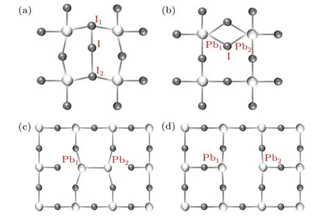
Fig.4.(a)Crystal structure of CH3NH3PbI3and defective CH3NH3PbI3 with(a)the trimer Ii,(b)the bridge Ii,(c)the dimer VI,and(d)non-dimer VI.
In iodine vacancies,when the dimer(non-dimer)configuration is stable in a particular charged state, the non-dimer(dimer)configuration is metastable. There is a kinetic barrier between the stable and metastable stable configurations. Likewise, in I interstitials, when the bridge (trimer) configuration is stable,trimer(bridge)configuration was found unstable.
3.4. Transition energy and formation energy
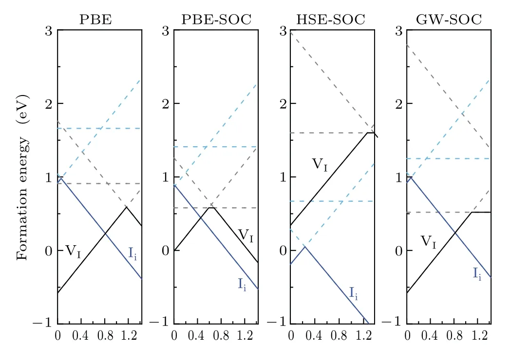
Fig.5. Formation energies of iodine vacancies and interstitials in PBE,PBESOC, HSE-SOC, and GW-SOC calculations. For ease of comparison, we unified the band gap to 1.43 eV.The band gap was calculated by PBE method.
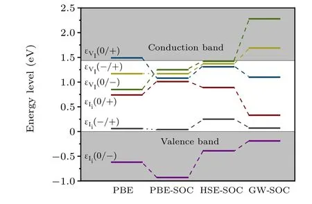
Fig. 6. Transition levels of iodine vacancies and interstitials in PBE, PBESOC,HSE-SOC,and GW-SOC calculations.
4. Conclusion
We developed a GW quasiparticle correction approach for calculating defects and revisited iodine vacancy and interstitial defects in CH3NH3PbI3as a proof of concept. The results were then compared to the results from PBE, PBE-SOC,and HSE-SOC to provide a comprehensive view of iodine defects in CH3NH3PbI3. The results showed that GW-SOC generally pulls down the single-electron level for occupied states and pushes up the single-electron level for unoccupied states.Consistent with previous calculations,GW-SOC predicted that the neutral I interstitial was unstable and the transition level of(+1/-1) was close to the VBM. Therefore, Iimay not be as detrimental as previously reported. Moreover, this study predicted that VImay be unstable in the-1 charged state but could still be detrimental owing to the deep(+1/0)transition level(0.34 eV below CBM).These results based on quasiparticle correction at the single-defect level could further facilitate the understanding of the intrinsic point defect and defect passivation observed in CH3NH3PbI3.
Acknowledgments
Project supported by the National Natural Science Foundation of China (Grant No. 11974257), the Distinguished Young Talent Funding of Jiangsu Province, China (Grant No. BK20200003), the Priority Academic Program Development of Jiangsu Higher Education Institutions (PAPD). DFT calculations were carried out at the National Supercomputer Center in Tianjin[TianHe-1(A)].
猜你喜欢
杂志排行

Chinese Physics B的其它文章
- Superconductivity in octagraphene
- Soliton molecules and asymmetric solitons of the extended Lax equation via velocity resonance
- Theoretical study of(e,2e)triple differential cross sections of pyrimidine and tetrahydrofurfuryl alcohol molecules using multi-center distorted-wave method
- Protection of entanglement between two V-atoms in a multi-cavity coupling system
- Semi-quantum private comparison protocol of size relation with d-dimensional GHZ states
- Probing the magnetization switching with in-plane magnetic anisotropy through field-modified magnetoresistance measurement