Vacuum-gap-based lumped element Josephson parametric amplifier
2022-01-23SishiWu吴思诗DengkeZhang张登科RuiWang王锐YulongLiu刘玉龙
Sishi Wu(吴思诗) Dengke Zhang(张登科) Rui Wang(王锐) Yulong Liu(刘玉龙)
Shuai-Peng Wang(王帅鹏)1, Qichun Liu(刘其春)4, J S Tsai(蔡兆申)2,3, and Tiefu Li(李铁夫)4,5,‡
1Quantum Physics and Quantum Information Division,Beijing Computational Science Research Center,Beijing 100193,China
2Department of Physics,Tokyo University of Science,Kagurazaka,Shinjuku-ku,Tokyo 162-8601,Japan
3RIKEN Center for Quantum Computing(RQC),2-1 Hirosawa,Wako,Saitama 351-0198,Japan
4Beijing Academy of Quantum Information Sciences,Beijing 100193,China
5School of Integrated Circuits,and Frontier Science Center for Quantum Information,Tsinghua University,Beijing 100084,China
Keywords: Josephson parametric amplifier,vacuum gap,quantum-limit noise
1. Introduction
Parametric amplifiers are mostly pumped nonlinear oscillators, among which Josephson parametric amplifier (JPA) is a primary candidate for superconducting circuits.[1-6]Josephson junctions provide not only lossless non-linearity but also the flexibility of working points.In the last decades,Josephson junctions have been employed to realize the quantum-limited parametric amplifier, which plays quite important roles in,e.g., single-shot readout,[7-9]quantum state squeezing,[10,11]and quantum jump trajectory.[12]With the emerging of noisy intermediate-scale superconducting quantum technology (NISQ),[13-15]wide bandwidth amplifiers with quasi quantum-limit noise are quite in demand for fault-tolerant quantum computing.
The mainstream of existing wide bandwidth JPA can be sorted into traveling-wave-based and lumped-element-based types. On the aspect of gain response, traveling wave parametric amplifiers(TWPAs)[16-18]typically provide gain above 10 dB with bandwidth of several-Gigahertz,while lumped element Josephson parametric amplifiers (LJPAs)[19-22]commonly have 100-MHz bandwidth accompanied with gain of 20 dB. On the fabrication aspect, TWPAs need reliable fabrication for series of thousands of Josephson junctions, and LJPAs are composed by superconducting quantum interference device (SQUID) and lumped capacitor, like interdigitated capacitor,[22]and parallel-plate capacitor.[23-25]It is worth noting that,to preserve working region,capacitors with small parasitic inductance,such as parallel-plate capacitor and vacuum-gap-based capacitor, are preferred. While parallelplate capacitor lowers parasitic inductance of the interdigitated capacitor,its multi-layer structure introduces fabrication complexity and amorphous heterogeneous interface, where surface defects are most likely to be found. Although most JPA devices have declared quasi quantum-limit noise, further decreasing defects makes a considerable difference on qubit readout fidelity,which is a key limitation for current scalability of quantum computing.
Typical wideband LJPA design takes comparatively large lumped element capacitance, and skips coupling capacitors to the environment. These lead to wider spectral linewidth, but smaller impedance, due to the limitation of characteristic frequency. To lower impedance mismatch at the signal reflection interface, impedance transformers becomes a common choice, among which, coplanar waveguide (CPW) based one is a primary candidate for its simple designable structure.[26-29]Commonly used CPWbased impedance transformers are composed of a quarterwavelength CPW section (with main characteristic parameters including resonant frequencyωqand impedanceZq) and a half-wavelength CPW section (withωhandZh). According to transmission line theory, input impedance of a load can be transformed via CPW section,which can be expressed asZin(ωs) =Zcpw{ZL+ iZcpwtan(2π¯νωs/ωcpw)}/{Zcpw+iZLtan(2π¯νωs/ωcpw)}. The variables labeled with ‘cpw’refer to parameters of the CPW section,ZLrefers to load impedance,andωsrefers to probe signal frequency.[26]Therefore, forωs≈ωcpw, quarter-wavelength CPW section (with¯ν=1/4)edits the real part of the input impedance,and halfwavelength CPW section (with ¯ν=1/2) balances the imaginary part. Introduction of auxiliary impedance engineering helps break gain-bandwidth product limitation of LJPA to be several-hundred-Megahertz bandwidth accompanied with gain about 20 dB.[23,30,31]
In this paper, we propose an LJPA with vacuum-gapbased capacitor. Aluminum-based microelectronic processing is adopted, which means the design can be integrated for Josephson-junction-based on-chip superconducting quantum computing system. The lumped capacitor using vacuumgap-based structure results in lower parasitic inductance and smaller amorphous heterogeneous interface.[32]The separated superconducting pads are patterned via photo lithography,while the quasi-floating one requires extra evaporation and wet etching. Multi-material fabrication,including amorphous silicon,[21,23,31]silicon nitride,[31]or silicon oxide[30]to form capacitor gaps are avoided. Pad size is designed comparatively larger, in order to certificate structural ductility and process reliability of the vacuum-gap-based capacitor. Additionally, the device is strongly coupled to the environment via a CPW-based impedance transformer to increase gain bandwidth.[26,27]
2. Theory
In the perspective of theoretical analysis, the Josephson junctions embedded circuit can be treated as nonlinear cavity.With external pump,circuit Hamiltonian can be mapped onto a parametric amplifier.[4,5,33,34]For typical wide-band weak signal gain usage, to avoid pump tone interfering, JPAs are pumped around twice the frequency of its eigen-mode,which refers to the so called three-wave mixing. Three wave mentioned here are named as pump tone (ωd), probe tone (ωs),and idler tone (ωi), with serial characteristic frequencies satisfyingωd=ωs+ωi(See Fig. 1). The Hamiltonian can be written as

Combination of quantum Langevin equation and inputoutput theory gives the photon number gain of the probe toneG[ωs],which is indeed the square of modulus of the reflection coefficient:[16,35]

whereχ11is an element of system susceptibility matrixχ[ωs],which arises from [as,ai]T=χ[ωs][as,in,ai,in]T. Andκis the effective damping rate, dependent by both the JPA intrinsic damping rate and the impedance difference of it from the environment. While the former factor is determined by the vacuum-gap-based capacitor and the SQUID,the latter can be lowered by impedance engineering,and thus broadens the JPA gain bandwidth.

Fig.1.Illustration of components for the LJPA device,including CPW-based impedance transformer, vacuum-gap-based lumped capacitor and SQUID.During the three wave mixing process, annihilation of a pump tone photon comes with creation of a probe tone photon and an idler tone photon,and vice versa.
For the specific circuit presented in this work(see Fig.2),with auxiliary CPW-based impedance transformer, effective damping rate can be approximated into 1/(2CvgbRt),when the probe tone is slightly detuned fromωd/2. The transformed environment resistance is ofRt=Z2q/R, whereZq=40.9 Ω is impedance of the quarter-wavelength CPW transformer, a partial auxiliary impedance engineering part, andR=50 Ω is resistance of the input channel. Resonant frequencies of quarter-wavelength CPW transformer and half-wavelength CPW transformer are designed to beωq=ωh= 5.6 GHz,which is mainly determined by the length of the waveguides.Besides,Zqis designed to be 58.0 Ω.Impedance of the waveguides is mainly determined by the width of the centerline and gap. Accordingly, the system susceptibility matrixχ[ωs] can be expressed as[21,27]

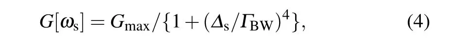
whereΔs=ωd/2-ωs,Gmax= 1+16κ2λ2/{κ2-4λ2+4(ωr-ωd/2)2}2, andΓBW=κ/(2G1/4max). Such broadened lineshape comes as higher order approximation of Taylor expansion for Eq.(2),due to the enlargedκ/2π=0.49 GHz.

Fig.2. Photos of the vacuum-gap-based lumped element Josephson parametric amplifier. (a) An optical image of the whole structure, which is characterized in this paper. The circuit components are individually colored and labeled. Port 1 is made for microwave signal,including probe tone and direct pump tone.Port 2 is made for both microwave signal and direct current input,thus allowing flux pump and on-chip bias. (b) A SEM image of the whole vacuum-gap-based structure and SQUID.The lighter larger rounds are standing contacts to support the floating pad. The darker small holes are made for removing the sacrifice layer during fabrication. (c)A SEM image of partial lumped capacitor,which serves as a proof of the quasi-floating condition. (d)A SEM image of the fabricated SQUID.
3. Design and fabrication
The structure of our LJPA is composed of lumped element part,CPW-based impedance transforming part,and control line. The lumped element part is composed of vacuumgap-based capacitor and SQUID.The control line is designed to allow both microwave pump and flux bias.
Fabrication process[32,36]is illustrated in Fig.3. On-chip lumped capacitor pad,control line and impedance engineering part are firstly patterned via photo lithography and dry etching from a niobium sputtered silicon substrate. Standing contacts of the lumped capacitor are separated from the on-chip ground by concentric ring gaps. CPW-based impedance transformer and SQUID are directly connected to the quasi-floating pad through standing contacts. Then we use e-beam lithography followed with double angle evaporation and in-chamber oxidation to fabricate the Josephson junctions. Another round of photo lithography is applied to reserve standing contacts between the on-chip ground and the quasi-floating capacitor pad.The photon resist(thickness about 3µm)used here serves as sacrifice layer.The quasi-floating capacitor pad is then formed by aluminum evaporation, and is separated from the on-chip one by initially etched gaps. Wet etching after third round of photo lithography is taken, to remove photon resist sacrifice layer and unwanted aluminum part. Both standing contacts and top layer etched holes are designed as regular hexagon nested array.

Fig. 3. Fabrication process for the vacuum-gap-based JPA. The circuit element sizes are distortedly plotted for illustrations. Material types are marked by different colors and annotated.
4. Measurement and results
Our characterization measurement is taken at 25 mK in a dilution refrigerator. Weak probe tone with characteristic frequency ofωs,is injected by the network analyzer through port 1. It experiences attenuation before reaching to the cryogenic environment. A circulator is placed in front of port 1. The pump tone is applied by signal generator through port 2. Mixing process transfer energy from the strong pump tone to the weak probe tone. The amplified probe tone then comes out,together with the idler tone and noise, through the circulator.The flux bias on the SQUID loop is controlled by global coil inside the magnetic shield,which can be replaced by flux input through on-chip control line, together with flux pump, using bias-tee. Spectrum analyzer is added into the output channel,to analyze the device noise performance.
Firstly,we modulate JPA characteristic frequency by applying flux to the SQUID loop through an external coil. Flexibility of circuit characteristic frequency allows Gigahertzrange operational bandwidth. As is illustrated in Fig. 4, gain region is not restrict to the frequency of CPW transformer,because its coupling to both environment and JPA is strong.However, expansion of gain bandwidth for signal dispersive fromωauxis weakened.

Fig. 4. Bias-dependent reflection spectrum. (a) Unpumped phase spectrum for varied bias. Orange dash line is the characteristic frequency fitting of the CPW transformer dressed JPA circuit. Φ0 refers to flux quanta. Three biased points are marked in blue, green, and purple. Their accordingly three wave mixing stimulated gain spectrum is plotted below. (b)The blue spectrum is pumped at 11 GHz,and biased at-0.293Φ0. The green spectrum is pumped at 12.18 GHz, and biased at 0.404Φ0. The purple spectrum is pumped at 13 GHz,and biased at-0.292Φ0.
We then focus on bias at 0.404Φ0, to characterize performance of the device. Under the pump tone with frequency of 12.18 GHz and power of-108 dBm, we obtain over 20-dB gain with 162-MHz bandwidth. The corresponding 1-dB compression is about-123 dBm. Measurement results indicate the capability for simultaneous multi-qubit readout.Note that all amplitudes of input signals are described in the amount before reaching sample box. Dynamic range and gain bandwidth of the device can be optimized by adjusting size of the vacuum-gap-based capacitor.[37]If size of the vacuumgap-based capacitor is halved, which results in halvedCvgb,similar to the JPAs with dielectric layer based parallel-plate capacitor,[31]gain bandwidth should be broadened beyond 300 MHz. Meanwhile, dynamic range should be decreased for the same nonlinear cavity frequency targeted design.[33]
We then compare the spectrum analyzer detected signal to noise ratio (SNR) under pumped and unpumped cases, for which subplot in Fig.5(d)serves as an example. With accordance to the characterized input channel attenuation and gain response(exactly the blue line in Fig.5(c)),this gives the JPA noise.

Fig. 5. LJPA performance characterization under pump condition of 12.18 GHz,-108 dBm. (a)Gain response evolution toward saturation along growing probe tone amplitude,for series probe frequencies. Probe frequency dependent 1-dB compression is plotted as gray dash line. (b)Detailed plot of the left one, for probe frequency at 6.09 GHz, with marked 1-dB compression at -123 dBm. (c) Gain response for probe power at -146 dBm (blue line)and-123 dBm(red line). Gray dash line represents gain response lineshape fitting. (d)Measured JPA noise(dots),with 1.2-dB insertion loss error colored in gray, and orange dash line indicating quantum limit. Frequencydependent noise photon number is transferred into noise temperature via¯hω/kB.Processing of SNR,at input signal frequency of 6.04 GHz,is taken as an example(circled in pink). Its original data(Qout[τ]=∫1/2τ-1/2τP[Δps]dΔps)zoomed in 5 kHz span is presented in the subplot,where the pink area refers to integration period τ (1/3.75 kHz),and Δps refers to frequency difference between probe tone and swept signal tone. T is the sufficiently settled integration period for wideband fast Fourier transformation that covers the JPA gain bandwidth (1/100 kHz). Red line refers to the pumped spectrum, and purple line refers to the unpumped spectrum. SNR is thus concluded from Qout[τ](T-τ)/{τ(Ntot[T]-Qout[τ])},where Ntot[T]=∫1/2T-1/2T P[Δps]dΔps.
To be specific, we can have a system noise in unit of quanta defined as
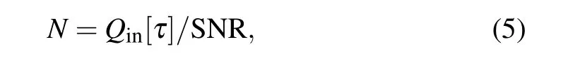
where footlabel‘in(out)’onQ[τ]refers to signal photon number input(output)during an integration period ofτ,and SNR represents signal to noise ratio detected by the frequency spectrum analyzer. It is worth-noting that integration period influence little on the noise calculation, because it is contained both in numerator and denominator of SNR. When JPA is not pumped,
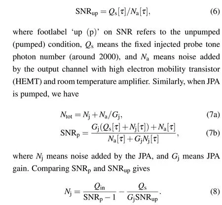
This thermal calibration source free method well matched the widely taken approximation method,where the noise is expressed asTJPA[ω]=Ttot[ω](1/ηSNR[ω]-1/G[ω]).[22]In this formula,Ttot(JPA)means the total(JPA)added noise in the temperature scale,ηSNRmeans SNR improvement, andGmeans JPA gain.Noise measurement results confirm that the vacuumgap-based structure reaches quasi quantum-limit.
5. Conclusion
For rounds of cooling, robustness of the vacuum-gapbased geometric structure has been verified.We also varied the gap design to test their room temperature capacitance, which turns to have parallel-plate-capacitor-equivalent linear dependency on size. This confirms designability of the electrical parameters.
In summary, we have proposed a vacuum-gap-based capacitance structure for fabricating low-noise lumped element JPA, with single material evaporation method. Our JPA achieves over 20-dB gain with 162-MHz bandwidth, with added noise about 1 quanta. The circuit can be further optimized by finite impedance engineering and smaller capacitor.Our device offers application in single-shot readout of multiqubit system,which emerges with the coming NISQ era.
Toward future integrated superconducting quantum circuits, air-bridge is becoming an essential component. Due to the fabrication compatibility, our vacuum-gap-based LJPA can be a strong candidate for hardware-efficient on-chip amplification. The vacuum-gap-based structure also inspires 3D-architectures of superconducting circuits. Furthermore,such capacitor with low parasitic inductance can play roles in lumped element circuit to tailor local electric field distribution,which offers flexibility on designing characteristic frequency and coupling strength.
Acknowledgements
Project supported by the National Key Research and Development Program of China(Grant No.2016YFA0301200),the National Natural Science Foundation of China (Grant Nos.62074091,12004044,and U1930402),the Science Challenge Project(Grant No.TZ2018003),the Fund from the New Energy and Industrial Technology Development Organization(Grant No. JPNP16007), and Japan Science and Technology Agency (Moonshot R&D, Grant No. JPMJMS2067 and CREST,Grant No.JPMJCR1676).
猜你喜欢
杂志排行

Chinese Physics B的其它文章
- Superconductivity in octagraphene
- Soliton molecules and asymmetric solitons of the extended Lax equation via velocity resonance
- Theoretical study of(e,2e)triple differential cross sections of pyrimidine and tetrahydrofurfuryl alcohol molecules using multi-center distorted-wave method
- Protection of entanglement between two V-atoms in a multi-cavity coupling system
- Semi-quantum private comparison protocol of size relation with d-dimensional GHZ states
- Probing the magnetization switching with in-plane magnetic anisotropy through field-modified magnetoresistance measurement