Construction and mechanism analysis on nanoscale thermal cloak by in-situ annealing silicon carbide film
2022-01-23JianZhang张健HaoChunZhang张昊春ZiLiangHuang黄子亮WenBoSun孙文博andYiYiLi李依依
Jian Zhang(张健), Hao-Chun Zhang(张昊春), Zi-Liang Huang(黄子亮),Wen-Bo Sun(孙文博), and Yi-Yi Li(李依依)
School of Energy Science and Engineering,Harbin Institute of Technology,Harbin 150001,China
Keywords: nanoscale thermal cloak,silicon carbide,molecular dynamics,in-situ annealing
1. Introduction
In 2008, Fanet al.[1]proposed transformation thermotics with reference to transformation optics, and introduced the concept of metamaterials into the field of thermotics, also known as thermal metamaterials. After they predicted the thermal cloak, researchers have designed a series of thermal cloak,[2-9]and other thermal functional devices are also designed, such as thermal concentrators,[10-12]thermal illusions,[13-16]thermal camouflage,[17-23]thermal rotations,[9,24]and macroscopic thermal diodes.[25,26]Thermal cloak as a typical representative of thermal functional devices has attracted extensive interest from researchers. Hanet al.[3]and Xuet al.[7]almost simultaneously designed a thermal cloak by the scattering cancellation method based on effective medium theory. Compared with the coordinate transformation method,the thermal cloak designed by this method is isotropic.
At the nanoscale, due to the wave-particle duality of phonons,some thermal functional devices have also been designed,such as quantum thermal rectification[27-30]and topological phonon Hall effect.[31]Nanoscale thermal cloaks with the same function as macroscopic thermal cloaks have also been developed. Yeet al.[32]designed a chemically functionalized graphene thermal cloak, and Liuet al.[33]designed an in-situ annealed silicon film thermal cloak by the “melt and quench” technique. Choeet al.[34]developed a platform for ion-write microthermotics (IWMT), first observed the phenomenon of cloaking at the nanoscale.
Existing nanoscale thermal cloaks are mostly constructed by graphene and crystalline silicon, while silicon carbide, as a representative of third-generation semiconductor materials,has splendid properties, such as the high thermal conductivity and the high wear resistance. It is suitable for aviation aerospace, automotive, and nuclear industries. In the present study, we construct a nanoscale thermal cloak based on silicon carbide. Besides,we quantitatively measure the perturbation of the existence of cloaking devices to the external environment by response temperature. Moreover,considering that the cloaking effect of the nanoscale thermal cloak is generated from the reduction in thermal conductivity due to phonon localization in the functional area, the potential mechanism of the designed cloak studied by calculating and analyzing the PDOS and MPR within the structure. This study extends the preparation method of nanoscale thermal cloaks and can provide a reference for the development of other nanoscale devices.
2. Molecular dynamics
We use the LAMMPS packages[35]to conduct the nonequilibrium molecular dynamics (NEMD) simulations. The potential of Tersoff is used to denote the interatomic interactions of Si and C atoms in the film,which can be expressed as follows:[36]
whereEdenotes the total energy of the system,iandjrepresent the atoms of the system,ri jdepicts the distance between atomiand atomj.fArepresents the potential of attractive pair,fRdenotes the potential of repellent pair,fCis just a smooth cutoff function aimed to limit the range of the potential. Thebi jis used to measure the bond order.
We use the macro classic model to establish the nanoscale thermal cloak in Fig. 1. Taking the unit cell (UC) as the basic unit, the number of UC inx,y, andzdirections are 60,40, and 2 respectively, where the lattice constant of silicon is 4.38 ˚A.The nanoscale thermal cloak is divided into four areas,the fixed area, the thermostat area, the background area, and the functional area. The functional area is the amorphous silicon carbide obtained after annealing,and the rest area is crystalline silicon carbide. The fixed area is the two ends along thexdirection with the length of 2 UC,to prevent the whole system from moving. The thermostat area consists of two parts,the hot bath,and the cold bath,each the length of which alongxdirection is 8 UC,as shown in Fig.1. In the thermostat area all the atoms are kept at high and low temperature respectively at both sides by Nose-Hoover thermostats[37]
wherepi,mi,Fidenotes the momentum, mass, and force of atomirespectively,γandτare the dynamic parameters and relaxation times of the thermostat,Nis the atomic number of the thermostats,andkBis the Boltzmann constant.
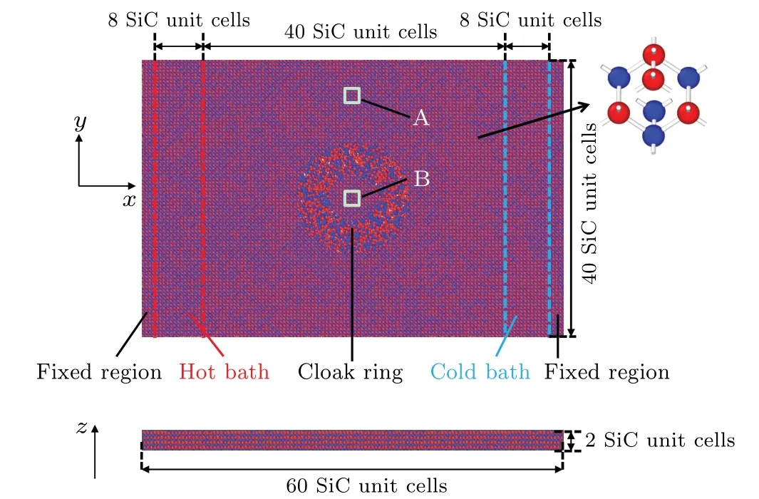
Fig.1. Schematic diagram of the system consisted of the nanoscale thermal cloak and the external environment. The environment contains three parts:fixed region,hot bath,and cold bath.
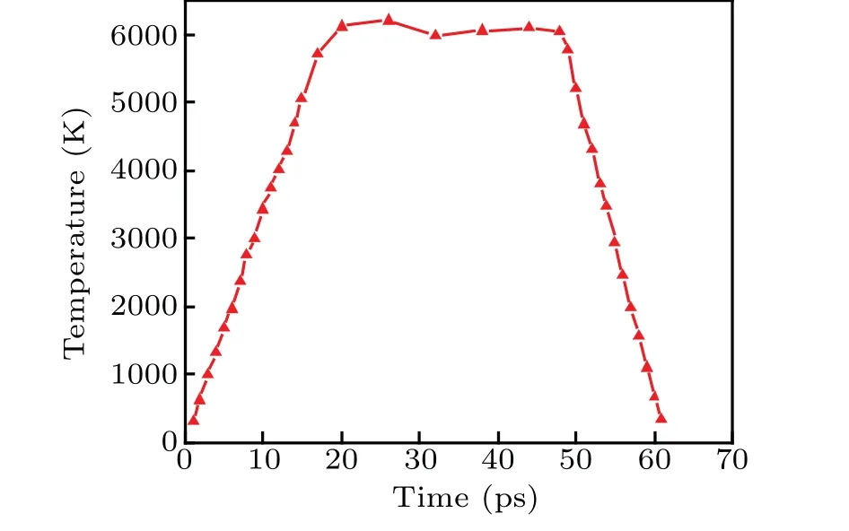
Fig. 2. Temperature variation during annealing in the ring region of the nanoscale thermal cloak.
The functional area is constructed by amorphizing crystalline silicon carbide with reference to the treatment of crystalline silicon amorphization. Periodic boundary conditions are used in all directions with a time step of 1 fs. At the beginning of the simulation,the left and right ends of the silicon carbide film are fixed to prevent it from moving. Then, all atomic velocities except those in the fixed region are set to the values corresponding to 300 K and obey the Gaussian distribution. The system is relaxed for 1000 ps in the NVT ensemble and the energy minimization process is stopped when all components of the force on the atoms are smaller than 10-3eV/˚A.The functional area is heated from 300 K to 6000 K at a rate of 2.85×10¹⁴K/s and maintained at 6000 K for a period of time to melt the silicon carbide crystals. Then the temperature is rapidly quenched to 300 K.At this time,the functional area has changed from the crystalline state to the amorphous state.The temperature change of the functional area during this process is shown in Fig. 2. In this way, 1 nm (inner radius of 25 ˚A and outer radius of 35 ˚A)and 2 nm(inner radius of 15 ˚A and outer radius of 35 ˚A) rings are constructed, respectively.Afterward,the NEMD simulation is performed. First,the energy is minimized again, then all atoms except those in the fixed region are given an initial velocity. After that, the system is placed in the NVT ensemble to equilibrate for 100 ps at 300 K. Finally, the temperature of the cold bath is set at 250 K, and the temperature of the hot bath is fixed at 350 K.Except for the fixed and the bath region, the entire system is simulated for 1000 ps in the NVE ensemble. The temperature and heat flux of the system are calculated,and the equation for calculating the temperature of each atom can be described as

whereεidenotes the kinetic energy of the atomi, dim is the dimensionality of the simulation and we set dim=3,Nrepresents the atomic number,kBis the Boltzmann constant. The equation calculating heat flux can be expressed as
whereJdenotes the heat flux,eiis the total energy each atom,Sidenotes the stress tensor each atom, and it has 9 components:xx,yy,zz,xy,xz,yx,yz,zx,zy.videnotes the velocity vector each atom.Vdenotes the volume of this area. The heat flux in three directions can be described by
3. Results and discussion
In Fig.1,we define two regions A and B,where B is located in the cloaking area. To evaluate the thermal cloaking performance, we first calculate the ratio of thermal cloaking(RTC):
whereJis the average heat flux, A and B are calculated regions.
The calculation results of RTCs are shown in Fig.3. The amorphous silicon carbide film has realized the control of the heat flux,so that the heat flux bypasses the functional area to achieve thermal cloaking,and the larger the width of the amorphous region,the better the cloaking effect.
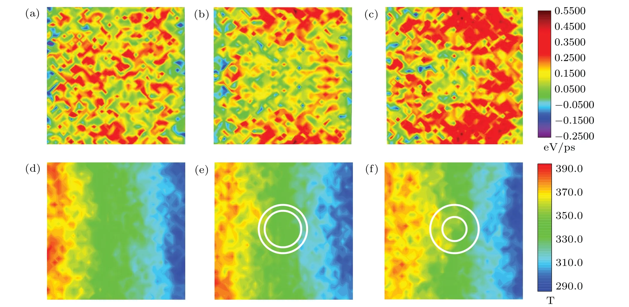
Fig.4. The heat flux and temperature distribution at different cloak ring widths at 400 ps: (a)-(c)the perfect film,1-nm cloak ring and 2-nm cloak ring heat flux distribution,respectively;(d)-(f)the perfect film,1-nm cloak ring and 2-nm cloak ring temperature distribution,respectively.
The single-atom heat flux is calculated by referring to the calculation method of Chenet al.[38]At the nanoscale heat flux is generated due to the motion of individual atom,but we are not concerned with the motion of individual atom. We chunk the computational domain,compute the average heat flux and average temperature within each chunk,and plot the heat flux and temperature distribution, as shown in Fig. 4. The silicon carbide film with cloaking structure produce the cloaking phenomenon. Besides, it can be experimental verified by referring to the platform for ion-write microthermotics(IWMT)designed by Choeet al.[34]It is proved that the amorphous structure can impede the flow of heat flux,and the reason for this is the reduced thermal conductivity of the amorphous structure.In addition,the cloaking phenomenon becomes more obvious as the width of the amorphous region increases. However, it is difficult to evaluate the disturbance to the external environment in the presence of the functional area,and for this reason further analysis is performed by calculating the response temperature(Tre):
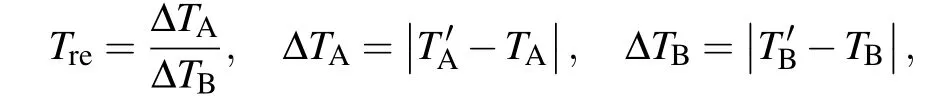
whereTdenotes average temperature of the perfect silicon carbide film,T′represents average temperature of the film with cloak, A and B indicate calculated regions. The main function of the thermal cloak is to make the heat flux bypass the functional area,thus protecting the functional area from the external environment,so the functional area remains low temperature, indicating that the smaller the response temperature value is, the better cloaking. For this purpose, the response temperature is calculated under different widths of cloak ring,as shown in Table 1. When the width of the amorphous area is 2 nm,the response temperature is the smallest,which indicates the impact on the external temperature field is minimal at this time. To further investigate the effect of inner and outer radius size on the cloaking performance,we separately fix the inner and outer radius to construct two ring(1 nm(inner radius of 15 ˚A and outer radius of 25 ˚A) and 2 nm (inner radius of 25 ˚A and outer radius of 45 ˚A))for calculation,and results are shown in Table 2.
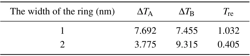
Table 1. ΔTA,ΔTB,Tre under different widths of the ring.

Table 2. RTC,Tre under different radius of the ring.
The smaller the inner radius, the better the cloaking effect; the larger the outer radius,the greater the disturbance to the external temperature. In addition,the cloaking effect is related to the size of the whole system, but as the amorphous region becomes larger,the cloaking effect increases.
To investigate the cloaking mechanism, we calculate the PDOS in the ring area. Besides, to control the same region variables, the ring regions we use to calculate PDOS in three structures are the same. Therefore, we take the cloaked domain of 2-nm ring as the standard, and we also calculate the PDOS in the inner and outer radius 1-nm ring respectively.The PDOS can be expressed as follows:
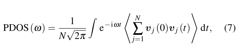
wherevjdenotes the velocity vector of atomj,Nrepresents the total number of atoms of the system,ωis the frequency of phonon. Figure 5 shows the PDOS of the atoms in the selected standard domains. In the perfect film,there is a strong peak at 27 THz and 75 THz respectively, which is consistent with previous studies.[39]While for the film with cloak ring,the amorphous silicon carbide atoms have a lower vibrational frequency, resulting in a weaker peak at the high-frequency region and an increase in the modulus at the low-frequency region. It can be observed the amorphous ones show a large number of modes from 20 THz to 80 THz. Compared with the outer radius interface, the inner radius interface has a greater impact on PDOS, not only the peak is reduced, but the frequency of the peak also shifts. The main reason is that the proportion of amorphous silicon is larger than that of the 1-nm ring at the inner radius interface compared to the outer radius interface.

Fig.5. Results of PDOS:(a)different ring widths;(b)inner radius interface;(c)outer radius interface.
To analyze the differences in PDOS,we further calculate the MPR[40,41]
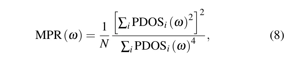
where PDOSi(ω)denotes the local density of states ofith according to Eq. (7),Ndenotes the total number of atoms in the system. The MPR of perfect silicon carbide film and silicon carbide film with cloaking structure is shown in Fig. 6.Compared with the perfect silicon carbide film, the MPR of the low-frequency phonons and high-frequency phonons of the silicon carbide film with a cloaking structure has been significantly reduced. For perfect silicon carbide films, most of the MPRs are above 0.5, which means that these phonon modes have been decentralized. However, the MPRs of silicon carbide films with cloaking structures are all lower than 0.5,which means the localization of the phonon mode.[42]The results confirmed that the localization of phonons is the cause of the decrease in the thermal conductivity of amorphous silicon carbide.Since only half of the silicon carbide atoms in the 1-nm ring region are composed of amorphous silicon carbide,the rest are crystalline silicon carbide,and the atoms in the 2-nm ring region are all composed of amorphous silicon carbide,both MPRs of films with cloak of different sizes are lower than that of the perfect case, leading to the stronger phonon localization.The MPR of the 1nm ring at the inner and outer radius interface is similar, but the MPR of the 1nm ring at the inner radius interface is slightly lower, indicating that the inner radius interface has a greater contribution to the cloaking performance.In short,the appearance of cloaking is related to the localization of phonons in the specific region.The stronger the localization,the better the thermal cloaking performance.

Fig.6. Results of MPR:(a)different ring widths;(b)inner radius interface;(c)outer radius interface.
4. Conclusion
In summary, we construct a nanoscale thermal cloak based on silicon carbide film, and the functional area is constructed by transforming crystalline silicon carbide into amorphous through the “melt and quench” technique. First, the cloaking performance of the constructed nanoscale thermal cloak is explored by calculating the ratio of thermal cloaking, and it is proved that the amorphous silicon carbide film can also realize the regulation of the heat flux,so that the heat flow can bypass the functional area. Then, by drawing the distribution of heat flux and temperature,the existence of thermal cloaking phenomenon is confirmed. And the heat transfer around the functional area of the nanoscale thermal cloak is consistent with the heat transfer around the functional area of the macro thermal cloak. In addition, the disturbance of the external temperature field caused by the existence of the cloaking structure is analyzed by the response temperature. Results show that the smaller the inner radius, the better the cloaking effect; the larger the outer radius, the greater the disturbance to the external temperature;but as the amorphous region increases the cloaking effect increases. Finally, through the phonon localization theory, the reason for the decrease of the thermal conductivity of the functional region is explained,and the potential mechanism of the nanoscale thermal cloak is discussed by calculating PDOS and MPR.The main reason that reduces the thermal conductivity of amorphous silicon carbide is phonon localization.The stronger the localization,the lower the thermal conductivity. Moreover,the inner radius interface contributes more to the cloaking performance than the outer radius interface. Our research has expanded the methods of building nanoscale thermal cloaks,and lays the foundation for the research of new nanoscale thermal functional devices.
Acknowledgement
Project supported by the National Natural Science Foundation of China(Grant No.51776050).
猜你喜欢
杂志排行

Chinese Physics B的其它文章
- Superconductivity in octagraphene
- Soliton molecules and asymmetric solitons of the extended Lax equation via velocity resonance
- Theoretical study of(e,2e)triple differential cross sections of pyrimidine and tetrahydrofurfuryl alcohol molecules using multi-center distorted-wave method
- Protection of entanglement between two V-atoms in a multi-cavity coupling system
- Semi-quantum private comparison protocol of size relation with d-dimensional GHZ states
- Probing the magnetization switching with in-plane magnetic anisotropy through field-modified magnetoresistance measurement