Brightening single-photon emitters by combining an ultrathin metallic antenna and a silicon quasi-BIC antenna
2022-01-23ShangtongJia贾尚曈ZhiLi李智andJianjunChen陈建军
Shangtong Jia(贾尚曈) Zhi Li(李智) and Jianjun Chen(陈建军)
1State Key Laboratory for Mesoscopic Physics,School of Physics,Peking University,Beijing 100871,China
2Department of Physics and Applied Optics Beijing Area Major Laboratory,Beijing Normal University,Beijing 100875,China
3Collaborative Innovation Center of Extreme Optics,Shanxi University,Taiyuan 030006,China
4Frontiers Science Center for Nano-optoelectronics&Collaborative Innovation Center of Quantum Matter,Peking University,Beijing 100871,China
5Peking University Yangtze Delta Institute of Optoelectronics,Nantong 226010,China
Keywords: single-photon emitters,brightness,hybrid nanostructures,ultrathin metallic antenna,quasi-bound state in the continuum(BIC)
1. Introduction
Single-photon emitters (SPEs) are the fundamental components in many quantum applications,[1]such as quantum key distributions,[2,3]quantum circuits,[4,5]boson sampling,[6,7]and quantum precision measurement.[8]For most quantum applications, a high brightness of SPEs with sufficient emission photons is essential.[1,9]By enlarging Purcell enhancements (Purcell factor Fp) as well as increasing quantum yields(QY)and collection efficiencies(CE)of SPEs,the brightness of SPEs could be increased.[9-13]In the past decades, enormous efforts were made to increase the brightness of SPEs. For example, by designing dielectric slot waveguides[14]or dielectric nanoparticles,[15]the Purcell factors were approximately Fp=300.0[14]and Fp=62.0,[15]respectively. By employing metallic bowtie antennas,[16]dimer antennas,[17]plasmonic nano-focusing cavities,[18]and a plasmonic waveguide-slit structure,[19]the Purcell factors were predicted to be from 1.5×10³to 1.7×10⁵[19]due to subwavelength field confinements of surface plasmons (SPs).However, the quantum yields in metallic nanostructures are usual very small (< 0.2)[19]because of the huge losses of metals. On the contrary, the quantum yields in the dielectric structures were easier to achieve a high quantum yield(>0.66).[21,22]In terms of collection efficiencies, parabolic antennas,[23]Yagi-Uda antennas,[24]bull’s eye antennas,[25,26]and band structures[27]were designed to control the radiative direction,and the collection efficiencies were predicted to be 0.6[numerical aperture(NA)=0.5],[23]0.84(NA=0.5),[24]0.95(NA=1.2),[25,26]and 0.99(NA=1.2),[27]respectively.
Recently,many metallic nanostructures were designed to enlarge both of Purcell enhancements and quantum yields of SPEs.[10,28,29]For example, by designing a metallic nanorod and a metallic film (with a dielectric gap ofgd= 5 nm),Fp≈3.0×10³and QY≈0.30 were numerically predicted.[28]By using a metallic torus antenna placed on a metallic film with a dielectric gap (gd=5 nm), Fp≈1.2×10⁴and QY≈0.30 were numerically predicted.[10]By utilizing a metallic nanorod-nanorod structure(gd=10 nm),Fp≈4.1×10⁴and QY≈0.32 were numerically predicted.[29]In these metallic structures,[10,28,29]the Purcell factors were enhanced by the SP gap modes,which had tiny mode volumes and huge local density of states, in metal-insulator-metal (MIM) structures.[20]The quantum yields were increased by the nanorods or tori,[10,28,29]which scattered the energy from the MIM structures and thus reduced the losses in metals.[10,28,29]However,the quantum yields of the above structures were still small(QY≤0.32).[10,28,29]Therefore,in metallic nanostructures,it was still a huge challenge to increase both of Purcell enhancements and quantum yields of SPEs simultaneously. Moreover,the radiation fields of SPEs almost spread along the surface of metals or diverged in the far field with a large angle,and these works did not consider the collection efficiencies.[10,28,29]
To increase all of Purcell enhancements,quantum yields,and collection efficiencies of SPEs, hybrid dielectric-metal structures were proposed.[30-33]These hybrid dielectric-metal nanostructures combine the advantages of both dielectric nanostructures(high quantum yields)and metallic nanostructures (high Purcell enhancements). For example, by putting a silicon nano-patch on a metallic nanoparticle-on-mirror(NPOM)structure(gd=30 nm),Fp≈1.5×10²,QY≈0.75,and CE≈0.99 were numerically predicted;[30]By combining a metallic bowtie antenna with silicon Yagi-Uda antennas,Fp≈1.8×10³, QY≈0.60,and CE≈0.95 were numerically predicted;[31]By combining a gold nanorod with a silicon nano-disk(gd=5 nm), Fp≈1.4×10³, QY≈0.70, and CE≈0.90 were numerically predicted.[32]Lately, a silicon cylinder was placed on a metallic film(gd=2 nm,tm=∞),[33]Fp≈5.0×10³,QY≈0.75,and CE≈0.60 were numerically predicted.[33]In the above works,[30-33]the Purcell enhancement was enlarged by the subwavelength field confinements of the NPOM structures,[30]bowtie antennas,[31]nanorods,[32]and the metallic film.[33]The quantum yields (QY≥0.60)were increased by high-index silicon antennas because the ratio of electromagnetic fields in metals became smaller.[30-33]The collection efficiencies were increased by the resonant modes of silicon antennas,[30-33]whose divergence angles of emission light were smaller than 30°.
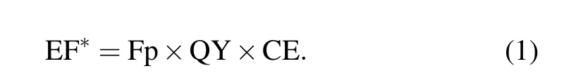
To evaluate the total effects of three factors on brightness of SPEs in nanostructures,an enhancement factor(EF*)is defined by
The largest EF*in the above nanostructures[30-33]is EF*≈2.2×10³.[33]Due to the large mode size(~λ)of surface plasmon polaritons on the bulky metals,the Purcell enhancement of the bulky bowtie antenna mainly depends on the gap size of the bowtie antenna.[16]What’s worse,the Purcell enhancements (Fp≤5.0×10³) of these hybrid nanostructures[30-33]are much smaller than those (Fp≤4.1×10⁴) of metallic nanostructures[10,28,29]because the silicon antennas of the above hybrid nanostructures make the SPP field confinements poorer. Hence,quantum yields of hybrid nanostructures[30-33]increased at the huge expense of Purcell enhancements. It is still a big challenge to realize a much larger EF*in hybrid nanostructures to significantly brighten SPEs.
2. Proposal and simulation
In this paper,we propose to combine an ultrathin metallic bowtie antenna with a silicon antenna (Fig. 1) to greatly enhance the brightness of SPEs. The ultrathin metallic bowtie antenna is placed above a metallic film with a gap,and its detail is shown in the inset of Fig.1. The rectangular coordinate system is also given by the inset.Thexyplane is on the middle surface of the ultrathin metallic bowtie antenna with thex-axis parallel to the bowtie antenna’s symmetry axis and thez-axis passing through the center of the gap. The origin of coordinatesOis located at the center of the bowtie antenna.
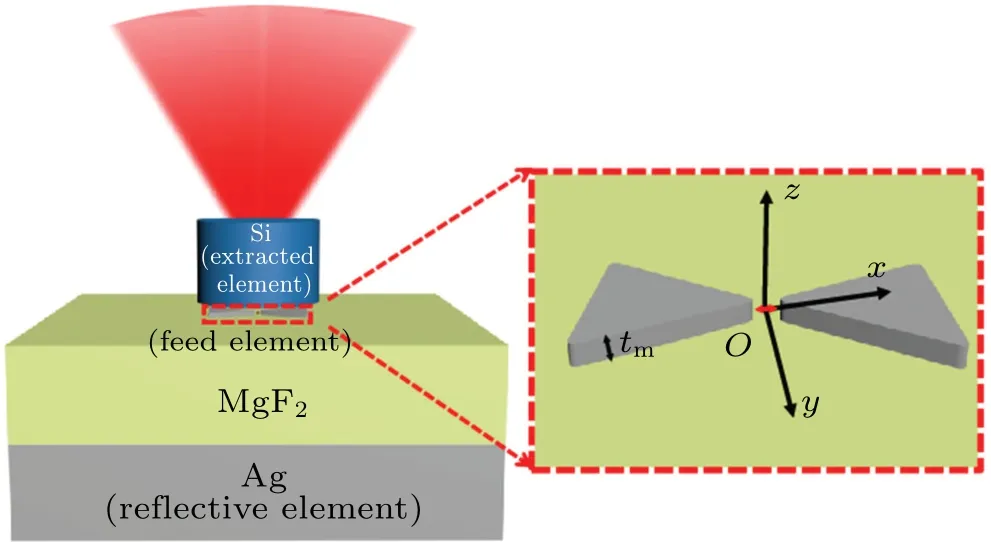
Fig. 1. Schematic of the overall hybrid structure. The structure is formed by three components:an ultrathin metallic bowtie antenna(Ag),a dielectric antenna(Si),and a thick metallic substrate(Ag).Inset shows the detail of the ultrathin metallic bowtie antenna. The rectangular coordinate system is added in the inset.
The ultrathin metallic bowtie antenna(with a thickness oftAg)is used to obtain a high Purcell enhancement due to its tiny mode volume of the resonant SPP mode. Herein, we choose an ultrathin bowtie antenna rather than a bulky one to improve the Purcell enhancement. The ultrathin metal film(<10 nm)supports an asymmetric SPP mode with deep-subwavelength field confinements (mode size~λ/100).[10,33]As a result,the Purcell enhancement of our nanostructure is predicted to be approximately two orders of magnitude greater than those based on bulky one.[10,33]The high-index silicon antenna under a quasi-BIC resonant state is used to obtain a high quantum yield by extracting the radiation field from the metallic bowtie antenna. Moreover,the silicon antenna shows small influence on the Purcell enhancement(only being decreased by 38%).
Due to the improvement of the radiation directivity by the quasi-BIC resonant mode and the constructive interference between the upward radiation and downward radiation reflected by the metallic film,the collection efficiency is also increased. As a result,the Purcell enhancement,quantum yield,and collection efficiency are predicted to be Fp≈2.6×10⁶,QY≈0.70,and CE≈0.71,respectively.The Purcell enhancement (Fp≈2.6×10⁶) in the proposed hybrid nanostructures is 63 times greater than those (≤4.1×10⁴) in the previous metallic and hybrid nanostructures.[10,28-33]Consequently,the enhancement factor of a SPE is calculated as EF*≈1.3×10⁶,which is 5.6×10²times greater than those(EF*≤2.2×10³)in the previous metallic and hybrid structures.[10,28-33]
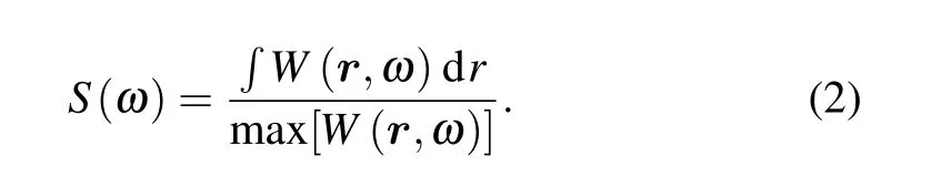
To understand the underlying physics in the hybrid structure,we first study the antisymmetric SPP mode supported in the ultrathin metallic film by the finite element method solver of COMSOL Multiphysics(mode analysis and frequency domains). The effective refractive index(neff)and mode size of the antisymmetric SPP mode versus the thickness of silver filmtAgare shown in Fig. 2(a). Herein, the metallic film is set as silver, and it is placed on an MgF2(nMgF2=1.38) substrate.The vacuum wavelength is 780 nm.[33]The medium above the silver film is set as air (nair=1). The permittivity of silver isεAg=-29.4+0.36i.[34]The mode size is obtained by a similar method from Ref.[35]by
With decreasingtAg,neffincreases and the mode size shrinks[Fig. 2(a)]. The reason is that the electromagnetic field of the antisymmetric SPP mode is confined more tightly with decreasingtAg.[36]WhentAg=2 nm, the electric field(Ez)distribution of an antisymmetric SPP mode is shown in Fig.2(b).The electromagnetic field is tightly confined on the silver film.WhentAg≤4 nm, the mode sizes are smaller than 1 nm[Fig. 2(a)], which is far smaller than the incident wavelength(λ=780 nm).
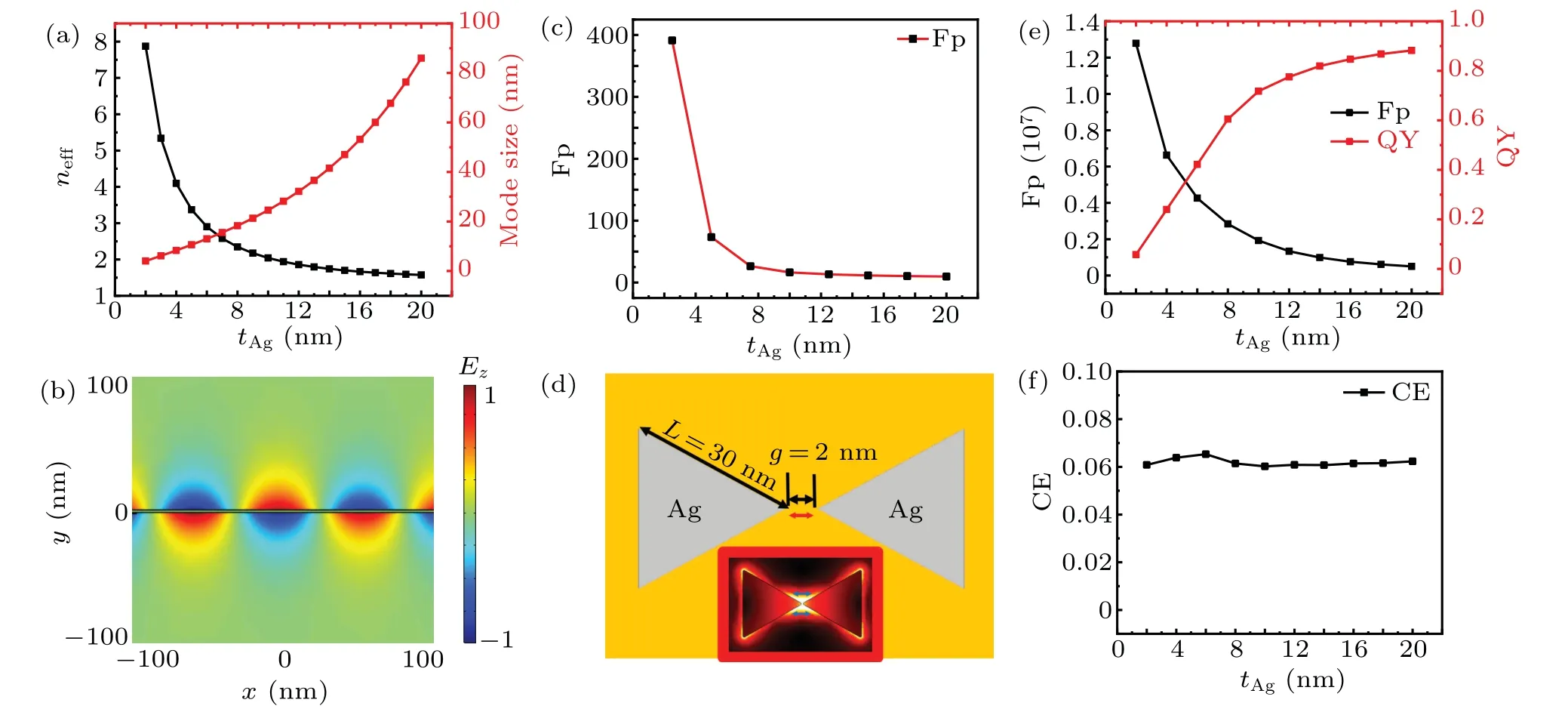
Fig.2. The(a)neff and mode size of a silver film versus tAg. (b)Electric field distribution of an antisymmetric SPP mode(tAg=2 nm)on the surface of a silver film. (c)Fp of a dipole placed 5 nm above a silver film versus tAg. (d)Schematic of the ultrathin metallic bowtie antenna placed on a MgF2 substrate. The red arrow denotes the orientation of the dipole. Inset: Electric distribution (|E|) of the bowtie antenna in xy plane. Blue arrows denote the polarization of the electric field in the gap. (e)Fp, QY and(f)CE of the dipole placed in the center of the ultrathin metallic bowtie antenna versus tAg.
Then, we calculate the Purcell enhancement of a dipole placed 5 nm above an ultrathin silver film with differenttAg[Fig.2(c)].In simulation,a dipole is used as a SPE.The dipole orients along thez-axis and its intrinsic quantum yield assumes to be 1.[1,10,28-33,37-41]The Purcell enhancement is calculated by[10,28,41]
whereγ0andW0are the total decay rate and the total power of a dipole placed in a vacuum, respectively.γtotalandWtotalare the total decay rate and the total power of a dipole placed in a structure,respectively.Wtotalcan be obtained by conforming the dipole in a 2 nm radius sphere and performing surface integrals over the Poynting vectorSon the sphere, and it is calculated by[28]

The Purcell enhancement shows a monotonous increase from 9.6 to 391.2 with decreasingtAgfrom 20 nm to 2 nm in Fig.2(c). The reason is that the mode sizes of the asymmetric SPP mode in the ultrathin metallic film become smaller whentAgdecreases[Fig.2(a)]. Fortunately,the ultrathin metal film(tmfrom 1 nm to 10 nm)has been realized in experiments,[42]so the choice of the 2-nm metal film is reasonable.
Next, we simulate an ultrathin metallic bowtie antenna placed on an MgF2substrate[Fig.2(d)]. The bowtie antenna has a thickness oftAg, a length ofl, and a gap ofg. In addition, the antenna’s edge is curved for 2 nm, which can avoid the tip bringing errors in the simulation. A plane wave,whose polarization orients along thex-axis,vertically illuminates the bowtie antenna(tAg=6 nm,l=30 nm, andg=2 nm). The tiny gap of the bowtie antenna(g=0.5 nm)has been realized by electron-beam lithography in the previous work.[43]The electric field|E|distribution is shown by the inset in Fig.2(d).The electric field|E|confined tightly in the gap is larger than that outside the gap. The electric field|Ex|in the gap is 2700 times larger than that of the incident plane wave.The polarization of the electric field in the gap is along thex-axis(denoted by the blue arrows), which verifies that the SPP mode of the metallic bowtie antenna resonates alongx-axis.
In the ultrathin metallic bowtie antenna with a dipole(orienting along thex-axis) placed in the middle of the gap, the Purcell enhancements,quantum yields,and collection efficiencies are simulated. The quantum yield is calculated by[10,28,41]
WhentAgdecreases, the Purcell enhancement and quantum yield are shown in Fig. 2(e). The Purcell enhancement is improved largely from 5.0×10⁵to 1.3×10⁷with decreasingtAg. The variation tendency stems from that the mode size of the asymmetric SPP mode in the ultrathin metallic film becomes smaller whentAgdecreases [Fig. 2(a)]. Due to the ultra-tight field confinements and enormous field enhancements of the resonant SPP mode in the metallic bowtie antenna[Fig.2(d)], the Purcell enhancement is enlarged. The Purcell enhancement(Fp≥4.2×10⁶)of the ultrathin bowtie antenna(tAg≤6 nm)is approximately two orders of magnitude larger than those(Fp≤4.1×10⁴)of the previous metallic and hybrid structures.[10,28-33]The quantum yield decreases rapidly(from 0.88 to 0.05) because losses in the metallic antenna increase when the mode size of the SPP mode becomes smaller in the thinner silver film[Fig.2(a)]. The quantum yields(QY≤0.4)of the ultrathin metallic bowtie antenna(tAg≤6 nm)are lower than those(QY≥0.6)of previous hybrid structures.[30-33]Besides, the collection efficiencies are very low [Fig. 2(f)] because the ultra-tight confinements by the ultrathin bowtie antenna suppress the energies radiating to far field [Figs. 2(a)and 2(b)]. The collection efficiency (CE≈0.06) of the ultrathin metallic bowtie antenna (tAg≤6 nm) is an order of magnitude lower than those (CE≥0.6) of previous hybrid nanostructures.[30-33]A thickness oftAg=6 nm is selected based on the balance between Purcell enhancement and quantum yield(Fp≈4.2×10⁶,QY≈0.40,and CE≈0.06).
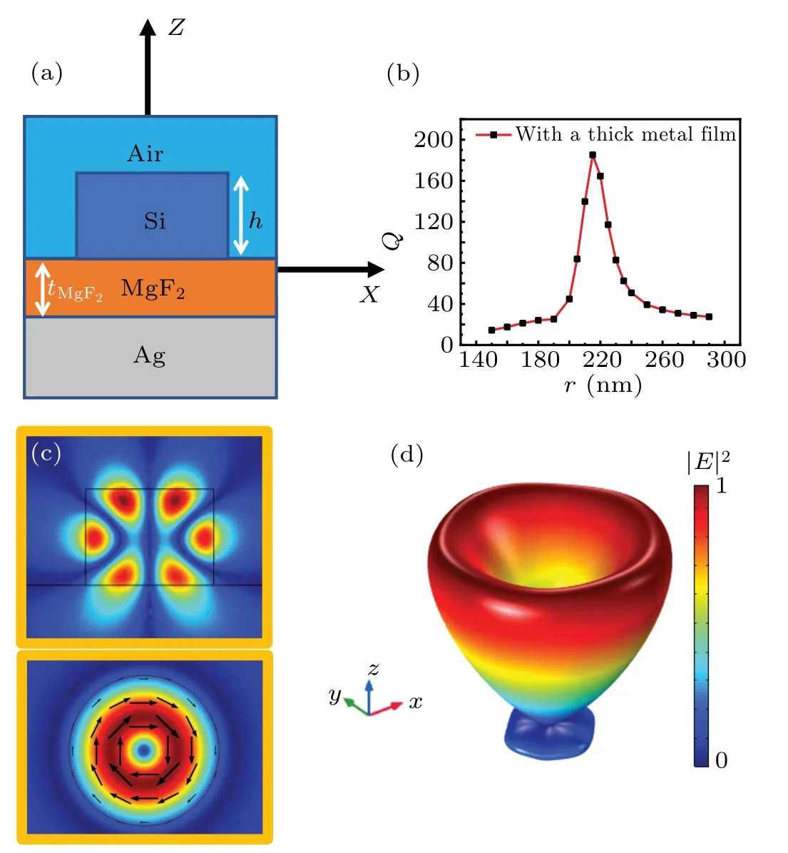
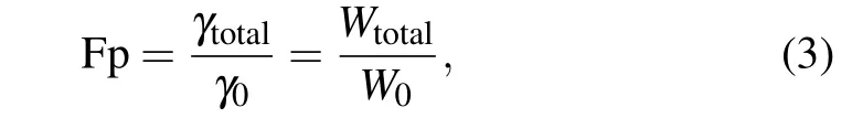
Fig. 3. (a) Front view of a silicon antenna placed above a silver film. (b)Optical quasi-BIC mode of an individual silicon cylinder in(a). The Q with a thick metal film versus r. Here,h=300 nm. (c)Electric field|E|distributions in the xz cross section(top)and xy cross section(bottom),respectively.The black arrows in bottom denote the electric filed polarization. (d) The 3D far field intensity of the silicon antenna at the quasi-BIC state.
To increase the quantum yield and collection efficiency,we propose to combine a high-index silicon (nSi=3.5) antenna to form a hybrid nanostructure, as shown in Fig. 3(a).Noting that the silicon antenna is quite small so that we ignore the absorption losses of silicon atλ=780 nm.Moreover,a silver substrate is placed below the silicon antenna separated by an MgF2spacer[with a thickness oftMgF2=250 nm], which is used to reflect the downward radiation from the quasi-BIC mode and forms constructive interference with the upward radiation. The quality factor(Q)versus different radii(r)of the silicon antenna is displayed in Fig. 3(b). Whenr=215 nm,theQof the silicon antenna arrives at a maximum, revealing a quasi-BIC state. The definition, principle, and calculation method of the quasi-BIC state can be found in Ref. [44]. In this case, the electric field|E| distributions in thexzandxycross sections of the silicon antenna are shown in Fig. 3(c).The electric vectors are denoted by black arrows in the bottom of Fig. 3(c). As a result, the quasi-BIC mode radiates an azimuthally polarized light.The three-dimensional(3D)far field intensity is shown in Fig.3(d). The silicon antenna under the quasi-BIC state radiates almost along the upper space,and the divergence angle is approximately 30°[Fig. 3(d)], indicating good radiation directivity.
At last,we insert the ultrathin metallic bowtie antenna between the silicon antenna and MgF2spacer. The orientation of the dipole is the same as that in Fig. 2(d) [along thex-axis].In addition,we separate the ultrathin metallic bowtie antenna and the silicon antenna by a MgF2layer (with a thickness ofd=2 nm),[33]as schematically shown in Figs.4(a)and 4(b).In the hybrid nanostructure,the silicon antenna can extract the confined electromagnetic field from the metallic bowtie antenna more easily due to its high refractive index. As a result,the ratio of electromagnetic fields in the ultrathin metallic bowtie antenna decreases, and the quantum yield increases.We move the silicon antenna along they-axis, and the simulated results are shown in Figs. 4(c) and 4(d). Herein, the dipole is always placed in the middle of the gap. In Fig.4(c),the Purcell enhancements increase (decrease) monotonously[from 1.4×10⁶(2.6×10⁶) to 2.8×10⁶(1.4×10⁶)] at the range ofy=20 nm-60 nm(160 nm-200 nm). And it changes gently at the range ofy=60 nm-160 nm because the resonant SPP mode of the metallic bowtie antenna overlaps with the quasi-BIC mode of the silicon antenna at the range ofy=60 nm-160 nm [Fig. 3(c)]. The quantum yields increase(decrease) monotonously [from 0.40 (0.70) to 0.70 (0.40)] at the range ofy=20 nm-110 nm(110 nm-200 nm). When the ultrathin metallic antenna is located aty=110 nm, the overlap between the metallic bowtie antenna and silicon antenna reaches at the maximum. The quantum yield is QY≈0.70,and the Purcell enhancement is Fp≈2.6×10⁶, which losses 38% from that (Fp≈4.2×10⁶) of the bare metallic bowtie antenna.
Fig.4. Schematic and characterization of the hybrid structure: (a)front view and(b)top view of the hybrid structure. The coordinate axes are the same as those in Fig. 1. Inset shows the detail of the ultrathin metallic bowtie antenna. Orientation of the dipole is added in (a). In (b),the moving direction of the silicon antenna is denoted by a white arrow. (c)Fp,QY,(d)CE,and EF* of the dipole placed in a hybrid structure versus y,(e)3D far field intensity at y=85 nm.
In Fig. 4(d), the collection efficiencies decrease slightly from 0.8 to 0.6. The enhancement factor is also calculated,as shown in Fig.4(d). The enhancement factors increase(decrease) at the range ofy=20 nm-85 nm (85 nm-200 nm).The maximal enhancement factor (EF*≈1.3×10⁶) is obtained aty=85 nm,and the 3D far field intensity is displayed in Fig. 4(e). The hybrid structure shows an excellent upward radiation characteristic, which is similar to that of Fig. 3(d).The lack of the cylindrical symmetry [Fig. 4(e)] results from that the ultrathin metallic bowtie antenna breaks the symmetry of the silicon antenna. Comparing with the previous work,[33]we overcome the challenge that the light energy confined on the ultrathin metal surface was difficult to be extracted by a dielectric antenna.[33]
The Purcell enhancement, quantum yield, and collection efficiency of our nanostructure are predicted as Fp≈2.6×10⁶,QY≈0.70, and CE≈0.71, respectively. The Purcell enhancement (Fp≈2.6×10⁶) is 520 times greater than those(Fp≤5×10³) in hybrid nanostructures,[30-33]and 63 times greater than those (Fp≤4.1×10⁴) even in previous metallic nanostructures.[10,28,29]Moreover, the quantum yield and the collection efficiency are close to those of the previous hybrid nanostructures.[30-33]The enhancement factor (EF*≈1.3×10⁶) is 5.6×10²times greater than the simulation and experimental results (EF*≤2.2×10³) in previous metallic and hybrid nanostructures.[10,25,28-33,45]By further optimizing the position of the silicon antenna and moving the location of the dipole along thez-axis,the enhancement factor is increased to be EF*≈1.8×10⁶.
In addition, the simulation shows that the Purcell enhancement of a dipole orienting along thez-axis ory-axis is smaller than that orienting along thex-axis by two orders of magnitude. The reason is that the electric field at the center of the bowtie antenna is along thex-axis. As a result,the dipole orienting along thez-axis ory-axis has little effect on the results. With the help of the recent nano-fabrication techniques,[42,43]the ultrathin metal film (tmfrom 1 nm to 10 nm) can be fabricated by an evaporation technique with a sputtered copper seed layer,[42]and the metal bowtie antenna with ultrathin gap(gfrom 0.5 nm to 10 nm)can also be fabricated by a developed high-resolution electron-beam lithography(EBL)process.[43]The silicon antenna and multilayer film can be fabricated by EBL and a dry-etching process.[44]The thickness accuracy on the metal film in Ref.[42]is 1 nm,and the gap accuracy on the bowtie antenna in Ref.[43]is 0.5 nm.Moreover, the silicon antenna has a loose diameter accuracy of±20 nm which is easy to be confirmed in EBL. When the thickness and gap of the ultrathin bowtie antenna and the radius of the silicon antenna reach their respective fabrication tolerances (e.g.,tAg=7 nm,g=2.5 nm, andr=225 nm),the simulation results show that the Purcell enhancement decreases by about 30%. Therefore,our structure is expected to be experimentally realized in the future.
3. Conclusion
We proposed to brighten SPEs by combining an ultrathin metallic bowtie antenna and a silicon antenna on a metallic substrate. The Purcell enhancement (Fp≈2.6×10⁶)in the proposed hybrid nanostructures is 63 times greater than those (≤4.1×10⁴) in the previous metallic and hybrid nanostructures.[10,28-33]The silicon antenna was used to keep a high quantum yield (QY≈0.70) and collection efficiency(CE≈0.71). Finally, the enhancement factor was calculated as EF*≈1.3×10⁶, which is 5.6×10²times greater than those (EF*≤2.2×10³) in the previous metallic and hybrid structures.[10,25,28-33,45]The bright SPEs might find important applications in the areas of quantum key distributions, quantum circuits,boson sampling,and quantum precision measurement.
Acknowledgements
Project supported by the National Key Research and Development Program of China(Grant Nos.2018YFA0704401,2017YFF0206103,and 2016YFA0203500),the National Natural Science Foundation of China (Grant Nos. 61922002,91850103, 11674014, 61475005, 11527901, 11525414, and 91850111), and the Beijing Natural Science Foundation,China(Grant No.Z180015).
杂志排行

Chinese Physics B的其它文章
- Superconductivity in octagraphene
- Soliton molecules and asymmetric solitons of the extended Lax equation via velocity resonance
- Theoretical study of(e,2e)triple differential cross sections of pyrimidine and tetrahydrofurfuryl alcohol molecules using multi-center distorted-wave method
- Protection of entanglement between two V-atoms in a multi-cavity coupling system
- Semi-quantum private comparison protocol of size relation with d-dimensional GHZ states
- Probing the magnetization switching with in-plane magnetic anisotropy through field-modified magnetoresistance measurement