Mode splitting and multiple-wavelength managements of surface plasmon polaritons in coupled cavities
2022-01-23PingBoFu符平波andYueGangChen陈跃刚
Ping-Bo Fu(符平波) and Yue-Gang Chen(陈跃刚)
School of Physics,Guizhou University,Guiyang 550025,China
Keywords: surface plasmon polaritons,coupled resonators,multiplexing
1. Introduction
Surface plasmon polaritons(SPPs)integrated circuits manipulate electromagnetic waves in subwavelength scale,[1,2]which are composed of many nanoscale elements, such as subwavelength plasmonic waveguides,[3,4]beam splitters and interferometers,[5]logic gates[6]and demultiplexer.[7]In highly integrated SPPs circuits,integrating various functional elements to one waveguide is needed. Metal-insulator-metal(MIM)waveguide has the advantages of deep-subwavelength confinement, low bend losses and easy integration.[8]The MIM waveguide is a good choice for SPPs integrated bus. Integrating all sorts of classical functional devices to the MIM bus waveguide is a key compatibility problem for highly integrated SPPs circuits. A simple scheme is proposed to solve the problem. In or near the MIM waveguide, various devices with classical functions are designed to manipulate the SPPs.
Fabry-Perot(F-P)cavity is a classical tool to manipulate the electromagnetic waves. A simple F-P cavity consists of two parallel flat mirrors with a space between them. Electromagnetic waves are reflected back and forth between two mirrors, and resonances form for special wavelengths in the cavity.The F-P cavities are used in many optical devices,such as filters, laser cavities, spectrometers and routings.[9]Similar to the classical F-P cavity, the cavities composed of the structural defects in photonic crystal can manipulate waves in wavelength scale and have wide range of applications.[10-12]The classical cavity-resonance principle can also be used to manipulate SPPs in subwavelength scale.The SPPs functional devices composed of metallic resonant cavities can confine SPPs to the volumes with dimensions considerably smaller than wavelength.[13,14]A spaser is proposed for surface plasmon laser in nanometer metallic cavities.[15,16]The couplings between metallic cavities and waveguides have been studied widely. Many interesting phenomena appear, such as optical electromagnetic induced transparency (EIT),[17,18]slow light[19,20]and Fano resonances.[21,22]Around MIM waveguide,metallic cavities are designed to realize some functions,such as filtering,[23]demultiplexing,[24]beam splitting and Mach-Zehnder interferometers.[25]Besides of SPP integration, the resonances in metallic cavities are also applied to nanosensors.[26-28]Many metallic coupled structures are studied. Multiple cascaded nanodisk structures are used to design slow light devices and optical switches.[29]The wide bandgap of transmission can be adjusted in the symmetrical multipleteeth-shaped structure.[30]A side-coupled cavity can realize wavelength selection and nano-sensing.[31]
Here multiple coupled cavities (CCs) are designed directly in MIM bus waveguide. The classical functions,such as filtering, demultiplexing and routing, can be realized through the resonances in the CCs. Compared to the cavities in dielectric structures, for example, photonic crystals,[10-12]the metallic CCs can overcome diffraction limitation and manipulate SPPs in subwavelength scale. In contrast to the metallic coupled structures,[23-25,29-31]the CCs designed in waveguide are more compact and easy to be integrated. The coupled resonances in CCs are investigated through the finite difference time domain (FDTD) method and coupled-mode theory(CMT)analysis. The first-order resonant modes of single cavity couple with each other in different ways and generate new resonance modes at different wavelengths. The SPPs propagation in the MIM waveguide is controlled by tuning the coupling strength between cavities. Easy-integrated SPPs devices can be designed based on the resonances in CC.
This paper is arranged as follows. The coupled resonances in CCs are investigated in simulation by Section 2.The resonance mechanisms and conditions are given in Section 3. Resonances in multiple-cavity structures are given in Section 4. A multiple-wavelength management device is presented in Section 5. A conclusion is drawn in Section 6.
2. Resonances in coupled cavities
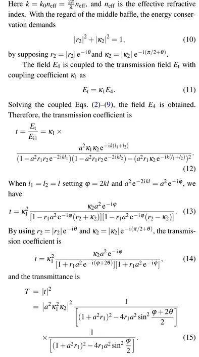
Firstly, a F-P cavity in MIM waveguide is studied. The MIM waveguide width is 60 nm, in which two baffles with space oflare inserted to form a cavity,as shown in Fig.1(a).A plane wave with electrical fieldEyis incident from the input port, and the waves propagate along the waveguide and interact with the cavity. The transmission in the output port is obtained. The finite difference time domain (FDTD) method coded by ourselves is used to simulate the interactions between electric fields and the structures. Mesh cell size is Δx= Δy= 1 nm. In FDTD simulation, the permittivity of silver varies with incident wave frequency according to the Drude model[32,33]
Hereε∞=3.7 is the permittivity constant,ωp=9.1 eV is the plasma resonant frequency andγ=0.018 eV is the loss constant.
Thex-ysection view for the single cavity is shown in Fig. 1(b). The thickness of metal bafflesd=15 nm and the space between theml=964 nm. The transmission spectrum is obtained through the FDTD method,as shown in Fig.1(c).There exists a peak atλ=1405.2 nm. The module distribution of electrical fieldEycorresponding to the peak is shown in Fig. 1(d). Obviously, two standing waves appear in the cavity,which demonstrates that second-order resonance leads to the transmission peak. The phase distribution is shown in Fig.1(e). There is an initial phase difference Δφ=πbetween the left and right fields.
Then a two-cavity structure is considered, which is formed by inserting a baffle with thickness of 15 nm in the middle of the cavity, as shown in Fig. 2(a). Electromagnetic waves can transmit through the middle baffle or be reflected.So the resonances in two cavities couple to each other and the coupled cavity (CC) forms. The transmission spectrum is shown in Fig.2(b). There exist two peaks,the opposite coupled mode(OCM)atλOCM=1405.2 nm and the positive coupled mode (PCM) atλPCM=1550.5 nm in the transmission spectrum, respectively. The module distributions of electrical fieldsEycorresponding to the OCM and PCM peaks are shown in Figs.2(c)and 2(d),respectively. Obviously,a standing wave appears in each cavity both atλOCM=1405.2 nm andλPCM=1550.5 nm. The couplings of the first-order resonances in each cavity lead to the two peaks. For the phase distribution atλOCM=1405.2 nm shown in Fig.2(e),there is a phase difference close toπbetween the left and right cavities. For the PCM peak at 1550.5 nm,the fields have the same phase in two cavities,as shown in Fig.2(f).
The thickness of the middle baffles has influence on the coupling resonances, as shown in Figs. 3(a)-3(e). As the thickness of middle baffle equals to 3 nm, the PCM peak appears at 2049.0 nm and the OCM peak appears at 1405.2 nm in Fig.3(a). The wavelength variances of two peaks with the baffle thickness are shown in Figs.3(a)-3(e). With the middle becoming thick, the PCM peak blue shifts. Whent=50 nm,the PCM peak almost meets with the OCM peak. One can see that the PCM blue shifts and the OCM remains almost unchanged with the thickness increasing,that is,the resonant mode in the CC splits when the middle baffle becomes thin.
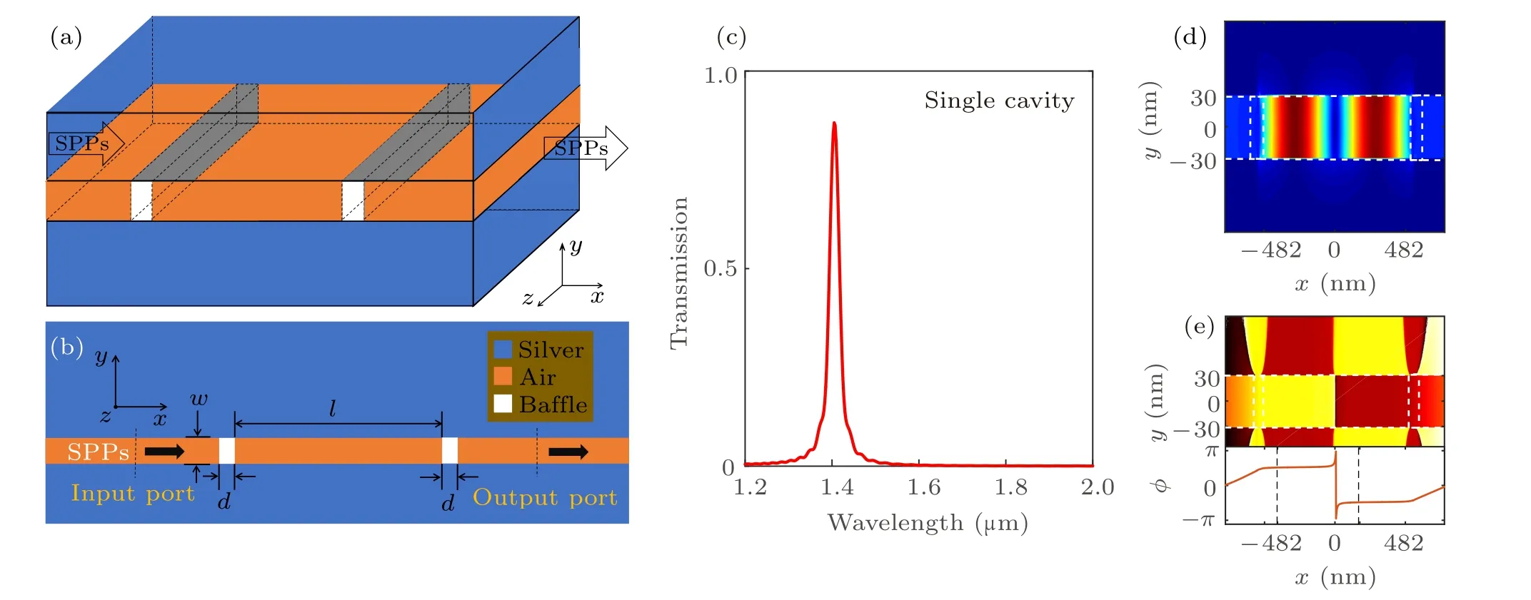
Fig.1. A cavity in MIM waveguide. (a)Schematic diagram,(b)the x-y section view of the structure. (c)Transmission spectrum. The distributions of(d)module and(e)phase of the electrical field at λ =1405.2 nm.

Fig.2. The properties of CC in MIM waveguide. (a)Schematic diagram. (b)Transmission spectrum. The module distributions of electrical fields at(c)λOCM=1405.2 nm and(d)λPCM=1550.5 nm. The phase distributions at(e)λOCM=1405.2 nm and(f)λPCM=1550.5 nm. (g)Opposite coupling and(h)positive coupling between two cavities.
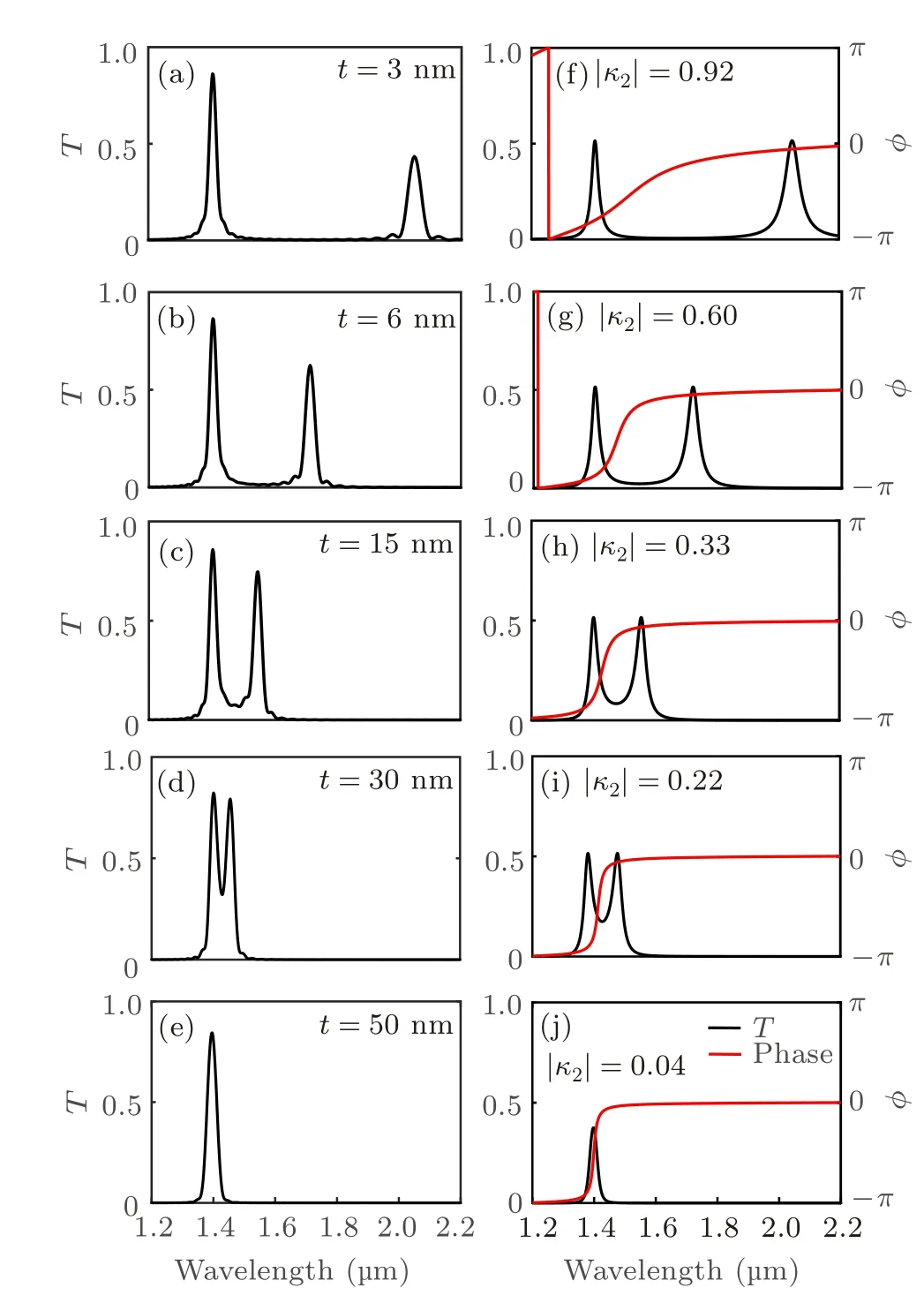
Fig.3. Influences of baffle thickness or coupling strength on transmission. (a)-(e)The FDTD simulation transmission spectra,(a)t =3 nm,(b)t =6 nm,(c)t =15 nm, (d)t =30 nm, (e)t =50 nm. (f)-(j)The transmission spectra T with different coupling coefficients calculated by Eq.(15)and the phases by Eq.(18)based on the CMT.
When the baffle thicknesstvaries from 3 nm to 50 nm,the wavelength of PCM changes about 644 nm, showing a large wavelength-modulation range. The wavelength modulation without optical path change is quite different from classical cavity length or refractive index tuning.The property can be used to design a new tunable laser cavity for SPP integration.
3. Coupled mode theory analysis
The coupled-mode theory (CMT)[34]is used to analyze the optical process in the structure for coupled mechanism and resonance condition,as shown in Fig.4.
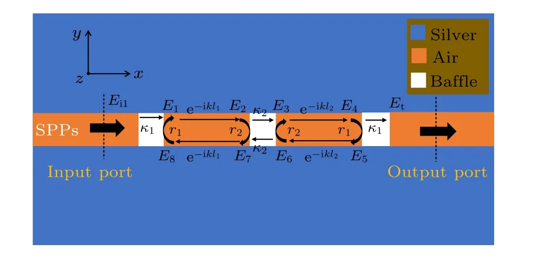
Fig.4. The coupled process in CCs.
The incident fieldEi1is coupled to theE1in the left cavity with couple coefficientκ1. ThenE1propagates toE2,E2is reflected toE7with reflection coefficientr2by the middle baffle andE2transmits through the middle baffle toE3with coupling coefficientκ2. On the one hand,one traveling round in the left cavity forms:E7propagating toE8,E8being reflected toE1with reflection coefficientr1,andE1propagating toE2.On the other hand,the other traveling round in the right cavity forms:E3propagating toE4,E4being reflected toE5with reflection coefficientr1,andE5propagating toE6. In the middle baffle,E6is reflected toE3with reflection coefficientr2and transmits toE7with coupling coefficientκ2. The transmitted fields join the traveling round in the left cavity. The coupled equations are given as

Transmittance gets the maximum when the coupled resonances happen. According to Eq.(15),the coupled resonance condition is

By using Eq.(15), the transmission spectra for different coupling coefficients are calculated, as shown by black lines in Figs. 3(f)-3(j). Hereneff=1.45,r1=-0.91,a=0.99, andκ1=0.415i. One can see that the long-wavelength peak blue shifts and the short-wavelength peak remains unchanged with the coupling coefficient|κ2| decreasing. The resonant mode splits when the coupling becomes strong. The coupling becomes weak due to the thickness increase of the middle baffle. Therefore,the thickness increasing of the middle baffle in FDTD corresponds to the coupling coefficient|κ2|decreasing in Eq. (15) of the CMT results. Comparing the FDTD simulations with the CMT analysis, one can see that the mode splitting in the FDTD simulation coincides well with that of the CMT analytical results when the middle baffle becomes thin or the coupling strength becomes weak.
In single F-P cavity,the fieldr1Ereflected by one end interferes with a fieldr1Ereflected by the other end,leading to a resonance formulaEcavity=E0/[1-r2exp(-i2kL)]. By contrasting the denominator of Eq.(13)to that of single F-P cavity resonance,it is found that the formula 1-r1a2e-iφ(r2+κ2)in the denominator of Eq.(13)indicates the interference between the fieldr1Ereflected by the ends and the field (r2+κ2)Ecoming from the middle baffle in the CCs. When the phase condition in Eq. (16) is satisfied, the oscillation builds up and the resonance happens, producing positive coupled resonance. In the same way, the formula 1-r1a2e-iφ(r2-κ2)in Eq. (13) indicates the fieldr1Ereflected by the ends and the field(r2-κ2)Ecoming from the middle baffle interfere in the CCs. When the condition in Eq. (17) is satisfied, the oscillation builds up and resonance happens,producing opposite coupled resonance.
According to Eqs. (16) and (17), the phases introduced by the opposite and positive couplings are different. In the positive coupling,the introduced phase by coupling is 2θwithθ=sin-1|κ2|. While there is no phase introduced in the opposite coupling. The resonant conditions for the opposite and positive couplings are different. This leads to resonance mode splitting. When the|κ2| increases from 0 to 1 (that is,θincreases from 0 toπ/2),the resonance mode splits into the opposite and positive coupled resonance modes. The splitting distance is 2θ=2sin-1|κ2|.
The phase difference betweenE1andE3is considered.By using Eqs.(5)-(9),the electrical field ratio is obtained as
The argument of ratioPrepresents the phase difference betweenE1andE3. The phase differences for different coupling strengths are calculated through Eq. (18), as shown by the red lines in Figs. 3(f)-3(j). One can see, there is nearlyπ’s initial phase difference betweenE1andE3for the shortwavelength mode. While the phase difference is nearly zero for the long-wavelength mode. Similarly, in FDTD result,there is nearlyπ’s initial phase difference between two cavities atλ=1405.2 nm[in Fig.2(e)]. Forλ=1550.5 nm,there are the same phases in two cavities [in Fig. 2(f)]. Therefore,the CMT results coincide with the FDTD results.
Based on the CMT and FDTD results, it is believed that the transmissions through the cavity arise from the coupled resonances between the states|φ1〉in left cavity and|φ2〉in right cavity. The opposite coupling of|φ1〉and|φ2〉leads to the short-wavelength peak atλ=1405.2 nm. The opposite coupling is schemed in Fig.2(g)and the coupling state is

There are the same phases in two cavities. The positive coupling resonant mode forms when the condition in Eq. (16) is satisfied.
4. Resonances in multiple-cavity structures
The coupled resonances in three- and four-cavity structures are considered. The three-cavity structure is shown in Fig. 5(a). When the length of every cavityl1=l2=l3=472 nm and the thickness of bafflet= 15 nm, the transmission spectrum is obtained, as shown in Fig. 5(b). Three peaks appear atλM1= 1370.7 nm,λM2= 1469.3 nm andλM3=1564.0 nm. The field module and phase distributions corresponding to the three peaks are shown in Figs. 5(c)-(e)and(f)-(h), respectively. ForλM1=1370.7 nm, the standing wave appears in each cavity. The phase difference Δφ1,2=πand Δφ1,3=0. Here Δφi,jrepresents the initial phase difference between cavityiand cavityj. ForλM2=1469.3 nm,the standing waves appear cavity 1 and cavity 3,and the phase difference Δφ1,3=π. ForλM3=1564.0 nm, the standing wave appears in each cavity and the phases are the same in three cavities.
The thickness of the middle baffles has influences on the transmission spectra [in Fig. 5(i)] and the wavelengths of the three peaks[in Fig.5(j)].With the thickness of the middle baffles increasing, the peaks M2 and M3 blue shift, while peak M1 remains invariant, as shown in Figs. 5(i)-5(j). Based on the two-cavity coupled resonance analysis, it is believed that the transmission peaks originate the coupled resonances of the state|φ1〉in cavity 1, the state|φ2〉in cavity 2 and the state|φ3〉in cavity 3. Three coupling mechanisms are given in Figs.5(k)-5(m). The opposite coupling of the states|φ1〉,|φ2〉and|φ3〉is schemed in Fig.5(k)and is expressed as

where eiπrepresents the initial phase difference between|φ2〉and|φ1〉.By combining with the phase distribution in Fig.5(f),it is believed the opposite coupling of the states|φ1〉,|φ2〉and|φ3〉contributes to the peak atλM1=1370.7 nm.
The opposite coupling between the state|φ1〉in cavity 1 and|φ3〉in cavity 3 schemes in Fig. 5(l). The opposite coupling is given as

There isπ’s initial phase difference between|φ1〉and|φ3〉. By combining with the phase distribution in Fig. 5(g), it is believed the opposite coupling between the states|φ1〉and|φ3〉contributes to the peak atλM2= 1469.3 nm. There isπ’s phase difference between cavity 1 and cavity 3, which leads to the destructive interference in cavity 2. Therefore, there is no standing wave appearing in cavity 2,as shown in Fig.5(d).
The positive coupling of the states|φ1〉,|φ2〉and|φ3〉is schemed in Fig.5(m)and the coupling is represented as

There are the same phases in the three cavities. By combining with the phase distribution in Fig.5(h),it is believed the positive coupling of the states|φ1〉,|φ2〉and|φ3〉contributes to the peak atλM3=1564.0 nm.
The four-cavity structure is shown in Fig.6(a). When the length of each cavityl1=l2=l3=l4=472 nm and the thickness of all bafflet=15 nm, the transmission is obtained, as shown in Fig. 6(b). Four peaks appear atλM1=1358.3 nm,λM2=1425.1 nm,λM3=1513.9 nm andλM4=1574.9 nm,respectively. The field module distributions corresponding to the four peaks are shown in Figs.6(c)-6(f),respectively.There are standing waves in all cavities at four resonant wavelengths.And the phase distributions corresponding to the four peaks are also shown in Figs.6(g)-6(j),respectively. For the peak atλM1=1358.3 nm,the phase difference Δφ1,2=Δφ1,4=πand Δφ1,3=0.
Fig.5. Couplings of three-cavity in MIM waveguide. (a)Schematic structure. (b)The transmission spectrum. The electrical field module distributions at(c)λM1 =1370.7 nm, (d)λM2 =1469.3 nm and(e)λM3 =1564.0 nm. The phase distributions at(f)λM1 =1370.7 nm, (g)λM2 =1469.3 nm and(h)λM3=1564.0 nm. (i)The transmission spectra of different baffle thicknesses. (j)The wavelengths of three peaks vary with the baffle thickness. The coupling mechanisms for three modes in the three-cavity structure,(k)the peak at λM1=1370.7 nm,(l)the peak at λM2=1469.3 nm and(m)the peak at λM3=1564.0 nm.
For the peak atλM2= 1425.1 nm, the phase differences Δφ1,2= Δφ1,3=πand Δφ1,4=π. For the peak atλM3=1513.9 nm,the phase differences Δφ1,2=0 and Δφ1,3=Δφ1,4=π. For the peak atλM4=1574.9 nm,the phase differences Δφ1,2=Δφ1,3=Δφ1,4=0.
The resonant modes in four-cavity structure originate the couplings of the state|φ1〉in cavity 1,the state|φ2〉in cavity 2,the state|φ3〉in cavity 3 and the state|φ4〉in cavity 4. Based on the field phase distributions in Figs. 6(g)-6(j) at the peak wavelengths,four coupling mechanisms are presented.
The first coupling schemes in Fig. 6(k). The coupling state is expressed as

where eiπrepresents that there isπ’s initial phase difference Δφ1,2=Δφ1,3=π. By combining with the phase distribution in Fig. 6(h), it is believed the second coupling resonance depicted in Eq.(25)contributes to the peak atλM2=1425.1 nm.
The third coupling mechanism is schemed in Fig. 6(m)and the coupling state is
There are the same phases in four cavities. By combining with the phase distribution in Fig.6(j), it is believed the coupling in Eq.(27)contributes to the peak atλM4=1574.9 nm.

Fig. 6. Couplings of four-cavity structure in MIM waveguide. (a) Schematic structure. (b) The transmission spectrum. The electrical field module distributions at (c) λM1 =1358.3 nm, (d) λM2 =1425.1 nm, (e) λM3 =1513.9 nm and (f) λM4 =1574.9 nm. The phase distributions at (g) λM1 =1358.3 nm,(h)λM2 =1425.1 nm,(i)λM3 =1513.9 nm and(j)λM4 =1574.9 nm. The coupling mechanisms for four peaks,(k)mode 1,(l)mode 2,(m)mode 3 and(n)mode 4.
5. Wavelength management devices designing
A device composed of multiple cavities is designed to manage the SPPs propagation,as shown in Fig.7(a).The SPPs propagating in the main waveguide are routed to 4 channels via different CCs in waveguides. The spectra transmission from channel 1 with only one cavity is shown in Fig.7(b).When the length of the cavitylc1=474 nm,only one signal is taken out through the single-cavity resonance. The signal wavelength varies from 1350 nm to 1743 nm when the cavity lengthlc1changes from 424 nm to 574 nm. When two coupled cavities are designed in channel 2, two-channel signals are taken out from channel 2,as shown in Fig.7(c). When the cavity length decreases from 474 nm to 434 nm,the wavelengths of two signals display a blue shift. When the ratio of two cavity lengths changes, the OCM blue shift while PCM red shift, as shown in Fig.7(d). The resonant wavelengths of the two modes can be tuned through the cavity length and baffle thickness. When the baffle thickness varies,only the PCM wavelength changes.While the cavity length varies,both the PCM and OCM wavelengths change.
In channel 3, three cavities are aligned in MIM waveguide,and three-channel signals are taken out through coupled resonance modes, as shown in Fig. 7(e). The wavelengths of three signals vary with the cavity length. To take out 4 signals,four cavities are designed in MIM waveguide.The output from channel 4 is shown in Fig. 7(f). One can see the channel number can be controlled through cavity number and the wavelengths can be controlled through the baffle thickness and cavity length. The flexible multiple wavelength SPPs routing is realized.
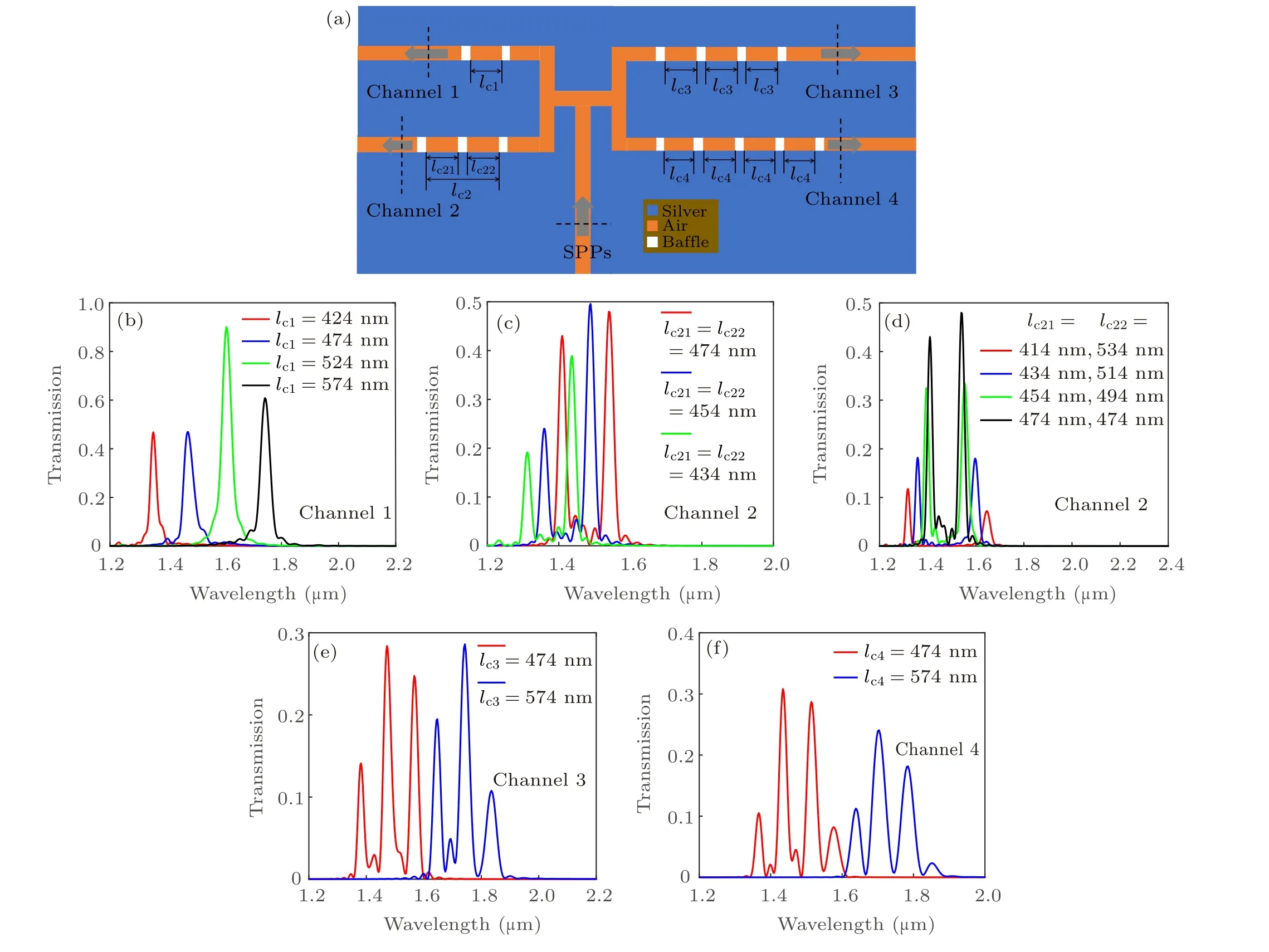
Fig.7. Multiple wavelength routing through the CCs. (a)Schematic structure. (b)The output from channel 1. The output from channel 2 through two CCs(c)with the same cavity lengths and(d)with different cavity lengths. (e)The output from channel 3. (f)The output from channel 4.
6. Conclusion
Nanoscale CC resonances in MIM waveguide have been investigated. It is found that the couplings of the first resonant modes in each cavity lead to new resonant modes with different wavelengths. The resonance wavelengths can be tuned through the coupling strength. The coupling mechanisms of these resonance modes are analyzed and the resonant conditions are obtained through the coupled-mode theory. Based on the results, a wavelength-management device is designed to realize the multiple-wavelength SPPs routing. The single cavity, two-cavity, three-cavity and four-cavity structures can route different channel numbers with different wavelengths to outputs. This can be used to design multiple-wavelength resonance cavities for laser and filters in SPPs integrated circuits,stimulated Raman and Brillouin scattering enhancements in nonlinear optics.
Acknowledgment
Project supported by the National Natural Science Foundation of China(Grant No. 11764006).
杂志排行

Chinese Physics B的其它文章
- Superconductivity in octagraphene
- Soliton molecules and asymmetric solitons of the extended Lax equation via velocity resonance
- Theoretical study of(e,2e)triple differential cross sections of pyrimidine and tetrahydrofurfuryl alcohol molecules using multi-center distorted-wave method
- Protection of entanglement between two V-atoms in a multi-cavity coupling system
- Semi-quantum private comparison protocol of size relation with d-dimensional GHZ states
- Probing the magnetization switching with in-plane magnetic anisotropy through field-modified magnetoresistance measurement