A 3D SiC MOSFET with poly-silicon/SiC heterojunction diode
2022-01-23ShengLongRan冉胜龙ZhiYongHuang黄智勇ShengDongHu胡盛东HanYang杨晗JieJiang江洁andDuZhou周读
Sheng-Long Ran(冉胜龙), Zhi-Yong Huang(黄智勇), Sheng-Dong Hu(胡盛东),Han Yang(杨晗), Jie Jiang(江洁), and Du Zhou(周读)
Chongqing Engineering Laboratory of High Performance Integrated Circuits,School of Microelectronics and Communication Engineering,Chongqing University,Chongqing 400044,China
Keywords: heterojunction diode,SiC MOSFET,switching loss,on-state resistance
1. Introduction
Owing to its representative wide band-gap material and device performance, SiC metal-oxide-semiconductor fieldeffect transistor (MOSFET) is widely used in the power systems on account of the properties of low on-state resistance, high power density, outstanding switching characteristics,etc.[1-3]To obtain a high efficiency and a low power loss,it is important to increase the reliability of the SiC MOSFET and reduce the chip size. When the conventional SiC trench MOSFET (C-TMOS) is used in the power systems, a Schottky barrier diode (SBD) must be paralleled to prevent the aged deterioration,[4-7]which may result in high cost,extra power loss,and undesirable stray inductances. Several optimized structures such as the SiC trench MOSFET with a merged SBD have been studied, aiming at reducing the chip cost, enhancing the reverse recovery characteristics, and reducing the power loss,[8-12]etc. Additional fabrication and photolithography process are the main difficulties in commercializing these structures. The reliability of the gate oxide layer is also a major concern for the SiC MOSFET.Inserting a highly-doped P+ layer at the bottom of the trench gate oxide proves to be an effective method to improve the gate oxide reliability.
Heterojunction diode consisting of poly-silicon and SiC has a crucial influence on the reverse recovery time.[13,14]In this paper, a three-dimensional (3D) SiC MOSFET with an HJD embedded on one side of the gate oxide is presented and analyzed,which offers a new method to reduce the power loss and improve the electric characteristics for the SiC MOSFET.
2. Device structure and mechanism
Figures 1(a) and 1(b) show the device structures of the C-TMOS and the 3D HJD-TMOS, respectively. Compared with the conventional TMOS,the 3D HJD-TMOS has an HJD structure consisting of the poly-silicon/SiC, and the HJD is embedded in thezaxis,which is an improvement based on the two-dimensional(2D)device.[15]Figure 1(c)shows the crosssection view and figure 1(d) shows the energy band diagram along the poly-silicon layer and the current spreading layer(CSL).
The valence band and conduction band for the HJD are 1.73 eV and 0.45 eV,respectively. The electron barrier heightΦBN(about 1.48 eV)is determined by the Fermi-levelEfand the conduction bandEC. This barrier height can cause a small forward voltage(VF)when the device is forwardly biased. On the contrary,it can cause a high breakdown voltage(BV)when the device is reversely biased. And the barrier height ΔECwill control the parasitic diode in turn on state,creating a large onvoltage(VPN). Furthermore,a highly-doped P+layer is introduced into the structure encircling the gate oxide on the same side as the HJD and under the gate oxide to improve the gate oxide reliability.[16-18]It can lighten the electric field concentration around the regions near to the gate oxide and HJD,as well as reduce the overlapping between the gate layer region and the drift layer,realizing a highBVand a quick switching time.
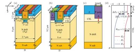
Fig.1. Structure diagrams of(a)C-TMOS,(b)HJD-TMOS,(c)y-z cross-section view(x=0),and(d)energy band among line AA′ for HJD-TMOS.
In this work, the P-poly and the P+ shielding layer extend along the wholezdirection. In order to make a fair comparison,the two devices have the same major dimensions and doping concentrations. To get aBVabove 650 V, the thickness and doping concentration for the channel layer are set to be 0.8µm and 3×1017cm-3, respectively. The doping concentration of the drift layer(Nd)is 7.5×1015cm-3. The thickness of epitaxial layer from the N-substrate to the top surface of the device is 9.2µm. The width(Wtrench)and the depth for the trench gate are set to be 0.7µm and 1.2µm,respectively.The thickness of the gate oxide on the side and at the bottom are 60 nm and 120 nm, respectively. To simulate the device tape-out process,the traps are set with a doping concentration of 5×10¹²eV-1·cm-2, which is located at the interface between SiO2and SiC. The CSL doping concentration is set to be 2×1016cm-3. The thickness of the CSL in HJD-TMOS set to be 0.8 µm, and in the C-TMOS has been optimized to obtain the same on-state resistance(Ron).
The Sentaurus TCAD tool is used to analyze the physical mechanisms for the SiC devices. The Shockley-Read-Hall(SRH), Auger, and Okuto-Crowell models are chosen in the recombination process. The mobility model contains incomplete ionization, high-field saturation, enormal, and dopingdependence.
3. Results and discussion
The key device parameters for the 3D HJD-TMOS are the width of the P-type poly-silicon(LP-poly)and the distance between the poly-silicon trench and the gate trench(LP). Figure 2 shows the influences of theLP-polyandLPon the electric field distributions and output performances for the HJDTMOS.
AsLP-polyincreases from 0.7 µm to 1.3 µm, the average electric field decreases slightly. While asLPincreases from 0.2 µm to 1.0 µm, the average electric field increases,which will significantly affect the breakdown voltage. Figure 2(b)shows that with a givenLP,the drain-source voltageVdsincreases with theLP-polyrising when theIdsreaches to 100 A/cm2, which means that a smaller on-resistance can be obtained with a shorterLP-poly.
Figure 3(a)shows the relation of theBVwithLPfor three different values ofLP-polyfor the HJD-TMOS. It is set that the device reaches to the breakdown point when the drainsource currentIdsrises to 10µA/cm2. TheBVincreases whenLPincreases from 0.2 µm to 1.0 µm with the sameLP-poly.However,theBVdecreases asLP-polyincreases from 0.7µm to 1.3 µm with the sameLP. The relations of theRonand the turn-on voltage of the body diode (VPN),VFwithLPandLP-polyare shown in Fig. 3(b). When the cell pitch size increases asLPandLP-polyincrease, theRonincreases as well.TheVFis almost a constant because it relates only to the HJD.TheVPNincreases with the decrease ofLPor the increase ofLP-poly,andVPNis 4.3 V with anLP-polyof 0.7µm and anLPof 1.0µm,which is still much larger than that of the conventional SiC pn junction (about 2.9 V). This indicates that the HJD-TMOS has a good control of the body diode in the turnon state. Figure 3(c)shows the variation ofRonwith the thickness of CSL in C-TMOS.With the increase of the thickness of CSL,theRonchanges in an opposite way.AnLPof 0.4µm and anLP-polyof 1.0µm are chosen to analyze the device’s performance for HJD-TMOS,and theRonis about 1.89 mΩ·cm2. In order to reach the sameRonlevel as the HJD-TMOS,the thickness of CSL in C-TMOS is set to be 0.36 µm, and anRonof 1.88 mΩ·cm2is obtained just as shown in Fig.3(c). The cell pitches of the two devices are 2.7µm and 3.1µm,respectively.
Figure 4(a) shows theI-Vcurves in the turn-off state for the two devices. The HJD-TMOS provides a higherBV.Figures 4(b)and 4(c)show thex-ycross-section electric field distributions atVds=650 V for the two devices. Owing to a widerLPand a larger P+ shielding region, the peaks of the high electric fields in the corners of the gate oxide and P+region are both smaller for the HJD-TMOS.
Figure 5 shows the electric field distributions in different cross-sections through the biggest electric field points for the two devices. It is obvious that in thex-zcross-section andx-ycross-section, the average electric fields are improved for the HJD-TMOS,which is the reason why the device has a largerBV.
Figure 6 shows theI-Vperformances for the two devices.Figure 6(a)displays theI-Vrelations in the turn-on state. The two devices have a similar on-state current except in the transition region because of the same level ofRon. From Fig.6(b)it can be seen that HJD-TMOS has a much lowerVFthan CTMOS,resulting in prominent reduction of the dead-time loss.As shown in Fig. 6(c), theVPNof the optimized HJD-TMOS increases to 4.6 V atIdsH=10 A/cm2,whileVPNis 2.9 V for the C-TMOS,which means that it can better control the body diode in the turn-on state.

Fig.2. (a1)-(a3)Vertical electric field distributions,(b1)-(b3)output I-V curves for some values of LP and LP-poly. Electric field distributions are chosen to be at their corresponding breakdown points.
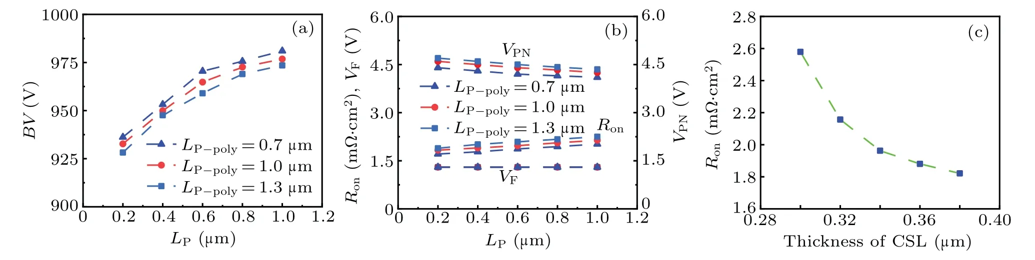
Fig. 3. (a) Curves of BV versus LP for different values of LP-poly; (b) curves of Ron,VPN, and VF for different values of LP-poly; (c) curve of Ron versus thickness of CSL in C-TMOS.
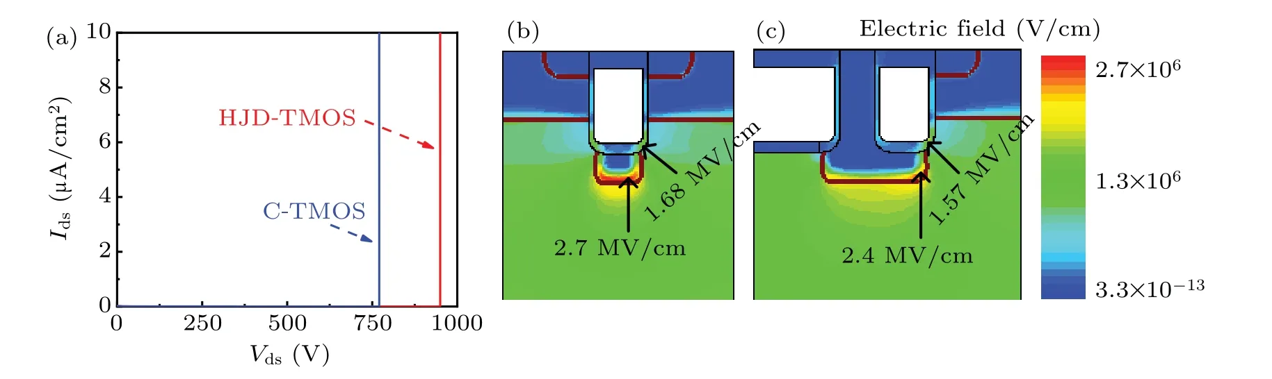
Fig.4. Electric characteristics in the turn-off state for the two devices: (a)I-V curves,(b)x-y cross-section electric field in C-TMOS,(c)x-y cross-section electric field in HJD-TMOS,with electric field distributions chosen at Vds=650 V.

Fig.5.Electric field distributions when breakdown occurs for two devices:(a)x-z cross-section electric field distributions,(b)x-y cross-section electric field distribution,with electric field distributions chosen at their corresponding breakdown points.

Fig. 6. Forward characteristics and reverse characteristics of two devices: (a) output curve (Vgs =15 V), (b)VF curves (Vgs =-5 V), and (c)VPN curve(Vgs=-5 V).
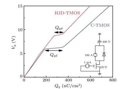
Fig.7. Relations of gate voltage with gate charge for two devices,with insert showing test circuit.
Figure 7 shows the relations of the gate voltage(Vg)with gate charge(Qg)for the two devices. Compared with the conventional device,the HJD-TMOS has a smaller miller plateau due to the smaller overlapping region between the gate layer region and the drift layer. The gate-drain charge (Qgd) decreases down to 83 nC/cm2,which is a 43.2%reduction from 150 nC/cm2of the C-TMOS. This indicates that the HJDTMOS has a remarkable reduction of power loss.
Figures 8(a)and 8(b)show the switching waveforms and switching test circuit for the C-TMOS and the HJD-TMOS.Although the C-TMOS is anti-paralleled to the SiC SBD,the current spike of the HJD-TMOS is smaller in the turn-on state.Figure 8(c)shows the contrastive results of the switching loss for the two devices. The switching loss of the HJD-TMOS is reduced by 48.6% in comparison with the conventional one.The introduced HJD structure and the lower charge are the main factors that give rise to the lower switching loss and lead to the other excellent device performances at the same time as summarized in Table 1.
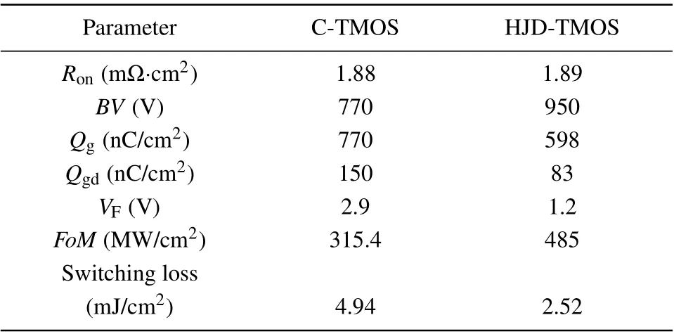
Table 1. Device parameters and characteristics.
Figure 9 shows the variations of figure of merit (FoM)with length of HJD trench for different values of drift doping concentration(Nd)for the HJD-TMOS.The values of the mentioned C-TMOS and HJD-TMOS are both listed. It indicates that withNdkept unchanged, theFoMincreases as the trench length increases to 1.6 µm, at which theFoMis the largest. TheFoMincreases as the drift doping concentration decreases. When the drift doping concentration decreases from 6×1015cm-3to 5.5×1015cm-3, theFoMincreases slightly. The channel near the HJD plays a minor role in the whole structure when the trench length increases or the drift doping concentration decrease to a limited extent. And compared with the simulated C-TMOS, each of all partial HJDTMOSs has its own betterFoM.the 3D SiC MOSFET,which has a great potential to be a great candidate in the power systems.

Fig.8. (a1)-(a2)Switching waveforms of two devices,(b)test circuit,and(c)switching loss.
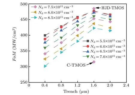
Fig.9. Curves of FoM versus length of HJD trench at different values of Nd for HJD-TMOS,with LP and LP-poly being 0.4µm and 1.0µm,respectively.
Acknowledgements
Project supported by the Natural Science Foundation Project of Chongqing Science and Technology Commission,China(Grant No.cstc2020jcyj-msxmX0243),the Fundamental Research Funds for the Central Universities,China(Grant No.2020CDJ-LHZZ-024),and the Chongqing Technology Innovation and Application Development Key Project, China(Grant No.cstc2019jscx-zdztzxX0051).
4. Conclusions
A 3D SiC trench MOSFET embedded with an HJD structure is presented in this work. The embedding of HJD can suppress the parasitic body diode. The high-doped P+shielding layer can reduce the strength of the electric field near the gate trench. The reverse recovery characteristic, the breakdown voltage and the switching property are all improved for
猜你喜欢
杂志排行

Chinese Physics B的其它文章
- Superconductivity in octagraphene
- Soliton molecules and asymmetric solitons of the extended Lax equation via velocity resonance
- Theoretical study of(e,2e)triple differential cross sections of pyrimidine and tetrahydrofurfuryl alcohol molecules using multi-center distorted-wave method
- Protection of entanglement between two V-atoms in a multi-cavity coupling system
- Semi-quantum private comparison protocol of size relation with d-dimensional GHZ states
- Probing the magnetization switching with in-plane magnetic anisotropy through field-modified magnetoresistance measurement