Heterogeneous integration of InP HEMTs on quartz wafer using BCB bonding technology
2022-01-23YanFuWang王彦富BoWang王博RuiZeFeng封瑞泽ZhiHangTong童志航TongLiu刘桐PengDing丁芃YongBoSu苏永波JingTaoZhou周静涛FengYang杨枫WuChangDing丁武昌andZhiJin金智
Yan-Fu Wang(王彦富) Bo Wang(王博) Rui-Ze Feng(封瑞泽) Zhi-Hang Tong(童志航)Tong Liu(刘桐) Peng Ding(丁芃) Yong-Bo Su(苏永波) Jing-Tao Zhou(周静涛)Feng Yang(杨枫) Wu-Chang Ding(丁武昌) and Zhi Jin(金智)
1University of Chinese Academic of Sciences,Beijing 100029,China
2High-Frequency High-Voltage Device and Integrated Circuits Center,Institute of Microelectronics,Chinese Academy of Sciences,Beijing 100029,China
3Guangxi Key Laboratory of Precision Navigation Technology and Application,Guilin University of Electronic Technology,Guilin 541004,China
Keywords: heterogeneous integration,InP high electron mobility transistor,quartz,small-signal model
1. Introduction
InP-based high electron mobility transistors(HEMTs)are considered as one of the most competitive semiconductor devices for millimeter and terahertz monolithic integrated circuits. These applications are based on the excellent properties of the InP-based HEMTs, such as low noise, low power consumption and high gain performance.[1-6]However,owing to the high dielectric constant of InP,the transmission loss of InP-based monolithic integrated circuits is large, and the application of InP-based HEMTs in the high-frequency field is restricted. Therefore,it is necessary to replace the substrate of InP HEMTs through heterogeneous integration.
In recent years, many structures and methods have been used to achieve the heterogeneous integration of InP-based transistors on Si and other substrates in order to gain better performance and larger application fields. Liuet al.[7]have reported the heterogeneous integration of InP-based heterojunction bipolar transistor (HBT) structures on Si substrates by using molecular beam epitaxy, which have the similar direct current (DC) and radio frequency (RF) performance to the device grown on lattice-matched InP substrate. Hayashiet al.[8]have investigated the layer transfer of GaAs,InP,GaSb,and InAs by using hydrogen ion exfoliation and wafer bonding. Kimet al.[9]have presented the InGaAs-on-insulator fabrication from an InGaAs layer grown on a Si donor wafer with a III-V buffer layer instead of growth on an InP donor wafer,and such transistors exhibit the high electron mobility and uniform distribution of the leakage current.
Quartz has the features of low dielectric constant and insulation, so it is very suitable to serving as the substrate for high frequency circuits. The excellent RF characteristics of InP-based HEMTs and the low dielectric constant of quartz wafer can be combined on the same device by using heterogeneous integration.The heterogeneous integration of InP-based transistors on quartz wafer shows a promising future,and the design, fabrication and characteristics of heterogeneous integration of InP HEMTs on quartz wafer still need further studying.
In the present research, we describe the design, fabrication, and characteristics of the heterogeneous integration of In0.52Al0.48As/In0.7Ga0.3As InP-based HEMTs on quartz wafer with 100-nm gate-length. The reverse-grown InP epitaxial structure is used to realize the layer transfer with the BCB bonding technology. The BCB bonding technology is chosen here in this work,for the BCB bonding is not sensitive to the surface morphology of the bonded wafer, the temperature during the bonding process is relatively low,and the BCB after bonding is robust again the attack from various strong acids, strong alkalis, and chemical solvents. A small signal equivalent circuit model is established to evaluate the mechanism of RF performance,and the excellent agreement between the measured and simulatedfT,fmax,andkis observed.
2. Experiment
Figure 1(a) shows the epitaxial structure of the HEMT used in this work and figure 1(b) shows a schematic crosssectional view of our heterogeneous integrated InP-based HEMT structure. All epitaxial layers were grown by molecular beam epitaxy (MBE) on a 3-inch (1 inch=2.54 cm)semi-insulating (100) InP substrate.[10,11]From bottom to top, the epitaxial layers constituting a 50-nm InP buffer were a 100-nm In0.53Ga0.47As etching stopper layer, a 10-nm InP etching stopper layer, a 40-nm Si-doped composite InGaAs cap layer, a 4-nm InP etching stopper layer, an 8-nm In0.53Al0.47As Schottky barrier layer,Si delta doping layer with 5×1012cm2doping concentration,a 3-nm In0.52Al0.48As spacer layer, a 10-nm In0.7Ga0.3As channel layer, and a 500-nm In0.52Al0.48As buffer. A 10-nm Si-doped In0.65Ga0.35As layer,a 15-nm Si-doped In0.53Ga0.47As,and a 15-nm Si-doped In0.53Al0.47As transition layer constituted the composite cap layer to facilitate the formation of non-alloyed Ohmic contacts. After device fabrication we could obtain the heterogeneous integration of InP HEMTs on quartz wafer as shown in Fig.1(b).
The device fabrication started with interconnections of InP epitaxy and quartz through BCB (3022-46, Dow Chemical) adhesive bonding and InP substrate removing as shown in Fig. 2. The epi-wafer and quartz were first treated in oxygen plasma,and then placed on a hot plate to remove surface moisture. After that, the wafers were coated with BCB, precured for 10 min and finally placed in an oven filled with N2at 0.18 MPa pressure for curing BCB.
Then the origin InP substrate and InP buffer were removed by using HCl:H2O =3:1, the InGaAs stopper layer was removed by using H3PO4:H2O2:H2O=3:1:50 and the InP etched stopper layer was removed by using HCI:H3PO4=1:4 to expose the InGaAs cap layer. After mesa-etching, Ohmiccontact formation,and T-shaped gate recess via e-beam lithography, the heterogeneous integration of InP HEMTs on a quartz wafer was fabricated.
Detailed fabrication processes of the HEMT devices are similar to those of our previously reported devices.[12]And the process of heterogeneous integration is compatible with the process of CPWG MMIC.The specific contact resistivity was determined by transmission line method (TLM) to be about 1.09×10⁻⁷Ω·cm-2.
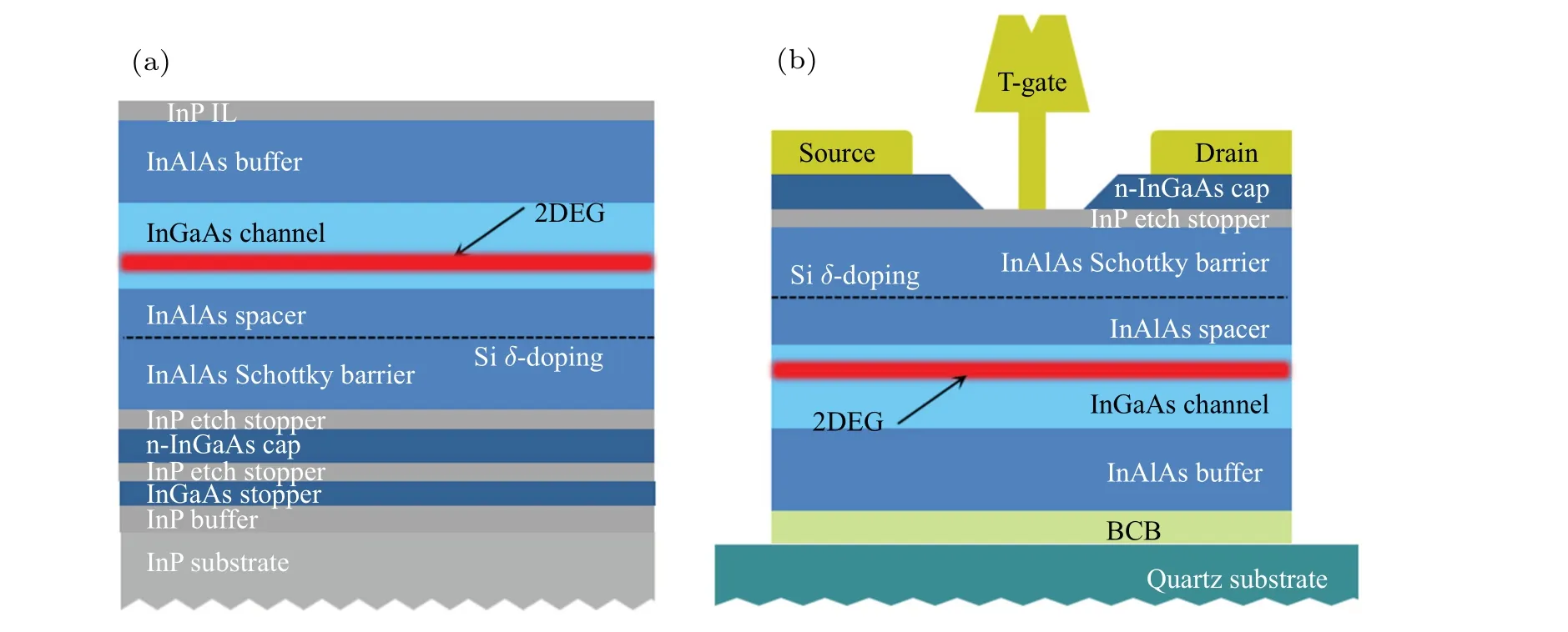
Fig.1. (a)Schematic cross-sectional view of epitaxial structure and(b)heterogeneous integrated InP-based HEMTs.
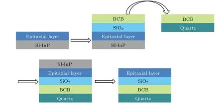
Fig.2. Process of BCB adhesive bonding and InP substrate removing.
To characterize the device performance,DC performance was revealed through HP4142 semiconductor parameter analyzer at room temperature,and the RF performance was characterized via an Agilent E8363B PNA vector network analyzer from 0.1 GHz to 50 GHz at room temperature. After measurement theS-parameters were extracted and studied.
3. Results and discussion
3.1. DC characteristics
Figure 3(a) shows the current-voltage (I-V) characteristics of a 100-nm gate length HEMT with a gate width of 2×20 µm at room temperature. The gate-source voltage(VGS) increases from-1.3 V to 0 V in steps of +0.1 V, and the drain-source voltage (VDS) is scanned from 0 V to 0.8 V.The heterogeneous integration of InP HEMTs on quartz wafer has good pinch-off characteristics,and we obtain a maximum drain current of 536.5 mA/mm which is achieved atVGS=0 V andVDS=0.8 V.The extrinsic transconductance(gm)and the drain current of the HEMT at a bias ofVDS=0.8 V are shown in Fig. 3(b). In addition, figure 3(c) shows the dependence ofgmon theVGSfor different values ofVDS. The device shows a pinch-off voltage of about-0.9 V. A maximum extrinsic transconductancegm,maxof 855.5 mS/mm is achieved atVGS=-0.6 V andVDS=0.8 V.Figure 3(d)shows the curve of gate leakage current of the HEMTsversus VGSforVDS=0 V in a range from-1.3 V to 0 V.The gate leakage current of the device is small enough for the LNA applications.
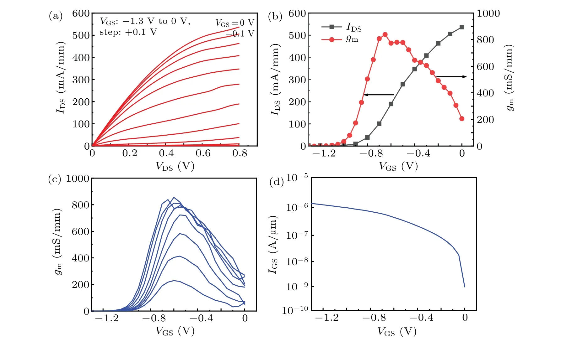
Fig.3. DC performances of heterogeneous integration of InP HEMTs with Lg of 100 nm,shown by(a)IDS-VDS curve of InP-based HEMTs,(b)transfer curves of InP-based HEMTs measured at VDS =0.8 V,(c)dependence of transconductance on VGS and VDS,and(d)gate leakage current versus VGS with VDS=0 V of HEMTs.
3.2. RF characteristics
The device under test is measured by using on-wafer open and short patterns to subtract pad capacitances and inductances from the measured deviceSparameters. Figure 4 shows the RF characteristics of heterogeneous integration of InP HEMTs withLgof 100 nm, which is approximately biased at a peakgmpoint ofVGS=-0.6 V andVDS=0.8 V.The current gainH21and the maximum stable gain(MSG)/maximum available gain (MAG) of the HEMTs are determined by the measuredS-parameter. Because of the limit of measuring frequency,we have to extrapolate the current gain (H21) and the maximum available power gain(MAG)by using a least-squares fitting with a-20-dB/decade slope after the parasitic parameters have been de-embedded to acquire thefTandfmax.[13]The value offTextrapolated fromH21is 262 GHz, andfmaxextrapolated from MAG is 288 GHz. However,the device is still unstable(k<1)at the maximum test frequency of 50 GHz,so it can be inferred that the actualfmaxcan be larger. ThefTandfmaxare expressed as follows:
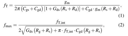
whereCgsis the parasitic capacitance from gate to source,Cgdis the parasitic capacitance from gate to drain,andRg,Rd,andRsare the parasitic resistances of gate, drain, and source, respectively. Thegmis the transconductance,theGdsis conductance between the drain and the source,andfT,intis the value offTfor the core part of HEMTs without any parasitic resistances and capacitances. Equations (1) and (2) show thatfTandfmaxhave a positive correlation withgm, and thefTandfmaxwill be good because of the highgm.
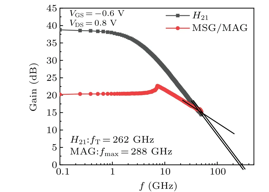
Fig.4. RF characteristics of heterogeneous integration of InP HEMTs with Lg of 100 nm.
In order to characterize the properties and performance of device,a small signal equivalent circuit model of heterogeneous integration of InP HEMTs on quartz wafer is built. Figure 5 illustrates a small signal equivalent circuit model for the devices,biased atVDS=0.8 V andVGS=-0.6 V.For the short gate length, the drain-source voltage will cause the sourceside barrier to drop,resulting in the drain-induced barrier lowering effect(DIBL),which affects the channel current characteristics. Therefore,τdsis added into the model to characterize the influence of drain-source voltage on channel current.[14,15]
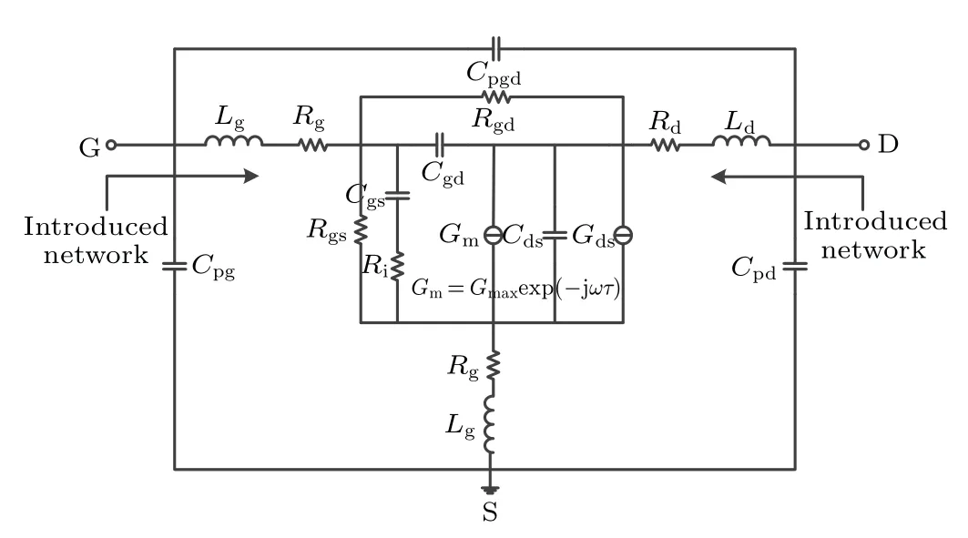
Fig.5. Small signal equivalent circuit model of heterogeneous integration of InP HEMTs on quartz wafer.
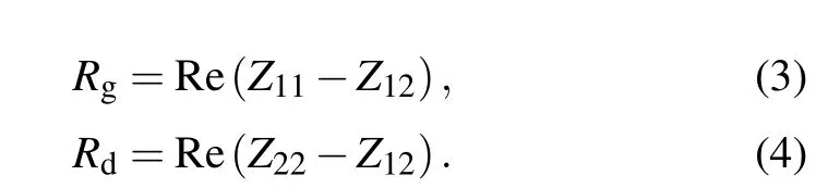
The extrinsic parameters contain parasitic capacitances,parasitic inductances, and parasitic resistances. We calculate the parasitic capacitances and parasitic inductances through theSparameters of the open structure and the short structure.Then we extracteRsby the YANG-LONG method and extracteRgandRdby the cold-FET method, and their expressions are as follows:
After all parasitic parameters are extracted, the intrinsic parameters are extracted.First,we obtain theSparameters of the intrinsic part of the device by using open-short de-embedding technology. Then according to the equivalent circuit structure of the intrinsic part,the intrinsic parameters are extracted through theYparameters as shown below:
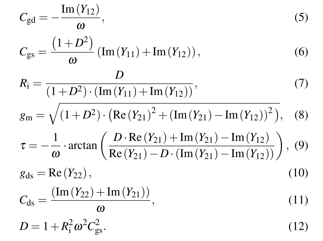
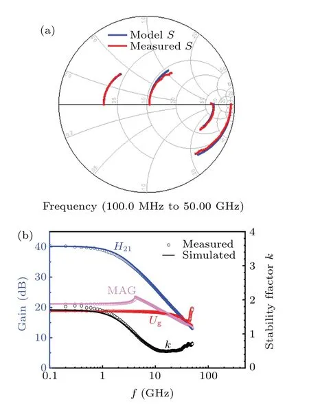
Fig.6. Fitting result of(a)S parameters and(b)RF performances.
Finally, we obtain all the values of the parameters in our model. And then the small signal equivalent circuit model topology of heterogeneous integration of InP HEMTs on quartz wafer is built in the Agilent’s advanced design system software(ADS),and the results are shown in Fig.5. After that, the topology is simulated and all values of parasitic parameters and intrinsic parameters are tuned to fit the model in ADS. The fitting result ofSparameters for the model is demonstrated in Fig.6. The parameters of small signal equivalent circuit of the device are given in Table 1. As we can see,the curved portion in the low frequency region ofSparameters and high frequency region ofSparameters can be fitted by the small signal equivalent circuit model,and the fitting results ofH21,MAG,andUgand stability factorkare all excellent.
A summary of RF characteristics of InP-based HEMTs with the same gate lengths and channel but different substrates is given in Table 2. We can see that the value offTof this work is relatively high in Table 2 though ourVDSis smallest(just 0.8 V). If we increase the maximumVDSof the device,thefTwill be higher and the RF performance of device will be better. The values offTandfmaxof these devices are all outstanding,which means that the heterogeneous integrations of InP HEMTs on other substrates have a promising future because the heterogeneous integrated device can take the full advantages of various materials and structures.

Table 1. Parameters of small signal equivalent circuit of device biased at fT,max.
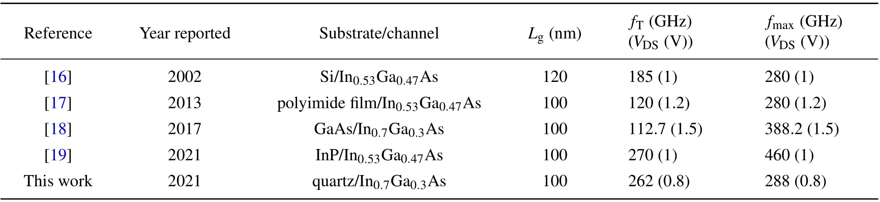
Table 2. Comparison aong published InP HEMTs on different substrates with gate length of 100 nm.
In Ref. [20], the aging of InP HEMT is influenced by a diffusion mechanism, the diffused impurities from gate electrode will reduce the carrier concentration in the epitaxial layer and cause device to age. Aging occurs in the gate area,so the change of the substrate has no effect on the aging caused by diffusion mechanism. As the thermal conductivity of quartz is much smaller than that of InP,the heat generated in the working process of the device will accumulate in the device and accelerate the aging of the device. In order to reduce this effect,MMIC structure with via holes and backside metal,such as CPWG,will be used to assist in heat dissipation.
4. Conclusions
In this work,the InP epitaxies grown in reverse order are used for heterogeneous integration with quartz wafers. The In0.52Al0.48As/In0.7Ga0.3As HEMTs with 100-nm gate length and 2µm×20µm gate width on quartz substrates are successfully fabricated after BCB bonding. The HEMTs exhibit good DC and RF performances, each with a maximum drain current of 536.5 mA/mm,a maximum extrinsic transconductancegm,maxof 855.5 mS/mm,a cut-off frequency of 262 GHz,and a maximum oscillation frequency of 288 GHz. In the end,the small signal equivalent circuit model is built to characterize the device performance;the fitting results ofSparameters and the fitting results of RF performances are good. The excellent results of the heterogeneous integration of InP HEMTs show promising high frequency applications.
Acknowledgements
Project supported by the National Natural Science Foundation of China (Grant No. 61434006). The authors would like to thank Li Yan-Kui for his assistance during the measurements. We are also grateful to all the members of High-Frequency High-Voltage Device and Integrated Circuits Center for their valuable help during the experiment.
猜你喜欢
杂志排行

Chinese Physics B的其它文章
- Superconductivity in octagraphene
- Soliton molecules and asymmetric solitons of the extended Lax equation via velocity resonance
- Theoretical study of(e,2e)triple differential cross sections of pyrimidine and tetrahydrofurfuryl alcohol molecules using multi-center distorted-wave method
- Protection of entanglement between two V-atoms in a multi-cavity coupling system
- Semi-quantum private comparison protocol of size relation with d-dimensional GHZ states
- Probing the magnetization switching with in-plane magnetic anisotropy through field-modified magnetoresistance measurement