Sensitivity of heavy-ion-induced single event burnout in SiC MOSFET
2022-01-23HongZhang张鸿HongXiaGuo郭红霞FengQiZhang张凤祁XiaoYuPan潘霄宇YiTianLiu柳奕天ZhaoQiaoGu顾朝桥AnAnJu琚安安andXiaoPingOuyang欧阳晓平
Hong Zhang(张鸿) Hong-Xia Guo(郭红霞) Feng-Qi Zhang(张凤祁) Xiao-Yu Pan(潘霄宇)Yi-Tian Liu(柳奕天) Zhao-Qiao Gu(顾朝桥) An-An Ju(琚安安) and Xiao-Ping Ouyang(欧阳晓平)
1School of Material Science and Engineering,Xiangtan University,Xiangtan 411105,China
2Northwest Institute of Nuclear Technology,Xi’an 710024,China
Keywords: SiC MOSFET,Monte Carlo method,TCAD,single event burnout,lattice temperature
1. Introduction
Compared with silicon materials, SiC materials have the characteristics of high breakdown electric field, high thermal conductivity, high electron density, and high electron mobility.[1-4]The application of SiC power devices in aerospace electronic equipment can significantly reduce the overall weight of electronic equipment and switching power consumption with respect to silicon-based power devices. The existence of multiple radiation sources in the space environment will affect the normal operation of electronic equipment.In experiment,it was found that radiation particles may cause off-state leakage current to increase and single event burnout(SEB) to occur in SiC power devices.[5-10]Different degradation phenomena are related to the device’s bias voltage and the linear energy transfer(LET)of heavy ions. The SEB simulation researches of SiC power devices have also been conducted. Witulskiet al.[11]found in the TCAD simulation that when the LET value is greater than 20, the SEB threshold is relatively insensitive to LET, and proposed that the opening of the parasitic bipolar transistor inherent in SiC MOSFET leads to SEB.McPhersonet al.[12]proposed that ion-induced energy pulses of different magnitudes are regarded as a common mechanism responsible for catastrophic SEB and degradation in SiC MOSFETs and JBS diodes, the co-existence of high current and high voltage leads to the strong energy pulses in the device. Lattice heating was not considered in Refs. [11,12], and the single-event-effect model parameters used in the two papers do not take the influence of ion transport process into account. Ballet al.[13]used Monte Carlo simulation to obtain a clear picture of energy deposition and resulting charge carrier production in SiC.And in the TCAD electrothermal simulation,there exists a significant difference in device temperature response to heavy ion strikes between simple approximations used for modeling radiation and those backed by a high-fidelity Monte Carlo radiation simulator.Existing studies are not enough to analyze the SEB sensitivity of SiC MOSFETs.
In this paper,the spatiotemporal distribution of the charge deposition caused by heavy ions in SiC material is obtained by Monte Carlo simulation. Furthermore, the charge distribution obtained by GEANT4[14]Monte Carlo simulation is introduced into the device radiation effect model. In the device’s numerical simulation, the susceptibilities and sensitive areas of single-event burnout at different heavy-ion strike positions and different bias voltages are simulated and analyzed for SiC MOSFET with TCAD.
2. Radiation transportation simulation
When high-energy heavy ions are incident on the semiconductor material, Coulomb interactions between the heavy ions and the material will occur. The secondary electrons are generated during the inelastic collision of heavy ions[15]and will be further ionized when the secondary electrons’energy is large enough. Electron-hole pairs are generated during the transport of heavy ions and secondary electrons and are mainly distributed near heavy ions’trajectories. Based on the Monte Carlo method,GEANT4 software is used to simulate the transportation and energy loss process of heavy ions and secondary electrons in SiC. The GEANT4 software is a physical simulation software developed by CERN,which has been widely used in many fields involving particle and material interaction.[14,16]
According to the device structure of SiC MOSFET,heavy ions pass through Al,SiO2,and Si sequentially in Monte Carlo simulation and then enter into SiC epitaxial layer and substrate. As shown in Fig. 1, each layer’s thickness is 2.9 µm,0.82 µm, 0.36 µm, 10 µm, and 170 µm, respectively. The energy of heavy ion Xe is 1217 MeV, its LET in SiC is 62.39 MeV·mg/cm2. The two-dimensional distribution of the energy deposition density of Xe ions in SiC is shown in Fig.2.The maximum incidence depth of Xe ions in SiC is about 60µm. The energy deposition density is the largest in the center of the heavyion track. In the direction perpendicular to the ion track,the farther the area from the center of the heavy-ion track,the smaller the energy deposition is.

Fig.1. Schematic diagram of SiC MOSFET.
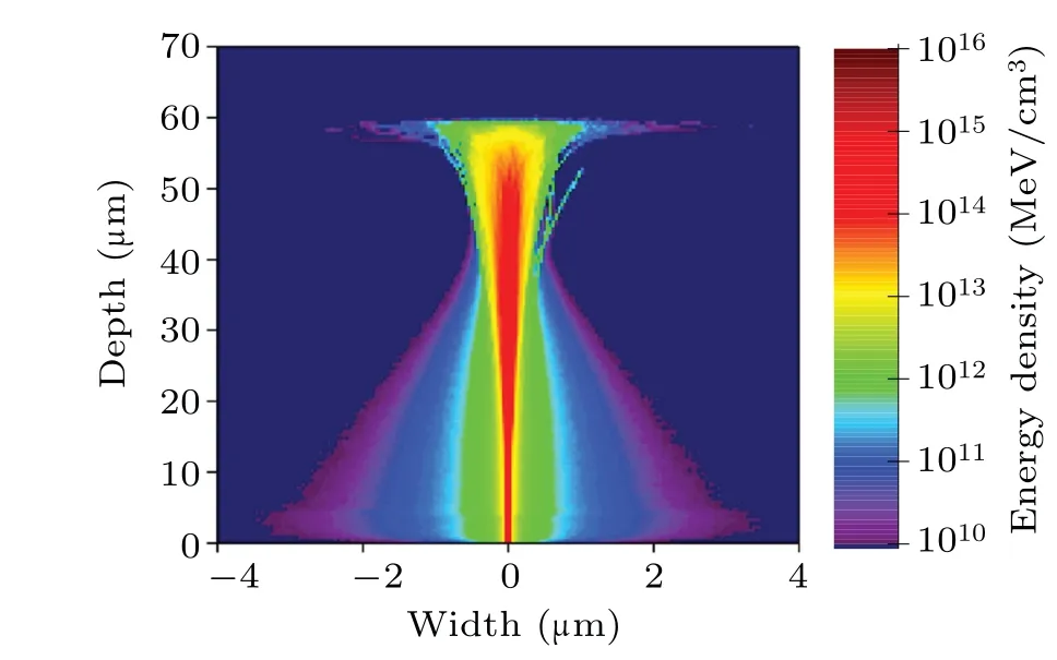
Fig.2. Distribution of energy deposition density in SiC.
The time-dependent cumulative energy deposition produced by heavy ions in SiC is shown in Fig. 3. In the simulation, the time is recorded when heavy ions strike on the upper surface of SiC.As time goes on, the energy deposition in SiC material increases exponentially. Heavy ions lose part of their energy when passing through Al, SiO2, and Si, and most of the energy is deposited in SiC. In about 2×10-12s,heavy-ion energy is exhausted,the secondary electrons in SiC also stop moving. The initial energy of Xe ions is 1217 MeV,and the energy deposited in SiC is about 1152.84 MeV. The spatial distribution and time parameters of energy deposition obtained by Monte Carlo simulation will be used in TCAD numerical simulation.
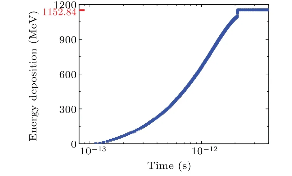
Fig.3. Time distribution of energy deposition in SiC.
3. Device numerical simulation
3.1. TCAD model setup
The device model of SiC MOSFET was constructed using TCAD simulation tools,the rated voltage and breakdown voltage of SiC MOSFET were 900 V and 1236 V,respectively.The gate voltage was 0 V in the subsequent simulations.In the simulation, Our main concern is the electrothermal effect of SiC MOSFET. The thermal conductivity, thermal resistance,and heat capacity parameters related to the electrothermal effect were modified according to the experimental results in the literature.[17,18]The thermal conductivity, thermal resistance, and heat capacity, respectively, follow the following formulas:[12]

whereTis the lattice temperature of SiC, other parameters used in TCAD simulation are given in Table 1.
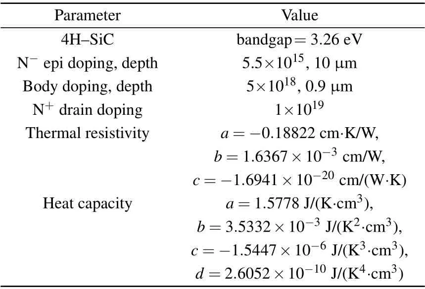
Table 1. TCAD simulation parameters.
The schematic diagram of simulating heavy ions perpendicularly incident on the SiC MOSFET is shown in Fig. 4.The cell structure of SiC MOSFET is symmetric, so the half cell structure of the device is selected for heavyion simulation in this work. In order to balance the on-resistance voltage and the breakdown voltage, the epitaxial layer of SiC power device varies in a range of 5 µm-15 µm in the application field of medium and low voltage.[7]According to the existing substrate thinning technology, the substrate thickness of SiC MOSFET can be less than 200 µm. The four positions in Fig. 4 are the four representative heavy-ion incident positions we selected. The first position indicates that the particles directly struck into the device from the epitaxial layer,the second position indicates that the particles pass through the channel and then enter into the epitaxial layer. The third position indicates that the particles enter through the source electrode,the channel region,and the epitaxial layer. The fourth position indicates that the particles enter from the body diode region of the device.At the same time,to explore the SEB sensitive area of SiC MOSFET,according to the maximum incident depth of Xe ion in SiC,the single event effect induced by Xe ion at four incident depths of 6µm,10µm,15µm,and 3µm were studied. The single event effect model parameters were obtained by Gaussian fitting of the particle transportation simulation results. When constructing the model,we refined the grid of the heavy ion track region.

Fig.4. TCAD simulation results of SiC MOSFET.
3.2. SEB sensitivity of MOSFET at different heavy-ion incidence positions
The melting point of SiC is generally in a range of 2900 K-3100 K.[12]In this simulation, it was assumed that its melting point is 3000 K, which is regarded as the critical temperatureTcfor SEB of SiC MOSFET.In the SEB sensitivity simulation of SiC MOSFET iat different incident locations,the depth parameter of heavy-ion incidence is 60µm,which is the Monte Carlo simulation result. In Ref.[19],SiC MOSFET reached a burnout condition and failed under the irradiation of Xe ion with energy of 1217 MeV. Figures 5 and 6 show the time and space distribution of the device lattice temperature when heavy ions strike from different positions. When the drain voltage is 800 V, SEB will occur when heavy ions strike from four positions. Affected by the incident position and drain voltage, the time to reach the critical temperature varies in the order of ps and ns. It takes the longest time to reach the critical temperature when heavy ions strike from position 2,the shortest SEB time occurs when incident position is position 3. When the leakage voltage was 300 V,the device’s lattice temperature can reach the critical temperature only at position 3. Based on the changes in the device’s lattice temperature under different voltages with time,position 2 and position 3 are the weakest incident position and the strongest incident position of SEB,respectively. When the incident strike comes from position 3,the gate-source junction of SiC MOSFET reaches the critical temperature first. When heavy ions strike from the other three positions, the substrate-epitaxial layer junction is the first area to reach the critical temperature.On the one hand,the local extremely high temperature affects the intrinsic properties of SiC. On the other hand, the high temperature may be transferred into the gate oxide layer and source electrode,affecting the performance of SiC MOSFET.The occurrence of high temperature at the electrode contact will cause the device’s electrical performance to degrade.[20]
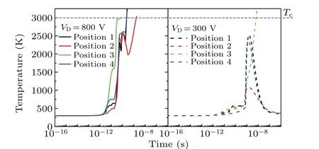
Fig.5. Time-dependent lattice temperature when heavy ions strike from different positions.
As shown in Fig.7,we have extracted the current distributions and the electric field distributions inside the device at different incident positions when the lattice temperature reaches the melting point. The power density, which is equal to the current density multiplied by the electric field,can reflect the power dissipation in the local area of SiC MOSFET.[13]Excessive power dissipation in a local area will cause the SiC lattice to melt. When heat is transferred into the SiC-metal interface and the metal contact,at the SiC-metal interface there occurs the lattice eutectic melting or the metal electrode melting.Combining with Fig.6,we can see that the area where the power dissipation occurs corresponds to the area where the critical temperature occurs. The distribution of current and the distribution of electric field is different from each other when the incident position of heavy ions changes.If a strong electric field and a large current exist in a local area of the device at the same time, excessive power dissipation will be generated in this area.
The distributions of time-dependent electric field,current density,and lattice temperature are extracted when heavy ions are incident from position 1 as shown in Fig.8.Driven by 800-V drain voltage, the electron-hole pairs generated along the heavy ion track recombine and move in the device,the current density in the source region and in the drain region gradually increase. At 260 ps,a strong electric field and a large current density occur at the substrate-epitaxial layer junction. The lattice temperature of SiC MOSFET first reaches the critical temperature in this area. It takes picoseconds to nanoseconds time for the lattice temperature of SiC to reach the critical temperature,while the time of device burnout is generally on the order of microseconds. The occurrence of excessive power dissipation under a specific drain voltage and the appearance of the corresponding lattice temperature are the cause of SEB in SiC MOSFET.

Fig.6. Spatial distributions of lattice temperature at different incident positions.

Fig.7. Current density and electric field distribution inside SiC MOSFET when lattice temperature reaches critical temperature under different incident positions.
Figure 9 shows the spatial distributions of device lattice temperature at different drain voltages. As the drain voltage decreases,the region in the device that first reaches the critical temperature shifts from the gate-source junction to the substrateepitaxial layer junction. It can be seen from Fig. 6, in the middle and low drain voltage range, burnout occurs mainly at the substrate-epitaxial layer junction. In Fig.5,only when the incident position is position 3,can the device reach the critical temperature during the first lattice temperature rise stage. When heavy ion strikes from the other three positions,the SEB appears at the second peak of the lattice temperature change. At the four heavy-ion incidence positions,the time-dependent lattice temperature has two temperature peaks. The first temperature peak appears at the gate-source junction, and the second one occurs at the substrate-epitaxial layer junction. If the values of all lattice temperature peaks are less than the critical temperature,burnout will not occur. The lattice temperature peak is related to the heavy-ion incident position,the magnitude of the drain voltage,and the LET value.

Fig.8. Electric field intensity,current density,and lattice temperature varying with time,with heavy ions striking from position 1.
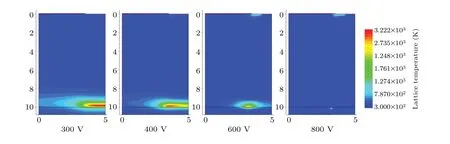
Fig.9. Spatial distributions of lattice temperature at different drain voltages,with heavy ions striking from position 3.
3.3. SEB sensitivities of SiC MOSFET at different heavyion incident depths
According to the distribution of Xe ion charge deposition density in SiC,calculated in the second part,the SEB simulations at four heavyion incident depths were carried out. The changes of the device lattice temperature with time under different incident depths are shown in Fig.10. When the incident depths are 10µm and 6µm,the lattice temperature under two drain voltage conditions cannot reach the critical temperature.According to the description in Fig.1,the epitaxial layer thickness of SiC MOSFET is 10 µm. When the incident depth of heavy ions does not exceed the epitaxial layer’s thickness,the lattice temperature is not high enough to reach the SEB critical temperature.
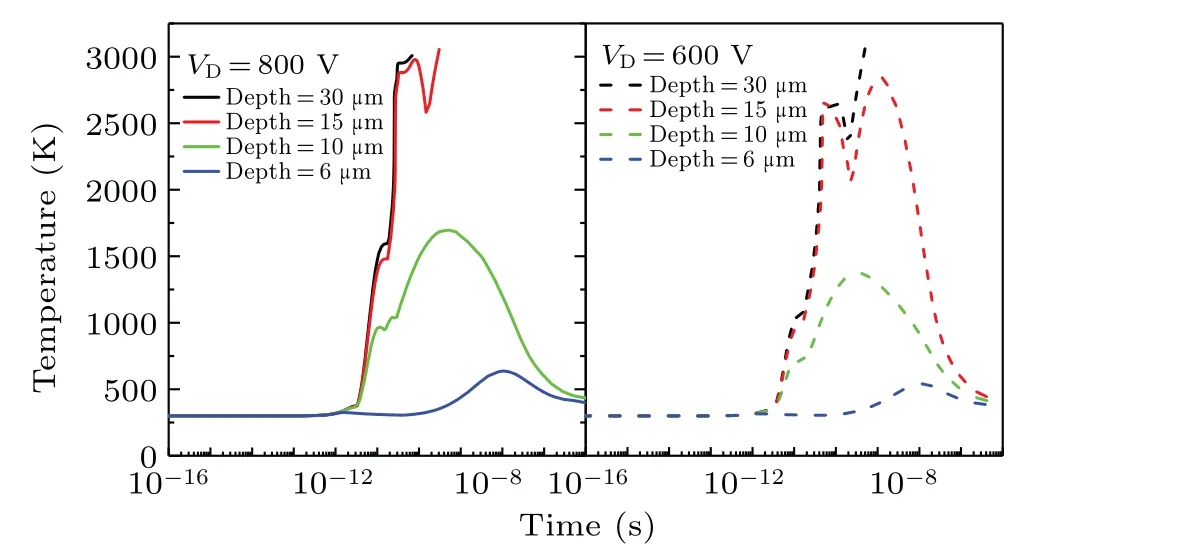
Fig.10. Lattice temperatures varying with time at different incident depths.
Figure 11 shows the time-dependent spatial distributions of the device lattice temperature when the heavy-ion incidence depth is 15µm at a drain voltage of 800 V.The time point of 8×10-11s corresponds to the first peak of the device lattice temperature in Fig. 10, which does not yet reach the critical temperature,and the time point of 3.11×10⁻¹⁰s corresponds to the time when the device reaches the critical temperature.As shown in Fig. 11, the first peak of lattice temperature appears at the gate-source junction of SiC MOSFET. This is the burnout area when the heavy ions strike from position 3 with 30-µm and 60-µm incident depths. When the incident depth is 15 µm, the lattice temperature in the gate-source junction is lower than the critical temperature. The burnout position finally appears at the substrate-epitaxial layer junction. The simulation results show that as the incidence depth of heavy-ions decreases,the SEB sensitivity of SiC MOSFET decreases. The SEB sensitive area of SiC MOSFET cannot be simply judged as the epitaxial layer.

Fig. 11. Lattice temperatures varying with time, with incident depth being 15µm.
4. Conclusions
By the Monte Carlo method,the spatiotemporal distribution of heavy-ion-induced energy deposition in SiC MOSFET is obtained. Using the TCAD numerical simulation,combined with Monte Carlo simulation results,the sensitivity of SEB in SiC MOSFET is analyzed. The coexistence of a large current and a strong electric field will cause excessive power dissipation and lead the lattice temperature of a local area of the device to exceed the melting point of SiC.The scenarios that heavy ions incident vertically on the SiC MOSFET at four different incident positions are simulated. When heavy ions are incident from the above source electrode, the device lattice temperature changes most obviously. the gate-source junction areas and the substrate-epitaxial layer junction area are both the initial areas in SiC MOSFET that reach the SEB critical temperature. The charge deposition in the epitaxial layer region of SiC MOSFET is not high enough to make the device’s lattice temperature reach the SEB critical temperature.
Acknowledgement
Project supported by the National Natural Science Foundation of China(Grant Nos.11875229 and 12075065).
猜你喜欢
杂志排行

Chinese Physics B的其它文章
- Superconductivity in octagraphene
- Soliton molecules and asymmetric solitons of the extended Lax equation via velocity resonance
- Theoretical study of(e,2e)triple differential cross sections of pyrimidine and tetrahydrofurfuryl alcohol molecules using multi-center distorted-wave method
- Protection of entanglement between two V-atoms in a multi-cavity coupling system
- Semi-quantum private comparison protocol of size relation with d-dimensional GHZ states
- Probing the magnetization switching with in-plane magnetic anisotropy through field-modified magnetoresistance measurement