Removal of GaN film over AlGaN with inductively coupled BCl3/Ar atomic layer etch
2022-01-23JiaLeTang唐家乐andChaoLiu刘超
Jia-Le Tang(唐家乐) and Chao Liu(刘超)
School of Physics and Electronic Engineering,Jiangsu Normal University(JSNU),Xuzhou 221116,China
Keywords: atomic layer etch,GaN,high electron mobility transistor
1. Introduction
AlGaN is widely used to construct AlGaN/GaN heterostructures to generate high-density two-dimensional electron gas(2DEG)for the applications in power electronics.[1-7]AlGaN is also used as a wide band gap electron barrier in light-emitting diodes and laser diodes.[4,8]In device manufacturing,it is difficult to achieve the uniform and precise height of the design pattern through conventional etching methods.[9]At the same time,it is usually necessary to keep the AlGaN(or AlN) layer in place.[10,11]For a normally-off enhancementmode high electron mobility transistor (e-HEMT) with a p-GaN gate, a p-GaN cap layer is grown on the AlGaN barrier layer to deplete the 2DEG in the GaN channel layer under the AlGaN barrier. To prepare the p-GaN gate and restore the 2DEG in the access area, it is necessary to completely and accurately remove the p-GaN cap layer in the access area. It is expected that the etching process will be smoothly stopped on the surface of the AlGaN barrier layer through a reproducible and easy-to-manufacture technology.[12-14]
In the industry, several studies reported on inductively coupled plasma (ICP) conventional etching GaN achieved,such as SF6/BCl3plasma with a GaN etching rate of 210 nm/min,[15]Cl2/Ar/O2plasma with a GaN etching rate of 550 nm/min,[16]Cl2/N2/O2plasma with a GaN etching rate of 320 nm/min,[17]and Cl2/N2/O2plasma, low ion bombardment,with a GaN etching rate of 45 nm/min.[18]These studies tried to fabricate enhancement-mode high electron mobility transistors with a p-GaN gate through a process which can etch GaN with a high selectivity over AlGaN.Compared with conventional etching, atomic layer etching has many advantages in uniformity and high aspectratio structure etching.[19,20]In recent years,some techniques for etching GaN in atomic layers have been proposed,such as etching GaN by being exposed to Cl2and Ar alternately,[21]etching GaN by being exposed to O2and BCl3alternately,[22]but atomic layer etching has never been used to fabricate enhancement-mode high electron mobility transistors with a p-GaN gate.
In this work, a new atomic layer etching process is proposed to remove GaN from AlGaN by being exposed to BCl3and Ar plasma alternately. In this work an etching depth is achieved to be 101 nm with the GaN etching rate of 0.73 nm/cycle.
2. Experiment
The atomic layer etching process was conducted in Leuven ICP2127 and the parameters were optimized to obtain an atomic layer etching GaN stop on Al0.2Ga0.8N, by using the samples of GaN/Al0.2Ga0.8N grown on sapphire substrates.The 11 cm2-sized samples were patterned by photolithography,and then etched with O2plasma.
Two kinds of structures GaN/sapphire (sample 1) and GaN/AlGaN/sapphire (sample 2) shown in Fig. 1, were used to study the etching of GaN stop on AlGaN in detail. Both structures were grown on 4-inch (1 inch=2.54 cm) sapphire substrates by metal-organic chemical vapor deposition. The thickness of GaN (sample 1) layer was 80 nm, the thickness values of GaN and AlGaN were 100 nm and 15 nm, respectively.
The etching depth and profile were characterized by scanning electron microscope (SEM, Regulus8220), revealed the mechanism of the self-limited etching which was characterized by x-ray photoelectron spectroscopy (XPS, Thermo Fisher),smoothness of AlGaN after being etched was characterized by atomic force microscope(AFM,Bruker Demension Icon).
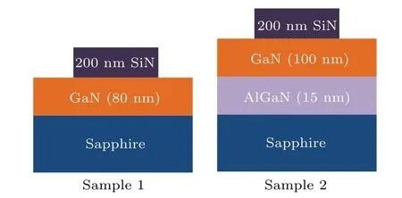
Fig.1. Schematic structures of sample 1 and sample 2.
3. Results and discussion
In order to verify the self-limitation of the process,the relationship between the modification time and the etching rate are studied, and the modification time is set to be 5, 10, 15,and 40-s per cycle. The etching time is fixed at 15 s, and the result is shown in Fig. 2. The results show that as the modification time increases, the time of exposure to BCl3plasma in each cycle of the first 10 s increases and the etching rate also increases. After 10 seconds, as the modification timeincreases, the etching rate per cycle is still about 0.74 nm per cycle. By extending the modification time, the etching depth will no longer increase, which indicates that the modification step is a self-limiting process.
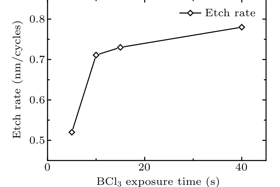
Fig.2. Etching depth per cycle of different modification time(5,10,15,and 40 s).
In order to confirm the self-limitation of the etching step,the relationship between the etching time and the etching rate is studied. The etching time is set to be 0, 5, 10, 15, and 40 s. and the modification time is fixed at 20 s. All results are shown in Fig. 3. In Fig. 3, extending the etching time at the beginning will increase the etching rate. When the etching rate is about 0.74 nm/cycles, the etching rate tends to be saturated. The etching depth of each cycle tends to be constant as the etching time increases. In this process,the etching step presents excellent self-limitation. As shown in Fig. 3,when the etching time is 0 s,the etching depth of each cycle is 0 nm. Like ALD,the realization of ALE has long been based on a series of independent,self-limiting surface reactions to replace the complex plasma-surface interactions of steady-state plasma etching. However, most of ALEs are not perfect, and there remain a small number of erosion etchimg cycles, and the etching steps in this article are completely self-limiting.Considering all the phenomena in Figs. 2 and 3 at the same time,after the plasma exposure time reaches a certain amount in the modification step and the etching step,the etching depth of each cycle tends to be constant,indicating that this process is a fully self-limiting process.

Fig.3. Etch depth per cycle for different etch time(0,5,10,15,and 40 s).
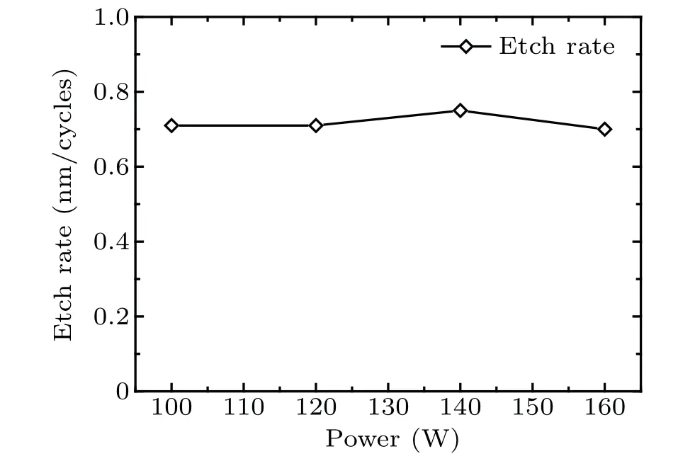
Fig.4. Etch depth per cycle of different power(100,120,140,and 160 W).
Because the etching step is a self-limiting step as shown in Fig. 3, when the etching time exceeds 15 s, the length of the etching time has little effect on the etching depth of each cycle. But in order to better control the process,the influence of the power in the process etching step on the etching depth of each cycle needs studying here in this section. The etching power is set to be 100 W,120 W,140 W,and 160 W,and the etching time is fixed at 15 s. All results are shown in Fig. 3.Figure 3 shows that increasing power has little effect on the etching rate.The reason for this is that the Ar bombardment in the etching step can completely remove the modified gallium chloride during the power change in this range. Therefore, it does not affect the etching rate.
Because the etching step is a self-limiting step,the length of the etching time as shown in Fig. 5 has little effect on the etching depth of each cycle.In order to make the etching depth of the entire process controllable, the research on the etching step is very important. Therefore, the influence of the bias voltage in the process etching step on the etching depth of each cycle is investigated. The etching bias is set to be 20 V,30 V,40 V,and 50 V,and the etching time is fixed at 20 s.All results are shown in Fig.5.With the increase of the bias in the etching step,the etching depth per cycle increases slightly. The reason for this is that the bias voltage increases and the ion gains a greater acceleration. Owing to the increase in bombardment energy,after the modified layer is completely removed,the remaining ion bombardment will continue to produce a small amount of physical etching on the GaN surface.

Fig.5. Etch depth per cycle of different bias(20,30,40,and 50 V).
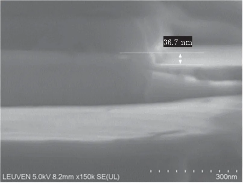
Fig.6. Morphology of GaN surface after 50 cycles of BCl3/Ar plasma etching.
After the above experiment,the modification time is set to be 15 s,the etching time 20 s,the etching source power 120 W,and the etching bias 20 V.The sample 1 is etched for 50 cycles under this parameter. The etched morphology of the GaN surface,measured by SEM,is shown in Fig.6. The etching depth is 36.7 nm, and the etching rate is calculated to be 0.73 nm per cycle. The BCl3plasma will modify the GaN into gallium chloride on the GaN surface, and then the Ar plasma is used to bombard the surface, thus the modified gallium chloride is removed from the surface. Before etching, there is a 200-nm SI3N4serving as a hard mask to form a pattern on the surface.
When using BCl3/Ar plasma to cyclically etch GaN, the chlorination time is set to be 15 s, the etching time 20 s, the etching power 120 W, and the etching bias 20 V, the process of this parameter is applied to etching sample 2. The result is shown in Fig. 7. Figure 7(a) shows a cross-sectional view of sample 2 after 137 cycles of etching. The etch depth of GaN is 102 nm, and the surface damage to AlGaN is only 2 nm.Figure 7(b)is an oblique view of sample 2 after etching. It can be observed that the surface of sample 2 is flat and smooth.
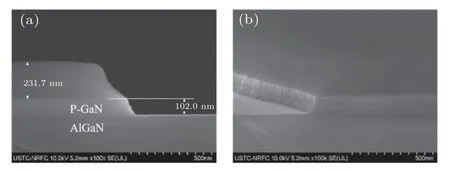
Fig. 7. (a) Cross-sectional view of sample 2 after etching, and (b) oblique view of sample 2 after etching.

Fig.8. (a)Topography of(a)3µm×3µm surface of GaN before etching and(b)5µm×5µm surface of AlGaN surface after etching.
After 137 cycles of etching, the surface is accurately stopped on the AlGaN surface, and on the basis of meeting the requirements of the device in terms of morphology, the atomic force microscope (AFM) is used to characterize the surface before and after the etching. The GaN before etching and the AlGaN after etching are characterized,and the results are shown in Fig.8. Figure 8(a)shows the topography of the 3 µm×3 µm surface of GaN before etching, and its average roughness is 2.94 nm. Figure 8(b)displays the topography of the 5 µm×5 µm surface of the AlGaN surface after etching,with an average roughness of 1.78 nm. It can be seen from the measurement results that this process meets the requirements of device design from the perspective of surface roughness.

Fig.9. Ga(3d)CL spectra observed at different values of bond energy of 17.5 eV,19.2 eV,and 18.6 eV for the initial sample,sample modification,and sample etching,respectively;deconvoluted Ga(3d)XPS spectra of(b)initial sample,(c)modified sample,and(d)etched sample.
In order to study the chemical state and the interaction between the chemically adsorbed chlorine and the film surface,XPS is used to characterize the chemical state of the GaN surface of different samples,and the results are shown in Fig.9.Figure 9(a) shows the peak positions of the XPS Ga (3d) CL spectra observed at different values of bond energy of 17.5 eV,19.2 eV,and 18.6 eV for the initial sample,sample modification, and sample etching. As shown in Fig. 7, the characteristic peak of Ga-Cl does not appear in the peak coupling of the initial Ga(3d)CL spectrum of the sample,but occurs after BCl3plasma modification. After the etching step, the Ga-Cl characteristic peak disappeared.
According to the characterization analysis of XPS, the etching mechanism of BCl3/Ar plasma anisotropic atomic layer is shown in Fig. 10. It indicates that there is no chlorine on the GaN surface at the initial stage. After ICP plasma chlorination,chlorine is adsorbed on the surface. At the etching step,owing to the low-energy bombardment of Ar plasma,the adsorbed chloride on the surface is removed. The modification of the process is that chlorine gas adsorbs on the surface to form a chlorinated layer,and then Ar low-energy bombardment removes the chloride. BCl3/Ar plasma anisotropic atomic layer etching is the repeating of the process.

Fig.10. Schematic diagram of BCl3/Ar plasma anisotropic atomic layer etching mechanism.
4. Conclusions and perspectives
In this paper,BCl3plasma cycle and Ar plasma cycle are used to etch GaN alternately, and the self-limiting of atomic layer etching is used. The etching depth of each cycle is about 0.73 nm,and the etching is controlled precisely by controlling the number of etching cycles. As a result,the etching process accurately stops on AlGaN after removing the GaN.This technology can provide a new and repeated manufacturing process for enhancement mode high-electron-mobility transistors with P-GaN gates.The O2plasma etching process and BCl3plasma etching process are both self-limiting process for the change of chlorination time parameters and also self-limiting for other parameters. It is not sensitive to the changes of other process parameters, so it has extremely high stability. Limited to the experimental conditions, its electrical properties, and the actual device performance still need firther verifying.
Acknowledgements
Project supported by the National Foreign Experts Bureau High-end Foreign Experts Project, China (Grant No.G20190114003),the Key Research and Development Program of Jiangsu Province,China(Grant No.BE2018063),the Natural Science Research Projects of Colleges and Universities in Jiangsu Province, China (Grant No. 19KJD140002),and the Scientific Research Program for Doctoral Teachers of JSNU,China(Grant No.9212218113).
猜你喜欢
杂志排行

Chinese Physics B的其它文章
- Superconductivity in octagraphene
- Soliton molecules and asymmetric solitons of the extended Lax equation via velocity resonance
- Theoretical study of(e,2e)triple differential cross sections of pyrimidine and tetrahydrofurfuryl alcohol molecules using multi-center distorted-wave method
- Protection of entanglement between two V-atoms in a multi-cavity coupling system
- Semi-quantum private comparison protocol of size relation with d-dimensional GHZ states
- Probing the magnetization switching with in-plane magnetic anisotropy through field-modified magnetoresistance measurement