Magnetic polaron-related optical properties in Ni(II)-doped CdS nanobelts: Implication for spin nanophotonic devices
2022-01-23FuJianGe葛付建HuiPeng彭辉YeTian田野XiaoYueFan范晓跃ShuaiZhang张帅XianXinWu吴宪欣XinFengLiu刘新风andBingSuoZou邹炳锁
Fu-Jian Ge(葛付建) Hui Peng(彭辉) Ye Tian(田野) Xiao-Yue Fan(范晓跃) Shuai Zhang(张帅)Xian-Xin Wu(吴宪欣) Xin-Feng Liu(刘新风) and Bing-Suo Zou(邹炳锁)
1Beijing Key Laboratory of Nanophotonics and Ultrafine Optoelectronic Systems,School of Physics,Beijing Institute of Technology,Beijing 100081,China
2CAS Key Laboratory of Standardization and Measurement for Nanotechnology,CAS Center for Excellence in Nanoscience,National Center for Nanoscience and Technology,Beijing 100190,China
3University of Chinese Academy of Sciences(CAS),Beijing 100049,China
4Guangxi Key Laboratory of Processing for Non-ferrous Metals and Featured Materials,School of Resources,Environments and Materials,Guangxi University,Nanning 530004,China
Keywords: dilute magnetic semiconductor,exciton magnetic polaron,photoluminescence,antiferromagnetic magnetic polaron
1. Introduction
Room temperature magnetic semiconductors have been listed as one of the most urgent and important 125 scientific challenges in the way of human development.The spin-related carriers and excitons hence become the focus of their studies,especially the latter. The diluted magnetic semiconductors(DMSs) have been found to be a series of room temperature magnetic semiconductors. The optical properties of DMSs have aroused tremendous research interest,especially in transition metal(TM)-doped II-VI semiconductors. The extraordinary magnetic polarons’ luminescence behaviors and various d-d transition emissions in DMSs open new paths for the development of displays, bosonic lasers, and even spintronic devices.[1]
The incorporation of transition metal brings up some new properties due to the spin-spin,spin-lattice,and spin-exciton interactions. Different magnetic polarons, like exciton magnetic polaron (EMP),[2]bound magnetic polaron (BMP),[3]antiferromagnetic polaron (AMP),[4]paramagnetic polaron(PMP) can form in the local doping area, leading to different optical and transport behaviors. Therefore, the uniform distribution and/or type of doping ions are crucial to determining the excitation nature and related physical properties.[2]For example, the strong electron-phonon coupling by the doping elements in DMS usually causes local lattice distortion and polarization, which may exhibit varied properties for different spin-spin couplings.[4]In DMSs, the localized polarization field is mostly a magnetic field produced by ferromagnetic coupled ions. Electrons or holes move with the magnetic field to form composite particles,which are called magnetic polarons. If the spin coupling between the doped TM ions can form a ferromagnetic (FM) polarization field, and free excitons can couple with the ferromagnetism and longitudinal optical (LO) phonons to produce exciton magnetic polarons[2,5](EMPs). Excitons bound by donor defects or acceptor defects can couple with magnetic ions to form bound magnetic polarons[3,6](BMPs). The direct exchange interaction between BMPs(BMP-BMP)is also normally FM.Thus it can be seen that FM magnetic polarons are more common,and there are far fewer reports on antiferromagnetic magnetic polaron[4](AMP)due to the existence of nearby defects or local carriers. Therefore, using requisite optical and magnetic response[7]methods to study the EMP, BMP, AMP or other antiferromagnetic elementary excitations at low doping concentration will help fill in the gaps between semiconductor and magnetism, and have a better understanding of the properties of magnetic polarons.
Cadmium sulfide (CdS), a group II-VI semiconductor with a band gap of 2.42 eV at room temperature(RT),has excellent crystallinity,luminescence and transport properties.[8]Recently TM-doped CdS has garnered increased attention due to its unique optical properties, such as the bosonic lasing of EMPs by doping with Cu,[9]and tunable trap state emissions by doping with Sn.[10]Compared with Cu and Sn,Ni2+is unusual due to its eight electrons in the 3d orbital. Owing to the quantum confinement effect or the strong covalent bond effect of p-d hybridization,dilute Ni-doped or co-doped[11,12]materials may result in better optical and magnetic properties. In the past, many studies have focused on the near-infrared luminescence of Ni-doped DMSs(such as CdS[13]and ZnS[14]).However,the visible range with the strongest luminescence at low doping concentrations has often been neglected. Therefore,this work focuses on the optical properties of the visible range of Ni-doped CdS.
In this work, we use pure CdS and NiI2powders as precursors;Ni-doped CdS nanobelts(NBs)are prepared using the chemical vapor deposition(CVD)method. Subsequently, the macroscopic optical properties and microscopic mechanisms of the as-grown sample are studied using the magnetic hysteresis loop, micro-PL, femtosecond (fs) laser, and XPS. In addition to the condensation of EMPs,some free excitons unexpectedly form antiferromagnetic magnetic polarons(AMPs)through AFM coupling at low temperatures, which has never been reported in a CdS lattice. Meanwhile, two special PL peaks related to another EMP emission and d-d transition of antiferromagnetically coupled Ni2+-Ni2+pairs also appear at higher doping concentrations. Based on the above results,Nidoped CdS appears to be a type of DMS with special and novel properties,which deserves further investigation.
2. Experiment details
A sample of high-quality Ni-doped CdS NBs was prepared via CVD. Typically, 0.3 g of CdS powder and an appropriate amount of NiI2powder were added to the grinding bowl and ground thoroughly to obtain the precursor. Then,the precursor was placed in the quartz tube,and a 13-sccm flow of argon-hydrogen gas mixture(~5%hydrogen)was passed into the quartz tube. The precursors were heated to 1050°C over a period of 15 min and held at 1050°C for 60 min. Subsequently,the furnace was naturally cooled to RT,and Ni-doped CdS NBs were obtained.
The morphology was characterized using a scanning electron microscope(SEM)(Zeiss SUPRA 55)equipped with energy dispersive spectroscopy (EDS). The magnetic hysteresis loop was obtained using a vibrating sample magnetometer(VSM)(Lakeshore,730T,USA).The phase purity was investigated using x-ray diffraction(XRD)(PANalytical,Empyrean,Netherlands). Surface studies were performed on x-ray photoelectron spectroscopy(XPS)(VG Scientific ESCALAB-210 spectrometer, East Grinstead, UK) with monochromatic MgKαx-rays(1253.6 eV).The micro-PL and micro-Raman spectra were obtained using a laser confocal microscope system (Acton SP2500, Olympus BX51M, Princeton Instruments) with an excitation source of 405-nm or 532-nm laser.Temperature-dependent PL spectra were obtained using a liquid helium-cooled system. The femtosecond laser test in which a 400-nm pulse laser was used as an excitation source,which was generated by a barium borate crystal(BBO)to double the frequency from the Coherent Astrella (center wavelength: 800 nm,100 fs,1 kHz)amplifier.
3. Results and discussion
Figure 1(a)shows the collective morphology of the grown samples. The grown NBs are on the order of several microns in width and dozens of microns in length. Figure 1(b)depicts the morphology of a single Ni-doped NB, which exhibits a smooth surface. There is no metal ball present on the top surface of the NB, indicating that the growth mechanism of the sample is vapor-solid(VS)process rather than vapor-liquidsolid(VLS)process. The NBs grow from a gaseous state to a solid state directly on the substrate at high temperatures. Remarkably,the concentration of S and the concentration of I of the NBs are lower than those of CdS and NiI2(Fig.1(c)and its illustration). In the growth process, hydrogen reacts, respectively,with S and I to produce gaseous H2S and HI,which are blown away by a mixture of argon and hydrogen.[15]The elemental maps of Figs.1(d)-1(g)also suggest that Ni is evenly distributed throughout the NB. Moreover, the concentrations of S and I decrease,which concurs with predictions.
To confirm the magnetic properties of the DMS, the magnetic hysteresis loops of the samples were measured at RT. The applied magnetic fieldHranges from-10000 Oe(1 Oe=79.5775 A/m) to 10000 Oe; the results are shown in Figs.2(a)and 2(b). As observed,the curves show distinct FM behaviors.The saturation magnetizationMsand coercive forceHc(49, 70, 95 Oe)of the samples increase markedly with Ni concentration increasing. However,the ferromagnetism is not quite large,which may be attributed to the dilute doping of Ni and the small AFM order inside the lattice. Both the cobaltdoped CdS experimental results[16]and TM-doped CdS theoretical calculations[17]confirm that the Curie temperature of TM-doped CdS significantly exceeds RT,which indicates that Ni-doped CdS can achieve room-temperature ferromagnetism.

Fig. 1. (a) Low-magnification scanning electron microscopy image of Nidoped CdS NBs. (b) High-magnification SEM image of a single Ni-doped NB.(c)Energy dispersion spectroscopy(EDS)image corresponding to pink box area in panel (b). (d)-(g) Elemental mapping of Ni-doped NB in pink box area in panel(b).

Fig. 2. (a) The M-H curves of Ni-doped CdS NBs at RT, and (b) partially enlarged view of M-H curves in panel(a).
In small-sized nanocrystals such as quantum dots(QDs),the ferromagnetic order tends to split into small pieces with different spin directions, forming superparamagnetism rather than ferromagnetism.In the SEM and EDS results of our sample,the S content is much smaller than that of Cd,confirming the presence of some defects. In the reaction process at high temperature, there are some hydrogen molecules to work as the carrier gas and protecting gas, so the H2S can be formed to leak out with carrier gas. So the deposited CdS contains less S inside the lattice. Therefore, the content of sulfur in the nanobelts is lower than that of cadmium,and a number of sulfur vacancies will be generated. That is to say,owing to the lower boiling point of S and gaseous H2S,part of the S will escape from the surface of as-formed products at high temperature during the growth of the nanobelts,thereby forming some S vacancies.[18]In previous report,[19]the content of S exceeds that of Cd. This is related to the high Ni doping concentration and the large amount of substitution of Cd. The doping concentration of Ni in our sample is relatively low (lower than 2%),and Ni does not substitute Cd in a large amount. So the content of S does not exceed that of Cd, which has also been confirmed in the similar experiments.[15]
Within bulk nanocrystals such as NBs, defects’ movement and carriers’ movement can act as intermediaries, leading to exchange interactions between isolated spin magnetic moments. These exchange interactions contribute to ferromagnetism[20]and prevent TM-doped DMSs from becoming paramagnetic materials. Meanwhile,some new peaks appear in the low-temperature PL spectra (Fig. 4), proving the existence of antiferromagnetism,which can also affect the magnetism. During the movement in the lattice, the photoinduced free excitons couple with the FM Ni-ion pair,forming a local ferromagnetic EMP.When a free exciton combines with the AFM Ni-ion pair,an antiferromagnetic polaron(AMP)is formed. In other words, the ferromagnetism of the sample is considerably stronger than the antiferromagnetism at RT,which further indicates that ferromagnetic EMPs dominate the luminescence at RT. The above analysis is verified further in the micro-PL spectra.
Figure 3(a) shows the XRD patterns of Ni-doped CdS NBs,and all the diffraction peaks of the as-synthesized sample match well with the wurtzite hexagonal structure(JCPCD#41-1049). The diffraction peaks are narrow and sharp without splitting,and the signal quality is strong,indicating good crystallinity within the as-prepared sample. This is one of the advantages of CVD.It is worth noting that the diffraction peaks shift toward higher angles with Ni concentration increasing.This is because the ionic radius of Ni(0.69 ˚A)is smaller than that of Cd(0.95 ˚A),[21]resulting in a slightly deformed lattice structure.

Fig.3. (a)X-ray diffraction patterns of pure CdS(JCPCD#41-1049)and Ni-doped CdS NBs with different Ni concentrations. (b)RT micro-Raman spectra of NBs with different Ni concentrations. (c)XPS survey and(d)Ni 3s XPS spectra of Ni-doped CdS nanobelts.
Raman spectra can be used to study phonon vibration modes and identify lattice defects. The interaction between carriers and phonons involves two main mechanisms: the deformation potential and the Fr¨ohlich potential. The deformation potential is mainly the short-range interaction between acoustic phonons,[22]while the Fr¨ohlich potential is mainly the long-range interaction between the macroscopic electric field of electrons (excitons) and longitudinal optical(LO) phonons.[23]As observed in Fig. 3(b) and Table 1, the peaks at approximately 308 cm-1and 604 cm-1can be ascribed to the LO phonon mode and 2LO phonon mode,[16]respectively. As the Ni doping concentration increases from 0.65%to 1.86%,the LO mode blueshifts from 305.7 cm-1to 309.9 cm-1, this shift is about 4.2 cm-1, and the 2LO mode blue-shift is 0.6 cm-1. The LO peak of Zn-doped CdS[24]also blueshifts with the increasing doping concentration,while that of Sm-doped CdS[25]redshifts with the doping concentration increasing. This opposite phenomenon is associated with the difference in ionic radius between doped ions and Cd2+.In the Ni-doped CdS, the shift of LO peak is attributed to the ionic radius of Ni2+smaller than that of Cd2+,which leads the lattices to shrinke,and the bonds to strengthen,which causes the resonance frequency to increase.[25]The intensity ratio of the 2LO mode to the LO mode,2LO/LO,indicates the strength of the Fr¨ohlich coupling between excitons and phonons,namely electron-phonon coupling. The value of 2LO/LO increases with Ni concentration increasing as shown in Table 1. The incorporation of Ni strengthens the scattering between LO phonons and electrons, enhancing the long-range interaction inside the lattice, which further promotes the Fr¨ohlich coupling between electrons and phonons.
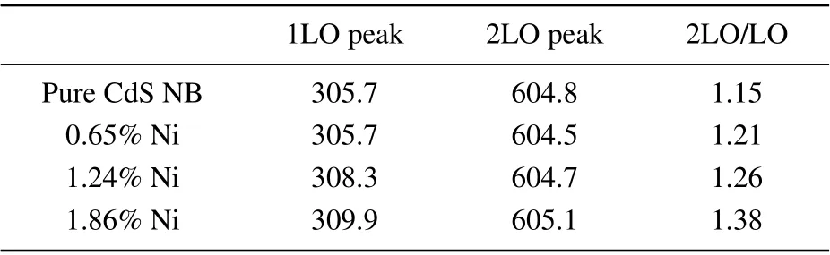
Table 1. Phonon modes(in unit cm-1)derived from Fig.3(b).
Figures 3(c) and 3(d) show XPS survey and Ni 3s XPS spectra of Ni-doped CdS nanobelts. The peak at 111.74 eV can be assigned to Ni 3s state, which indicates that Ni atoms have been doped into CdS lattice successfully.A spectral analysis using curve fitting is shown in Fig.3(d). The binding energy values of N 3s and N2+3s are 110.62 eV and 111.68 eV,respectively. The fitted spectrum clearly shows that the main contribution comes from N2+,which indicates that most of the Ni ions in the Ni-doped CdS nanobelts are Ni2+.[26,27]
The optical properties of Ni-doped CdS NBs can be studied by observing Fig.4,which shows the micro-PL spectra of the NBs under the excitation of a 405-nm continuous wave.From Fig. 4(a) it can clearly see that the EMP peak gradually appears and is enhanced with the increase in Ni doping concentration, which is related to the doping and coupling of Ni2+cations. Moreover, in Ni-doped CdS NBs the lack of S is notable, which causes the donor levels in the conduction band to degenerate and merge. The conduction band expands into the band gap,and thereby,the band-edge emission is red-shifted.[28]When more Ni2+ions are doped into the CdS lattice, the defects of the crystal increase. At RT, more isolated spin magnetic moments (due to Ni doping) will use more defects as media to couple together and produce stronger exchange interactions,[29]which produces stronger RT ferromagnetism and more EMPs. Therefore,the higher the Ni doping concentration, the greater the redshift of the band-edge peak is. Simultaneously, the EMP to FX peak intensity ratio also increases.
Figure 4(b)shows the temperature-dependent PL spectra near the band edge. The emissions near the band edge are blue-shifted due to the lattice shrinkage and weaker electronphonon interaction with temperature decreasing,which is consistent with the band-edge temperature-dependent characteristic obtained from the Varshni formula.[30]Surprisingly,a new peak appears at the higher-energy end of the FX peak at 180 K,and a new peak occurs at approximately 530 nm. When the temperature drops to 80 K,there appear four peaks at 496 nm,499 nm (FX), 509 nm (EMP1), and 530 nm (EMP2) in the range of 490 nm-530 nm.
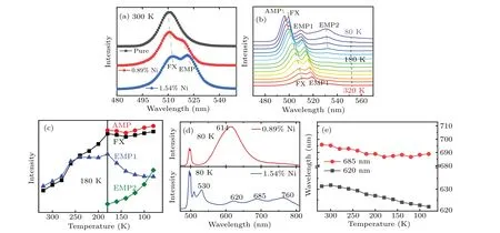
Fig.4. (a)Micro-PL spectra of CdS NB with different Ni concentrations in a range of 480 nm-550 nm at RT.(b)Temperature-dependent PL spectra of CdS NB with Ni concentration of 1.54%in range of 470 nm-570 nm. (c)PL intensity versus temperature in panel(b). (d)Micro-PL spectra of CdS NB with different Ni concentrations at 80 K.(e)Wavelength versus temperature for the two peaks in panel(d).
As for the peak at 496 nm, the pure CdS nanobelts do not show this peak at low temperature,[8]indicating that this peak is introduced by Ni doping. We attribute the 496-nm peak to a new excitation of coupling between free excitons and antiferromagnetically coupled Ni-ion pairs or clusters,defined as antiferromagnetic magnetic polarons(AMPs). This is because when TM-doped ions are ferromagnetically coupled,the band edge will be red-shifted, but when they are antiferromagnetically coupled, they will be blue-shifted.[9]There is also a strong electron correlation between AFM-coupled Ni ions,resulting in an increase in energy above the band gap.[31]Furthermore, the low formation energy encourages antiferromagnetically coupled pairs or clusters to often interact with the doped TM ions, which promotes the formation of AFM excitations. The 496-nm peak may be attributed to a BMP emission or an LO phonon replica emission. The formation of BMP requires defects or TM dopants to bind with excitons to prevent dissociation. In this case,more excitons should be bound rather than free at higher power at RT. A broadening of exciton absorptions will occur,[32]that is,a blueshift under higher-power fs pulse excitation. However,we do not observe this in the following test,and thus the 496-nm peak cannot be a BMP-related emission.As for the LO phonon replica emission guess, this emission is normally observed on the low-energy side of the FX peak. The energy span between the 496 nm and FX peak at 80 K is only 18 meV,which is much lower than the LO phonon energy.
The emission band at 530 nm is attributed to another EMP emission.To distinguish them,we label 509 nm and 530 nm as EMP1 and EMP2, respectively. In a previous report,[33]with a higher Ni concentration(2%-4%),the EMP2 emission dominated in the RT PL spectra when a high concentration of Ni was doped in CdS. In our sample, there is no obvious emission band near 530 nm when the concentration of Ni is 0.89%,but it does exist when the concentration of Ni is 1.54%as depicted in Fig.4(d). The appearance of the EMP2 emission is related to the higher Ni doping concentration. It is easy to notice the large energy span between the 530-nm peak and the band edge. Predominantly, more Ni ions can bring stronger FM coupling, which can bind with more LO phonons and cause larger redshifts and larger full width at half maximum(FWHM). In addition, doped I ions can result in a chargetransfer effect or the formation of exciton complexes, which contributes to a larger redshift. The electron-phonon coupling weakens because of the attenuation of nonradiative recombination at low temperatures,[34]that is,LO scattering is weakened,which results in the enhancement and coexistence of the two EMP-related emissions. Hence,more Ni ions can present stronger FM coupling,enhancing the emission of EMP2.
In Fig. 4(c), the AFM magnetization becomes stronger gradually with temperature decreasing, which is the reason why the AMP peak appears only at low temperatures. Moreover, this phenomenon also confirms that the AFM layers’coupling between the FM layers in the NiI2crystal is pronounced only at low temperatures.[6]Notably, the intensity of the EMP1 peak increases from 320 K to 180 K. However, when the EMP2 emission comes out, the EMP1 emission decreases,indicating that there is competition among free excitons and that the EMP2 emission dominates at low temperatures. The antiferromagnetism gradually increases with temperature decreasing. In addition, more free excitons couple with antiferromagnetic Ni ion pairs to form AMPs, contributing marginally to the weakening of the EMP1 peak below 180 K.
In Fig.4(d),one can see that the NB with 0.89%Ni concentration has a 614-nm luminescence peak at 80 K, which is caused by the d-d transition (1Eg→3A2g) of the single Ni2+.[35]However, for the NB with 1.54% Ni concentration,there are three main peaks at 620 nm, 685 nm, and 760 nm,respectively. The emission peak at 620 nm is close to 614 nm,so they should have the same origin. Herein, we attribute the emission at 685 nm to the d-d transition of the AFM Ni2+-Ni2+pair. In this case, strong spin-orbital coupling and sp-d hybridization affect the d-d transition of the lattice vibrations.[36]For the 685-nm peak with the Ni-S-Ni AFM pair, the dipole-polarized orientations of the two phonons in the Ni-S vibrations are antiparallel,which causes them to cancel each other’s influences on energy.[37]Thus, the peak at 685 nm has no consistent shift at low temperatures as depicted in Fig.4(e). The 760-nm peak is another d-d transition emission(3T1g→3A2g)of Ni2+,which has been verified in previous work.[16]
To further study the power-dependent properties of EMPs and AMPs, a 405-nm continuous wave laser is used to excite the Ni-doped CdS NB with 1.54% Ni concentration at 80 K.The intensity of the EMP2 peak does not change significantly,so it is not shown. In Fig. 5(a), as the power increases from 0.92 mW to 3.77 mW,the redshifts of the AMP peak,the FX peak and the EMP peak are 4.0 nm, 2.5 nm, and 0.7 nm, respectively. These redshifts originate from the increasing carrier concentration in the Ni-doped CdS NB with the increasing of excitation power,which renormalizes the CdS band gap.[38]Moreover, the distinction between AMP and FX is no longer obvious when the excitation power reaches 3.7 mW.The peak positions and relative intensity of the two peaks at 3.7 mW are similar to those at 160 K. It is speculated that a certain amount of heat occurs in the lattice under the excitation of a higher-power continuous wave. Figure 5(b) shows that as the excitation power increases,the EMP has a significant blue shift before 1.36 mW. At a low carrier density, the blueshift caused by the screening effect of the Coulomb potential[38]exceeds the redshift produced by band-gap renormalization.As the excitation power increases, the carrier density further increases, and the redshift induced by band gap renormalization gradually became dominant. The decrease in the intensity ratio of EMP to FX (IEMP/FX) below 1.36 mW indicates that when the lattice heating is not obvious, the AFM Ni2+-Ni2+pair has a stronger coupling effect with the carriers than the FM Ni2+-Ni2+pair at low temperatures, indicating that there is competition for carriers between ferromagnetism and antiferromagnetism. With the further increase of the excitation power,IEMP/FXrises rapidly. When the lattice heating becomes more severe, the antiferromagnetism is less likely to couple with free excitons. In contrast,ferromagnetism can couple with more free excitons to form EMPs, and via longrange FM interactions,a more intensely emitting coherent aggregate arises gradually.

Fig.5.(a)Power-dependent PL spectra excited by a 405-nm continuous wave laser at 80 K.(b)Peak position and intensity of EMP and FX in panel(a).
The fs pulse laser can detect the scattering among magnetic polarons,carriers,and phonons,as well as the excitation and relaxation processes on a very short spatiotemporal scale.The room-temperature fs lasing results of the Ni-doped CdS NBs are shown in Figs.6(a)-6(c). Figure 6(a)shows an obvious double-peak characteristic. Using the Varshni formula[39]Eg(T)=Eg(0)-αT2/(T+β),when the exciton-A band-gap energy at 0 KE0A=2.550 eV is substituted intoEg(0), the result of the exciton-A band-gap energy at 300 K is 2.474 eV(501.2 nm). This coincides with the peak position of the left peak at low excitation power (82.997 µJ/cm2), which proves that the left peak is indeed the free exciton(FX)peak. However, under continuous-wave excitation, the crystal is easily heated to an extent enough to cause band-edge emission redshifts. In comparison, the excitation of femtosecond lasing does not cause significant heat accumulation in the crystal.Furthermore,the energy span between the FX peak(2.474 eV)and the right peak(2.404 eV) is 70 meV when the excitation power reaches 165.994 µJ/cm2as shown in Fig. 6(b). It is much larger than the 1LO(A1)phonon energy(38 meV),and thus it cannot be attributed to a phonon replica emission.[40]This low-energy peak originates from EMPs. At RT, the Nidoped CdS NBs exhibit ferromagnetism, and only ferromagnetism can reduce the energy of free excitons, so this lowenergy end peak is an emission related to ferromagnetism and free excitons.[41]The energy span is also close to the 2LO A1phonon energy (75 meV), which indicates that the 2LO (A1)phonons participate in the polarization process of the EMPs rather than the 1LO(A1)phonons.
Then, three fitting curves are obtained using Gaussian fitting as shown in Fig. 6(a), and the sum of the three fitting curves is in good agreement with the actual value. The GFC1 and GFC2 correspond to FX and EMP,respectively,because their relative positions and peak widths coincide with the counterparts of continuous-wave PL spectra. The EMPs tend to form a coherent aggregate emitting a sharp peak in the spectrum;thus,the width of GFC2 is narrow. The GFC3,which is closer to GFC2 and seemingly wider, should be primarily related to the effects of bound carriers interacting with EMPs due to the doping of I in the preparation stage.
Figure 6(b) displays the lasing profiles of the Ni-doped NBs under different excitation power values. With the increase of pump density, the Ni-doped CdS NBs exhibit an obvious single-mode coherent lasing characteristic. The FX peak rapidly decreases in comparison with the EMP peak,which shows that there are more free excitons combined with LO phonons and FM domains to form EMPs. An increasing number of EMPs form coherent aggregates, which show the characteristics of narrower FWHM, nonlinear intensity, and single-mode lasing. Figure 6(c) shows the FWHM and peak intensity against the increasing pump density of the femtosecond laser. When the pump density exceeds 132.796 µJ/cm2,the FWHM of the EMP peak at the low-energy end narrows rapidly. When the pump density reaches 175.124µJ/cm2,the FWHM shrinks sharply,reaching only~1 nm. The intensity also begins to increase rapidly simultaneously, and the variations exhibit nonlinear characteristics.When the pump density exceeds 175.24 µJ/cm2, the FWHM no longer narrows, and even slightly increases. At the same time,the lasing peak also exhibits a slight redshift as depicted in Fig. 6(b). It is speculated that these phenomena are related to a small quantity of photoinduced electron-hole plasma(EHP),[42]which reinforces the electron-electron collision and the electron-phonon interaction. The carrier effect produced by this EHP also makes a small contribution to the existence of GFC3 as shown in Fig.6(a).
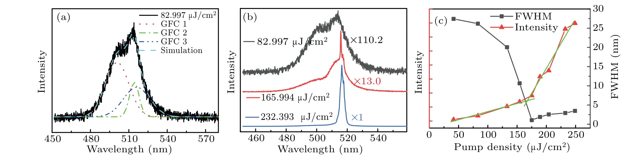
Fig.6. PL spectra excited by 400 nm fs pulse laser at RT,showing(a)PL spectrum of Ni-doped CdS NB,(b)PL spectra varying with excitation powers,and(c)lasing peak intensity and FWHM varying with excitation power.
In general, steady-state continuous wave laser excitation induces more heat into the crystal, resulting in lattice dilatation and stronger electron-phonon coupling, which accounts for most of the redshifts near the band edge. Compared with steady-state continuous wave lasers, the fs pulse lasers will not cause the lattices to overheat,or carriers to disappear due to collisions or other non-radiative methods before they condense and realize transient bosonic condensation.[43]
The volume limitation makes it difficult for QDs to simultaneously accommodate numerous EMPs and free excitons, which is in contrast to the scenario of NBs. More importantly, owing to the strong quantum confinement effect, it is difficult for the EMP inside each QD to produce long-range interactions, and thus the sample is unlikely to show macroscopic ferromagnetism. However, two-dimensional NBs are not affected by the above constraints. Owing to the larger volume, the micron-scale NB can carry more free excitons and EMPs simultaneously. Thus,more EMPs can be generated by adjacent TM ions combined with the free excitons and 2LO phonons. The ferromagnetism between different EMPs can also form a long-range coupling effect,creating a condition for the mass production of EMPs. With a stronger excitation,unidirectional,monochromatic,and coherent Bose-Einstein condensate can be formed.[44,45]
4. Conclusions
In this work, Ni-doped NBs are synthesized using the CVD method. The SEM and EDS are used to prove that the doped Ni is evenly distributed throughout the NBs. The magnetic hysteresis loop identifies the sample as being ferromagnetic, where a mass of free excitons bind with LO phonons and ferromagnetic Ni-ion pairs or clusters to form EMPs under excitation.At RT,the FM phase dominates the magnetism,and the EMP condensate can emit coherent lasing under the femtosecond laser pulse. At low temperatures, some antiferromagnetically coupled Ni-ion pairs bind with free excitons to form AMPs, which is a new discovery in the CdS lattice that needs further studying. With a higher doping concentration of Ni,two special PL peaks(530 nm and 685 nm)appear,which are ascribed to another EMP emission and d-d transitions of the antiferromagnetic Ni-ion pair. The findings of the study embody the spin-spin coupling,exciton-spin coupling,and electron-phonon interaction of magnetic polarons,which bring forth new ideas in the field of spin-polarized optical devices.
Acknowledgements
Project supported by the National Key Basic Research Project of China (Grant No. 2014CB920903), the Guangxi NSF Key Fund, China (Grant No. 2020GXNSFDA238004),the Fund from the Ministry of Science and Technology,China (Grant No. 2017YFA0205004), the Strategic Priority Research Program of Chinese Academy of Sciences (Grant No. XDB36000000), the National Natural Science Foundation of China (Grant Nos. 11874130, 22073022, 20173025,and 12074086), the DNL Cooperation Fund of the Chinese Academy of Sciences(Grant No. DNL202016),and the CAS Instrument Development Project(Grant No.Y950291).
猜你喜欢
杂志排行

Chinese Physics B的其它文章
- Superconductivity in octagraphene
- Soliton molecules and asymmetric solitons of the extended Lax equation via velocity resonance
- Theoretical study of(e,2e)triple differential cross sections of pyrimidine and tetrahydrofurfuryl alcohol molecules using multi-center distorted-wave method
- Protection of entanglement between two V-atoms in a multi-cavity coupling system
- Semi-quantum private comparison protocol of size relation with d-dimensional GHZ states
- Probing the magnetization switching with in-plane magnetic anisotropy through field-modified magnetoresistance measurement