Efficiency droop in InGaN/GaN-based LEDs with a gradually varying In composition in each InGaN well layer
2022-01-23ShangDaQu屈尚达MingShengXu徐明升ChengXinWang王成新KaiJuShi时凯居RuiLi李睿YeHuiWei魏烨辉XianGangXu徐现刚andZiWuJi冀子武
Shang-Da Qu(屈尚达) Ming-Sheng Xu(徐明升) Cheng-Xin Wang(王成新) Kai-Ju Shi(时凯居)Rui Li(李睿) Ye-Hui Wei(魏烨辉) Xian-Gang Xu(徐现刚) and Zi-Wu Ji(冀子武)
1School of Microelectronics,Institute of Novel Semiconductors,Shandong University,Jinan 250100,China
2Shandong Inspur Huaguang Optoelectronics Co.,Ltd.,Weifang 261061,China
Keywords: InGaN/GaN, asymmetric triangular multiple quantum wells, structural and electroluminescence properties,efficiency droop
1. Introduction
Nowadays,InGaN/GaN multiple-quantum-well(MQW)-based light-emitting diodes(LEDs)are widely used in general lighting,displays,backlighting,and communications[1-3]due to the tenability of the emitted light from near-ultraviolet to visible and up to near-infrared spectral range by tuning the In composition in the InGaN well layers (WLs).[4]However,there remain many difficulties in achieving high-performance LEDs, which need to be overcome. One of the difficulties is the reduction of the external quantum efficiency (EQE)at high driving currents, that is, the so-called “efficiency droop”.[5,6]To explain this phenomenon and effectively suppress efficiency droop, some theories have been proposed,such as electron leakage,[7]carrier delocalization,[8,9]polarization fields,[10]and Auger recombination.[11,12]Meanwhile,several proposals have also been made,such as the use of the polarization-matched MQW,[13]a band-engineered electron blocking layer,[14]step-stage-MQW structures with Si-doped hole-blocking barriers,[15]and graded-composition multiple quantum barriers.[16]However, the origin of the efficiency droop remains controversial.
Recently, LEDs with triangular-shaped (TAS) In-GaN/GaN MQW structures have received much attention,which originate from gradually increasing or reducing In composition in each WL along the [0001]-direction, and claimed to be able to suppress efficiency droop compared with conventional rectangular MQWs due to the quantum-confined Stark effect (QCSE) decreasing in the MQWs.[17-19]However, for a complete understanding of the carrier recombination mechanism, detailed experimental and theoretical investigations of InGaN/GaN LEDs with asymmetric triangular MQWs are required.
In the present work, two different asymmetric triangular InGaN/GaN MQW-based LED samples (SA and SB) are fabricated in which the In composition in each WL gradually increases for SA and gradually decreases for SB along the[0001]-direction,and their structural and optical properties are investigated using high-resolution x-ray diffraction(HRXRD)and electroluminescence(EL)methods.
2. Experiments
Two different InGaN/GaN MQW-based LEDs were grown on thec-plane of sapphire substrates by using metalorganic chemical vapor deposition (MOCVD). First, the active region, which comprised seven periods of InGaN/GaN(2 nm/10 nm)MQWs,was grown after a GaN low-temperature layer with a thickness of 20 nm,an undoped GaN layer(2µm),and an Si-doped GaN layer (2.4 µm). Then, five periods of p-type AlGaN/InGaN (3 nm/1 nm) superlattice acting as an electron-blocking layer (EBL), followed by an Mg-doped GaN layer (140 nm) as a p-contact layer, were grown. The area of the LED chip was 1.16 mm×1.16 mm in both samples. The only difference between the two samples lay in the growth pattern of the WLs along the [0001]-direction: the trimethylindium (TMIn) flow rate was gradually modulated from an initial value of 100 sccm to a final value of 600 sccm for SA, and from the initial 600 sccm to the final 100 sccm for SB.The growth time of each WL was about 100 s,and the TMIn flow rate was precisely controlled by a mass flow controller (MFC), which was programmed to ensure that TMIn flow rate changed linearly with growth time of the WL.
The structural properties of both samples were characterized by HRXRD(Bruker D8 Discover). For the EL measurements, the samples were mounted in a closed-cycle He cryostat to change the temperature from 6 K to 300 K,and a current source meter(Keithley 2400)was used as an excitation source to change the current from 0.01 mA to 350 mA.The EL signals from LEDs were dispersed by a monochromator(Jobin-Yvon,iHR320)and detected by a thermoelectrically cooled CCD detector(Synapse).
3. Results and discussion
According to the design scheme described in Section 2,the band diagrams of QW for both samples should show triangular shape,since the band gap of the WL for SA(SB)gradually narrows(broadens)along the[0001]direction due to the progressive increasing(reducing)In content. This leads to the fact that the narrowest band gap,that is,the band gap between the energy minimum of the conduction band and the energy maximum of the valence band, is located at the ending (beginning) of the WL for SA (SB), as shown in Fig. 1 (dashed lines).
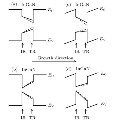
Fig.1. Energy band schematic diagrams of InGaN/GaN QW at zero forward bias for both samples, without((a)for SA and(b)for SB)and with((c)for SA and (d) for SB) considering polarization field. Dashed and solid lines represent energy band schematic diagrams,without and with considering In volatilization,respectively. IR and TR represent the initial region and terminal region of the well layer,respectively.
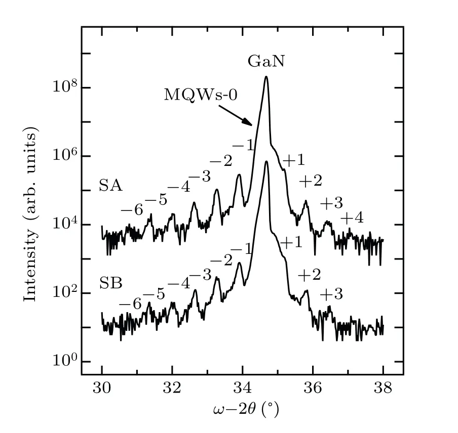
Fig.2. HRXRD ω-2θ scan on GaN(002)plane of SA and SB.
Figure 2 illustrates the HRXRDω-2θscan in the GaN(002)direction for these two samples. The main peaks located at about 34.7°are attributed to the GaN(002)plane.The satellite peaks are considered to originate from the InGaN/GaN MQWs. In addition, by comparison, the satellite peaks are sharper for SA than for SB.Figure 3 shows the HRXRD rocking curves along the (002) and (102) reflections for the two samples. As can be seen in Fig.3, the values of full width at half maximum(FWHM)for the HRXRD rocking curves along the(002)and(102)reflections of SA(SB)are 306 arcsec and 369 arcsec(324 arcsec and 396 arcsec), respectively, indicating that the values of FWHM for the HRXRD rocking curves of SA are narrower than those of SB.All the results obtained from Figs. 2 and 3 show that the SA should have sharper interfaces and better crystal quality than SB.[20-22]Furthermore,based on the aforementioned HRXRD data,such as the intensity ratio of the negative MQW satellite peaks to their positive counterparts-related to the ratio of the layer thickness values, the angular position of the MQW peak, and the angular distance between adjacent satellite peaks, both the thickness(well thickness plus barrier thickness)of one period of MQW and the In mole fraction in the WL can be estimated.[23-25]The thickness values of both samples are estimated to beca.12.4 nm, in approximate agreement with that designed; however, surprisingly, the estimated In mole fraction in the WL is larger for SB (ca. 25.0%) than for SA (ca. 22.5%). This can be explained as follows (see Fig. 1): since the terminal region(TR)of the WL in SB contains a smaller number of In atoms than in SA, the TR in SB should undergo less significant volatilization of In than in SA during the waiting period required for warming-up from the end of low-temperature WL growth to the beginning of high-temperature GaN barrier layer growth; at the same time, the TR with low-In-content, of the WL in SB, as a quasi-cap layer, can suppress the volatilization of In in the initial region(IR)with high-In-content during the waiting period.[26,27]These characteristics may result in SB having a higher average In content than SA, which arises mainly from the contribution of the IR with high-In-content of the WL.This results in the QW in SB presenting a more significant TAS band structure(i.e.,it has a deeper TAS potential well) as shown in Fig. 1 (solid lines), and poorer structural integrity (as mentioned above) due to the more significant In content fluctuations.[28,29]
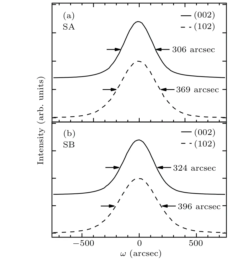
Fig.3. HRXRD rocking curves along(002)and(102)reflections for(a)SA and(b)SB.
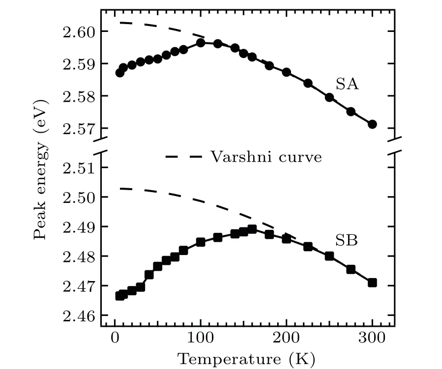
Fig. 4. Curves of temperature-dependent EL peak energy for SA and SB operated at 350 mA.
To explore the transfer and recombination mechanism of the carriers inside the MQWs, figure 4 shows the curve of temperature-dependent EL peak energy of SA and SB at a fixed driving current of 350 mA. As shown in Fig. 4, the temperature-dependent peak energy curves for both the samples present the inverted“V-shape”forms: when the temperature increases,the peak energy first increases,reaching a maximum at a critical temperature due to the thermal broadening effect of the localized carriers, and then decreases due to temperature-induced band gap shrinkage.[30,31]Moreover,it is also found from Fig. 4 that, the temperature behavior of the peak energy exhibits a larger critical temperature(ca. 160 K)for SB than for SA (ca. 100 K); also, the depth of the localized states,which is estimated from the peak energy deviation between experimental data and Varshni’s equation at low temperatures as shown in Fig.4,is larger for SB(36.3 meV)than for SA(15.5 meV).[32,33]The results indicate that the MQWs in SB should have a stronger carrier localization effect than in SA due to the greater potential fluctuation induced by the greater In content fluctuations as mentioned above.
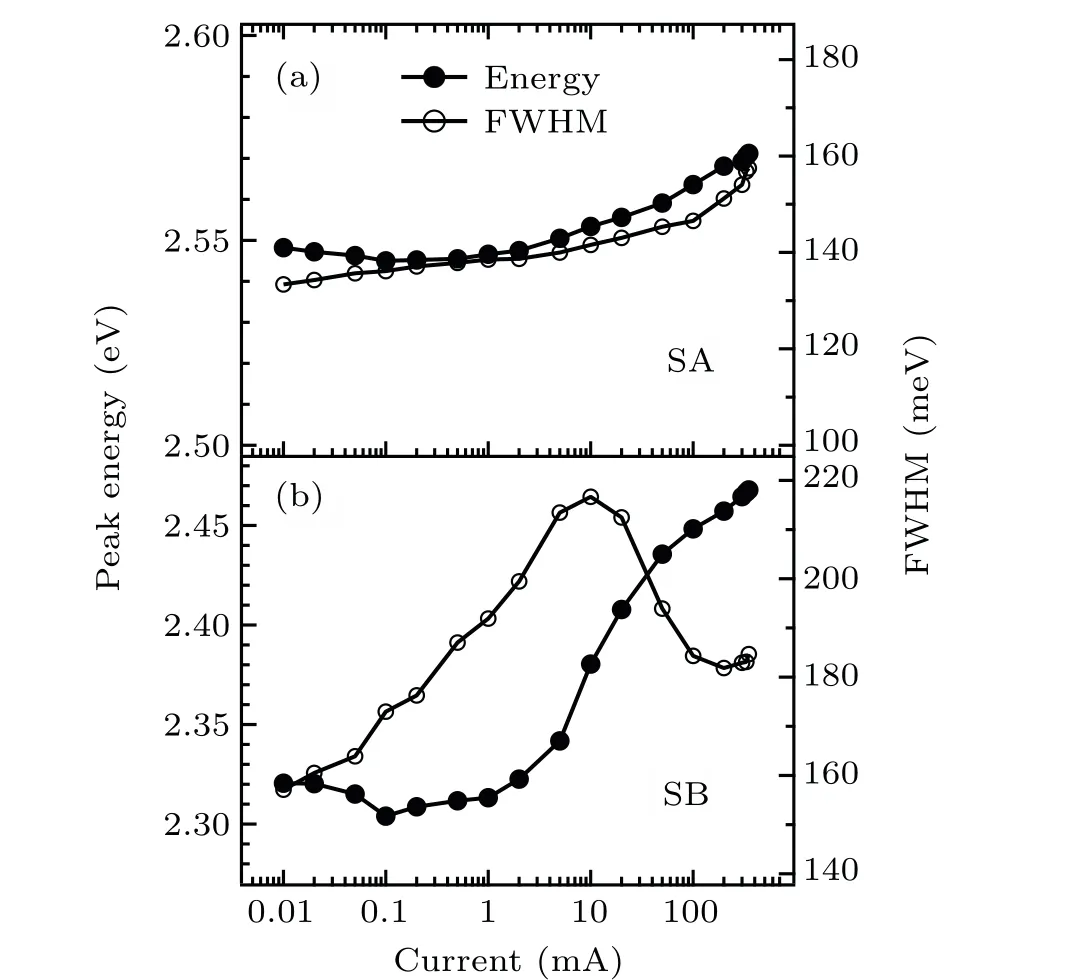
Fig.5. Curves of EL peak energy and FWHM versus driving current for(a)SA and(b)SB at 300 K,respectively.
Figure 5 shows the curves of EL peak energy and FWHM at 300 Kversusdriving current in a current range of 0.01 mA-350 mA for SA and SB. When the driving current increases from 0.01 mA to about 0.1 mA, both SA and SB exhibit a peak red-shift accompanied with an FWHM broadening, but the latter has a larger peak red-shift (16.5 meV) and FWHM broadening(15.88 meV)than their counterparts of the former(3.2 meV and 2.73 meV).This indicates that within the lowest current range and at 300 K,the emission process of the MQWs in both samples is dominated by non-radiative recombination centers thermally activated at a higher temperature of 300 K,[4]but the SB contains more numerous non-radiative centers than the SA because of the poor crystal quality as confirmed by the aforementioned HRXRD measurements; however, when the driving current is further increased from 0.1 mA to 350 mA as shown in Fig.5,the SA exhibits a monotonic increase in both the peak energy and FWHM,which is ascribed to the dominant localized states-related filling effect; by contrast, for SB, the peak energy remarkably shows a monotonic increase, while the FWHM first exhibits a considerable increase in a lower current range(0.1 mA-10 mA)due to the filling effect of the low-energy localized states, then a great decrease in an intermediate current range (10 mA-200 mA)due to the Coulomb screening effect of QCSE, and finally a slight increase in the highest current range exceeding 200 mA due to the onset of the intervention of the high-energy localized states-related filling effect.[34-36]Moreover,for comparison,it should be noted that the significant driving current-dependent Coulomb screening process as observed in SB, is not seen at all in the SA. This will be discussed later.
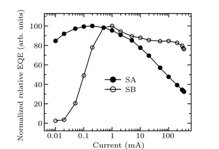
Fig. 6. Curves of normalized relative EQE versus driving current at 300 K for SA and SB.
Figure 6 shows the curves of relative EQEversusdriving current of these two samples, detected at 300 K. When the driving current increases from 0.01 mA to 350 mA, the EQE first increases,reaching a maximum value at the critical current and then exhibits a droop for each of the two samples, implying that the emission processes of the MQWs in both samples are dominated by the non-radiative recombination centers at the lower driving currents,and then by the possible electron leakage or Auger recombination at the higher driving currents.[34,37]Furthermore, it may also be seen from Fig.6 that the SB has a higher critical current(1 mA)than SA(0.2 mA), and as the driving current increases from 0.01 mA to 350 mA,the EQE of SB significantly increases in the lower current range and exhibits a less significant decrease in the higher current range than that of SA.These results reflect the fact that compared with SA,SB exhibits greater non-radiative recombination and a lower efficiency droop: the former can be ascribed to its more numerous non-radiative centers; the latter may be attributed mainly to its less significant electron leakage originating from the deeper TAS potential well of the QW, since the carriers are strongly confined within the IR of the WL as discussed in Figs.1-3,and this prevents them from leaking to the p-GaN side through the barrier-like TR. In addition,the less significant electron leakage for SB may also be due partially to its stronger localization effect as discussed in Fig.4. Furthermore,the significant driving current-dependent Coulomb screening process of SB as shown in Fig. 5, may also compensate partly for the efficiency droop; by contrast,the aforementioned absence of the Coulomb screening process of SA(Fig.5)is believed to be related to its more significant electron leakage,which is consistent with its more significant efficiency droop shown in Fig.6.[38]
4. Conclusions
The structural and optical properties of two different asymmetric triangular InGaN/GaN MQW-based LED samples,in which the In composition in each InGaN WL gradually increases(decreases)for SA(SB)along the growth direction,are investigated by the HRXRD method and the EL method at different driving currents and temperatures. The results show that due to the difference in growth pattern of the WL between these two samples,comparing with the SA,for the SB,the TR of the WL contains fewer In atoms, thus resulting in the less significant volatilization of In ingredient therein;furthermore,this low-In-content TR as a quasi-cap layer, can suppress the volatilization of In ingredient in the high-In-content IR,at the same time,it can also act as a barrier-like layer to prevent electrons from leaking to the p-GaN side. This causes the SB to have a higher In content and a deeper TAS potential well in the QW than SA.It is also consistent with the following measurement results: compared with the SA, the SB has a lower EL peak energy,a stronger structural defect-related non-radiative recombination and carrier localization effect because of the more significant In content fluctuations,and a less significant efficiency droop due to the stronger quantum confinement effect of the carriers inside the more significant TAS potential well. Moreover, the improvement in the efficiency droop for SB may be also attributed partly to its stronger carrier localization effect and Coulomb screening effect.
Acknowledgements
Project supported by the National Natural Science Foundation of China(Grant Nos. 51872167 and 51672163)and the Major Science and Technology Innovation Project of Shandong Province,China(Grant No. 2019JZZY010210).
猜你喜欢
杂志排行

Chinese Physics B的其它文章
- Superconductivity in octagraphene
- Soliton molecules and asymmetric solitons of the extended Lax equation via velocity resonance
- Theoretical study of(e,2e)triple differential cross sections of pyrimidine and tetrahydrofurfuryl alcohol molecules using multi-center distorted-wave method
- Protection of entanglement between two V-atoms in a multi-cavity coupling system
- Semi-quantum private comparison protocol of size relation with d-dimensional GHZ states
- Probing the magnetization switching with in-plane magnetic anisotropy through field-modified magnetoresistance measurement