Perpendicular magnetic anisotropy of Pd/Co2MnSi/NiFe2O4/Pd multilayers on F-mica substrates
2022-01-23QingwangBai白青旺BinGuo郭斌QinYin尹钦andShuyunWang王书运
Qingwang Bai(白青旺), Bin Guo(郭斌), Qin Yin(尹钦), and Shuyun Wang(王书运)
School of Physics and Electronics,Shandong Normal University,Ji’nan 250358,China
Keywords: perpendicular magnetic anisotropy,Co2MnSi,ferrimagnetics NiFe2O4
1. Introduction
Magnetic tunneling junctions (MTJs) with perpendicular magnetic anisotropy (PMA) have high enough thermal stability and low critical switching current in magnetoresistive random access memory (MRAM), so magnetic recording materials with PMA have become one of the research hot spots in recent years.[1-3]Over the years,Co-based multilayer films(Co/Pd and Co/Pt),rare-earth and transition metal alloys(GdFeCo) and L1 ordered alloys (CoPt and FePt) have been studied in depth.[4-6]However, these materials have some limitations such as inadequate chemical or thermal stability and low spin polarizability.[7,8]Full Hessler alloy Co2MnSi(CMS) has a series of advantages, such as good thermal stability, nearly 100% spin polarizability, high Curie temperatureTc(~1000 K), very low Gilbert damping constantα(~0.001), and large tunneling magnetoresistance(TMR).So it has attracted widespread attention from people in recent years.[9,10]CMS is a promising candidate material for magnetic recording.[11-13]
Studies have shown that strong PMA can be induced by the interface effect between ferromagnetic metals (FM)and metal oxides (OX), such as CoFeB/MgO, Co/MgO, and Co2MnSi/NiO structures.[14-16]Moreover,spinel oxides,such as MgAl2O4and MgGa2O4, can further improve the performance of MTJs when used as a tunnel barrier due to their small lattice mismatch with typical FM electrodes.[17,18]NiFe2O4(NFO)is a typical ferromagnetic spinel oxide with high magnetic ordering temperature and high saturation susceptibility. It is a very attractive candidate material for spintronic devices.[19]In particular, NFO has been successfully used as a spin-filtering tunnel barrier with a spin filtering efficiency of up to 22% at low temperatures.[20]Therefore, using NFO as a tunneling barrier for MTJs will increase the electron polarizability and thus increase TMR. Liet al.predicted by theoretical calculation that NFO could induce large PMA.[21]So far, there have been few studies on the PMA of CMS/NFO heterostructures.
In addition, mica substrate has a flat and inert surface, which is very conducive to the epitaxial growth of two-dimensional materials.In recent years, many researchers have grown high-quality thin film materials on mica substrates.[22-24]However, in the field of magnetic thin film materials, there are few studies on preparing of samples on mica substrates. In this paper, the magnetic properties of Pd/CMS/NFO/Pd multilayers deposited on mica substrates by sputtering were compared with those deposited on glass substrates and Si/SiO2substrates.
2. Experiments
All samples in this experiment were deposited on fluorphlogopite mica (F-mica) substrates at 350°C by magnetron sputtering unless otherwise specified. The background vacuum before deposition is better than 6×10⁻⁴Pa. The substrate is rotated at 15 rpm to ensure the uniformity of sputtering deposition. The structure and preparation details of this series of samples are shown in Table 1 (symbols or numbers in parentheses indicate film thickness in nanometers). In this experiment,all NFO layers prepared by sputtering were soon exposed to an oxygen atmosphere of 0.5 Pa for 5 min unless otherwise stated. In this paper,the sputtering rate of each target material is measured by mass weighing method, and the required thickness of film is obtained by controlling the sputtering time. The sputtering parameters of all the targets are shown in Table 2.
The magnetic properties of the samples were measured by an alternating gradient magnetometer AGM:MicroMag 2900.The Hall curve of the samples was measured by four-probe method. The surface morphology of different substrates was measured by atomic force microscopy AFM:BY-5000.
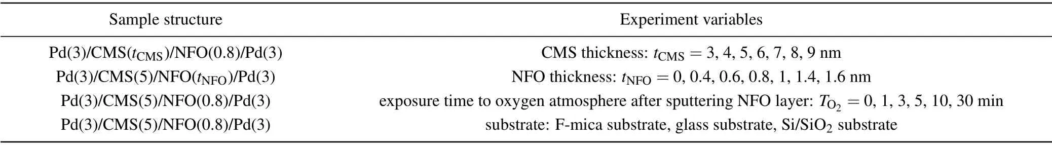
Table 1. Series of samples and corresponding experimental variables.

Table 2. Sputtering parameters for all targets.
3. Results and discussion
3.1. Effects of the thickness of CMS layer on PMA
Figure 1(a) shows the Hall loops of a series of Pd(3)/CMS(tCMS)/NFO(0.8)/Pd(3) multilayers with different CMS thicknesses. Figure 1(b)shows the coercivity field(HC)and Hall resistance(RHall)as functions of the thickness of the CMS layer. WhentCMS=3 nm,the films do not exhibit PMA,because the relatively thin CMS layer cannot form strong interface effect with Pd and NFO to overcome the demagnetization energy.[25]The squareness of Hall loops becomes better andRHallincreases with the increase of CMS thickness. The close to 1 of squareness and largeRHallwere observed at thetCMS=5 nm,indicating that the sample has a strong PMA.As the thickness of CMS continues to increase,the demagnetization energy of the sample increases,so that theRHalldecreases gradually. WhentCMS=9 nm, the PMA is disappear, which is attributed to the interfacial anisotropy energy cannot overcome the demagnetization energy.[15,16]HCof the samples decreases slightly with the increase of CMS thickness,which can be found in Fig.1(b).
Figure 1(c)show the in-plane and out-of-plane hysteresis loops of Pd(3)/CMS(5)/NFO(0.8)/Pd(3).A typical square outof-plane hysteresis loop is observed, with 100% remanence,and a coercive field of about 425.36 Oe(1 Oe=79.5775 A/m).These data are basically consistent with those of Hall loops.The magnetic anisotropy energy density (Keff) value can be estimated from the area difference between the magnetization curve of the in-plane and that of out-of-plane:Keff=∫[M⊥-M‖]dH, whereM⊥is the out-of-plane magnetization,M‖is the in-plane magnetization. The sampleKeffvalue of 0.6711 Merg/cm3was calculated, reflecting the excellent PMA performance of the sample.[14]
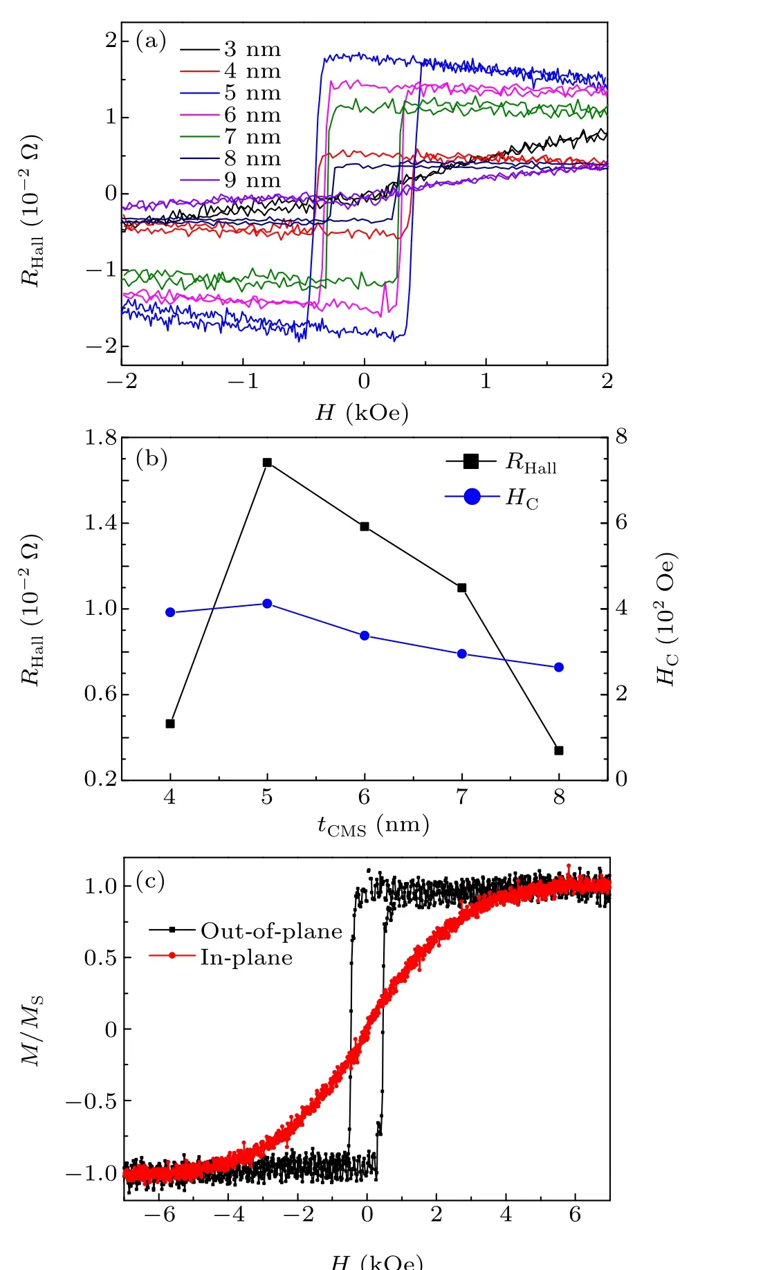
Fig.1. (a)Hall loops of Pd(3)/CMS(tCMS)/NFO(0.8)/Pd(3)under different tCMS,(b)tCMS dependencies of RHall (black)and HC (blue),(c)in-plane and out-of-plane hysteresis loops of Pd(3)/CMS(5)/NFO(0.8)/Pd(3).
3.2. Effect of NFO thickness on PMA
Hall loops of a series of Pd(3)/CMS(5)/NFO(tNFO)/Pd(3)multilayers with different NFO thicknesses are shown in Fig. 2(a).In general, the PMA of FM/OX multilayers is strongly affected by the degree of oxidation at the interface.[26,27]The thickness of the oxide layer is a key factor affecting the oxidation state of the interface, so appropriate oxide layer thickness is crucial for obtaining strong PMA.[14-16,28]WhentNFO=0.2 nm or 1.4 nm,the CMS/NFO interface was in the state of under-oxidation and overoxidation, respectively, the sample is displayed in-plane magnetic easy axis. WhentNFO=0.8 nm,the sample has excellent Hall loops squareness and largeRHall,which reflects the sample has strong PMA. ThetNFOdependence ofHCandRHallwere basically consistent as observed in Fig.2(b),suggesting that theHCof the sample with strong PMA was relatively large only under the change oftNFO. Similar phenomena have been observed in CMS/MgO, CMS/MAO and other structures.[28,29]In conclusion, when the thickness of NFO layer was 0.8 nm,the optimal interfacial oxidation degree of FM/OX interface was obtained,and PMA of the sample is the strongest.
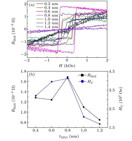
Fig.2. (a)Hall loops for Pd(3)/CMS(5)/NFO(tNFO)/Pd(3)with various tNFO from 0.2 nm to 1.4 nm,(b)RHall (black)and HC (blue)dependence on tNFO.
3.3. Effect of TO2 on PMA
It is well known that PMA is mainly originated from the orbital hybridization of Co-3d and O-2p at the interface of CMS/OX multilayers.[29,30]During the preparation of oxide layer, a certain proportion of O2is usually injected into the sputtering gas in order to reduce oxygen loss and oxygen vacancy in the oxide layer.[14-16]However,the ferromagnetic layer will be overoxidized if too much oxygen is introduced. Therefore, in this experiment, the oxide layer was sputtered in high purity Ar environment,and then exposed to high purity O2atmosphere, so that the sputtered oxide layer was sufficient oxidized to eliminate oxygen loss and oxygen vacancy. Figure 3(a) shows the Hall loops of a series of Pd(3)/CMS(5)/NFO(0.8)/Pd(3)multilayers with differentTO2(exposure time to oxygen atmosphere after sputtering NFO layer). Figure 3(b) shows theRHallandHCdependence ofTO2. WhenTO2=0 min,the Hall loops squareness is poor andRHallis small,indicating that the PMA of the sample is weak.This is because the oxygen loss and the oxygen vacancy in the NFO lead to insufficient Co-O orbital hybridization at the CMS/NFO interface,which resulting in a weak interface effect of CMS/NFO.[17,31]The close to 1 of squareness and largeRHallcan be observed at theTO2≥5 min, showing that the sample exhibited strong PMA. TheRHallandHCof the sample remain basically unchanged asTO2continues to increase.To sum up, oxygen loss and oxygen vacancy in NFO can be basically eliminated atTO2≥5 min,and no overoxidation will occur at the CMS/NOF interface.
Fig. 3. (a) Hall loops for Pd(3)/CMS(5)/NFO(0.8)/Pd(3) with various TO2 from 0 min to 30 min,(b)RHall (black)and HC (blue)dependence on TO2.
3.4. Effect of substrates on PMA
The Hall loops and the in-plane and the out-of-plane hysteresis loops of a series of Pd(3)/CMS(5)/NFO(0.8)/Pd(3)multilayers deposited on different substrates are shown in Fig. 4. The samples deposited on F-mica substrates have largerRHallandHCcompared with those deposited on glass and Si/SiO2substrates. SuitableHCcan make the magnetic properties of thin films more stable and facilitate the miniaturization of devices.[32]By calculating theKeffvalue of these samples, it was found that theKeffvalue of the sample deposited on the F-mica substrate is 0.6711 Merg/cm3, which was about 30% larger than that of the samples deposited on the glass (0.475 Merg/cm3) and Si/SiO2(0.511 Merg/cm3)substrate. The surface morphologies of three different substrates were observed by AFM, as shown in Fig. 5. As can be seen from the figure, F-mica substrate has a flatter surface than glass and Si/SiO2substrate. The roughness of F-mica substrate is 0.083 nm,which is only one third of that of glass substrate (0.231 nm) or Si/SiO2substrate (0.243 nm). The flatness of the substrate provides conditions for the deposition of high quality films and interfaces on it, which is more conducive to improving the PMA of multilayers.[22-24,33]
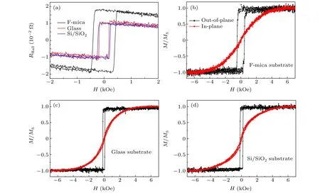
Fig. 4. (a) Hall loops and (b)-(d) in-plane and out-plane M-H loops of Pd(3)/CMS(5)/NFO(0.8)/Pd(3) multilayers deposited on different substrates.
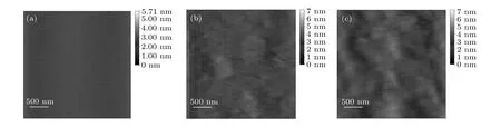
Fig.5. Surface morphologies of(a)F-mica substrates,(b)glass substrates,and(c)Si/SiO2 substrates.
4. Conclusion
A series of Pd(3)/CMS(tCMS)/NFO(tNFO)/Pd(3)multilayers were fabricated on F-mica substrates by magnetron sputtering. The Pd(3)/CMS(5)/NFO(0.8)/Pd(3) multilayer structure with the best PMA performance was obtained by adjusting the thickness of CMS and NFO,and the sampleKeffvalue was 0.6711 Merg/cm3. In this study,the NFO layer fabricated by sputtering in high purity Ar environment was exposed to high purity O2atmosphere for 5 min,which could effectively eliminate the oxygen loss and oxygen vacancy in NFO,ensuring enough Co-O orbital hybridization at the CMS/NFO interface, and thus effectively improve the sample PMA. Compared with the samples deposited on glass and Si/SiO2substrates, the multilayers deposited on F-mica substrates have largerRHallandHC,and theKeffvalue is also significantly increased. TheKeffvalue of the Pd/CMS/NFO/Pd multilayers deposited on the F-mica substrate is 0.6711 Merg/cm3,which is about 30%larger than that of the samples deposited on the glass (0.475 Merg/cm3) and Si/SiO2(0.511 Merg/cm3) substrates. In the following work,we will try to applying a magnetic field during the film deposition to continue to enhance the PMA of the multilayers.[34]
Acknowledgment
Project supported by the Shandong Provincial Natural Science Foundation,China(Grant No.ZR2018MEM004).
杂志排行

Chinese Physics B的其它文章
- Superconductivity in octagraphene
- Soliton molecules and asymmetric solitons of the extended Lax equation via velocity resonance
- Theoretical study of(e,2e)triple differential cross sections of pyrimidine and tetrahydrofurfuryl alcohol molecules using multi-center distorted-wave method
- Protection of entanglement between two V-atoms in a multi-cavity coupling system
- Semi-quantum private comparison protocol of size relation with d-dimensional GHZ states
- Probing the magnetization switching with in-plane magnetic anisotropy through field-modified magnetoresistance measurement