Study on a novel vertical enhancement-mode Ga2O3 MOSFET with FINFET structure
2022-01-23LiangliangGuo郭亮良YumingZhang张玉明SuzhenLuan栾苏珍RundiQiao乔润迪andRenxuJia贾仁需
Liangliang Guo(郭亮良) Yuming Zhang(张玉明) Suzhen Luan(栾苏珍)Rundi Qiao(乔润迪) and Renxu Jia(贾仁需)
1The Key Laboratory of Wide Band Gap Semiconductor Materials and Devices,School of Microelectronics,Xidian University,Xi’an 710071,China
2Xi’an University of Science and Technology,Xi’an 710000,China
Keywords: gallium oxide,E-mode,device simulation,threshold voltage
1. Introduction
The monoclinicβ-phase of gallium oxide(Ga2O3)is one of the promising ultra-wide bandgap (UWBG) materials for power device application due to its fundamental properties and a low-cost manufacturable native substrate,[1,2]such as large bandgapEgof~4.9 eV,critical electric fieldEcof 8 MV/cm,and electron saturation velocityυsatof 1.8×107cm/s-2.0×107cm/s. In recent years, the research on Ga2O3metaloxide-semiconductor field-effect transistor (MOSFET) devices is more in-depth worldwide,[4-12]such as Ga2O3vertical MOSFET withVbr>1 kV is published.[12]Ga2O3MOSFET is becoming a major breakthrough in the research of high temperature, voltage, and power devices. Due to the low donor energy level (Ec-0.04 eV) formed by the oxygen vacancy in the growth process, theβ-Ga2O3is an ntype semiconductor. However, due to the large hole effective mass and the self-trapping effect, the p-type doping of Ga2O3has not achieved adequate practical progress so far.[3]The research of Ga2O3based MOSFET devices mainly focuses on the depletion-mode(D-mode),[4-7]and the more indepth studies of enhancement-mode (E-mode) MOSFET are urgently pending.[8-10]Because the MOSFET worked in enhanced mode operation withVth>0 V is considered to work as a preferred safety mode.[11,12]
Technology-Computer-Aided-Design(TCAD)provides a practical approach to understand the device physics. Up to now, there have been many works on the TCAD simulation ofβ-Ga2O3transistors, especially in the vertical MOSFET.[13-21]Researchers have gained comprehensive knowledge of the material characteristics of Ga2O3single crystal and significantly promoted the incomplete ionization model, mobility model, energy band model, collision ionization model, high field mobility model, temperature dependence model of gallium oxide for practical device simulation.The simulation work of the Ga2O3device currently remains on the change of characteristic regularity and trend,thus lacking the capability to precisely quantify the electrical parameters of the device, such as the breakdown voltage (Vbr), the maximum electric field strength, the output, and the transfer characteristics of the device. The vast deviations regarding the device performances between the simulation and the experiments are critical issues hindering Ga2O3device design and broader applications.[22,23]
This paper reports establishing the basic model of vertical E-mode Ga2O3MOSFET by TCAD and demonstrating the model’s correctness by combining it with the experimental data. Experimental data verify the correctness of the model,and the device structure is optimized considering the output current and threshold voltage.
2. Simulation details
2.1. Bandgap model
The bandgap (Eg) of Ga2O3is set as 4.85 eV at room temperature. According to the equation,[24]the relationship betweenEgand the lattice temperature(T)is as follows:

whereTis the lattice temperature, dEg/dT= 4.45×10³(eV/K),βis 2000 K.
2.2. Effect of incomplete ionization and compensation doping
Since the incomplete ionization and compensation doping have a significant influence on the electrical properties of Ga2O3devices,especially in the drift region,the model of the incomplete ionization state of donor energy level is established as follows:[19]
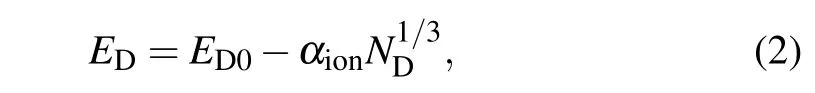
whereED0is the zero doping ionization energy, which is 36.3 meV,αionis 2.0609×10⁻⁸eV·cm (effective electronic mass is 0.28m0,and the effective density of states(NC)of the local conduction band is 3.67×1018cm-3).[20]
2.3. Mobility model
For power Ga2O3MOSFET, mobility is one of the essential electrical parameters, and modeling usually considers factors such as the doping concentration,the high field saturation effect,and the surface effect. Because electrons flow in a vertical MOSFET’s fin center,the surface effect does not play an important role. The low electric field mobility of Ga2O3is usually used as follows:[21]
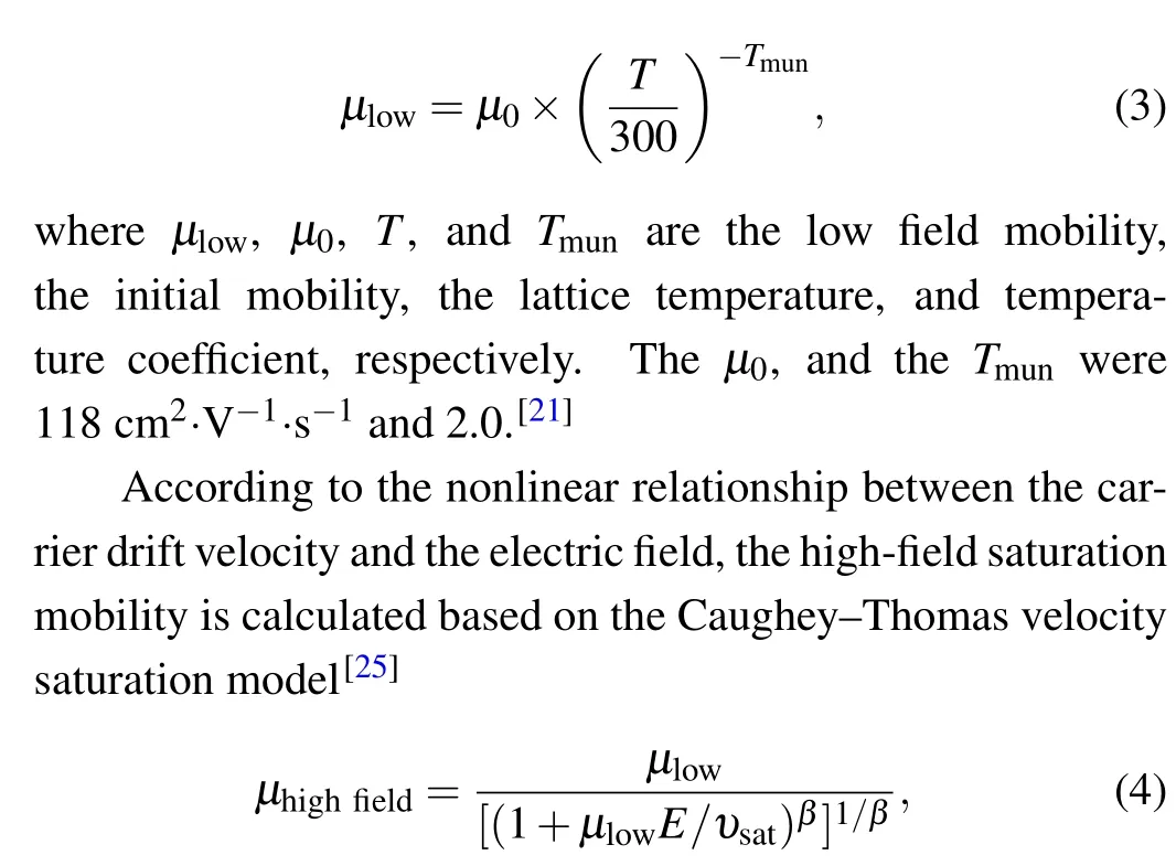
whereυsatis the saturation drift velocity of the carrier andEis the electric field. Because the [001] direction is the preferred direction for fabricatingβ-Ga2O3vertical MOSFETs,the optimization of stimulation parameters is conducted only along thezdirection,corresponding to[001]orientation.The carrier saturation drift velocityυsatin Ga2O3is about 1.708×107cm/s.[26]The formula of parametersβare the same as that of the Siβ(T)relationship,as follows:[5]

whereAmin,Ad,AN, andA*are parameters related to Ga2O3materials.[16]
2.4. Device structure
The simulated structure and related parameters of the vertical Ga2O3MOSFET is shown in Fig.1 and Table 1.
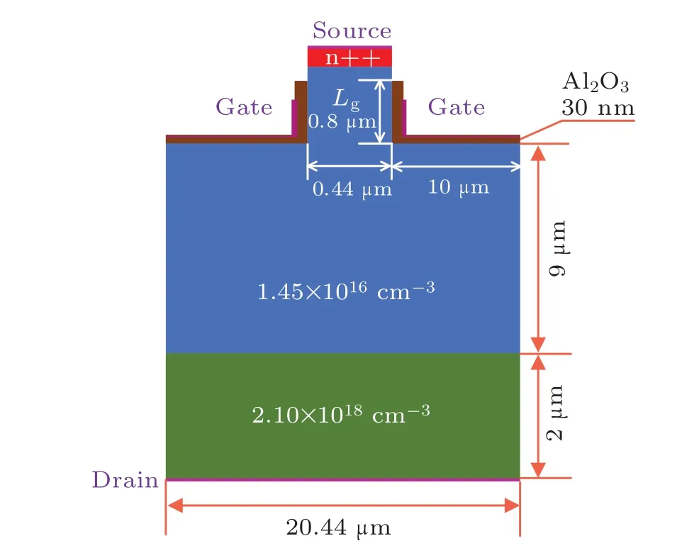
Fig.1. Structure of vertical gallium oxide MOSFET.The green area is drain area,the blue area is epilayer film,the red area is source area.
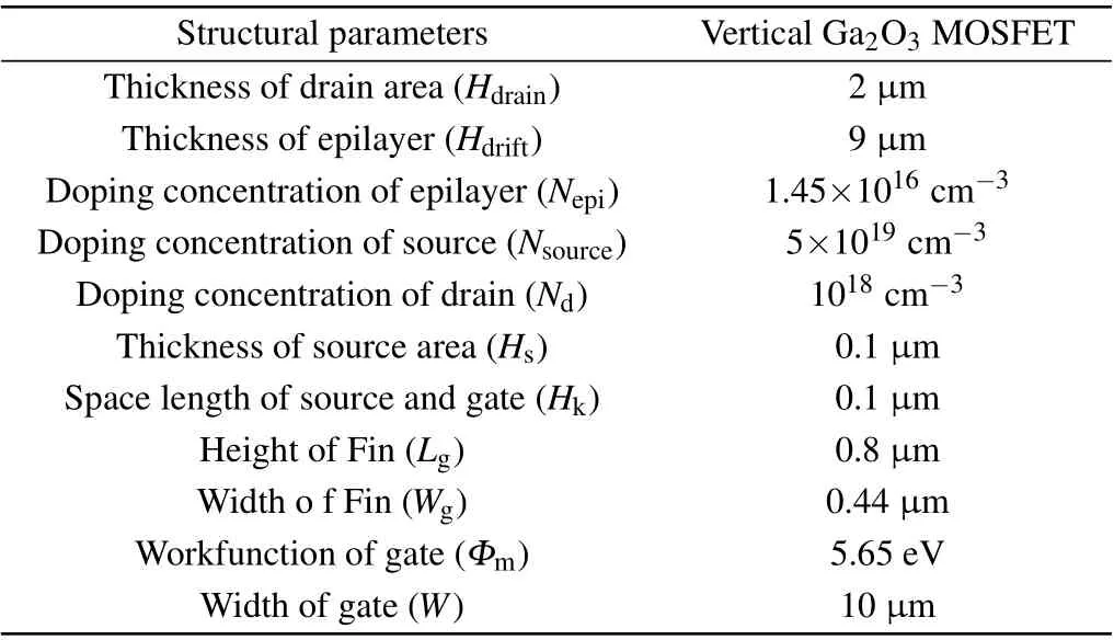
Table 1. Structural parameters of the vertical Ga2O3 MOSFET.
3. Results and discussion
Figure 2 shows the transfer curve and the output curve obtained by TCAD,whcih are consistent with the experimental results.[23]In Fig. 2(a), the threshold voltage (Vth) obtained is 0.24 V (Vthis defined as the gate voltage whenIds= 0.1 mA/cm2). In Fig. 2(b), theIdsis microampere level when the gate voltage is less than 0 V.Idsin the saturation region and theIdswith TCAD are 22.7% and 6.9%smaller than the literature values, respectively.[23]This is becauseµ0=118 cm2·V-1·s-1used in the Arora model comes from practical measurement,which is not particular optimized for simulation. We note that the output saturation current of the device will increase with increasingµ0,and the simulation results and experimental can reach better consistency.
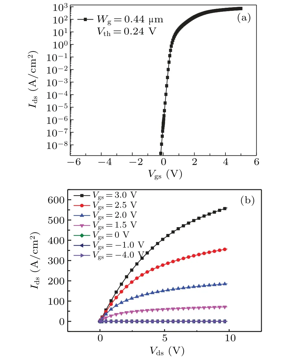
Fig. 2. (a) Transfer characteristics and (b) output characteristics of vertical Ga2O3 MOSFET.
Figure 3 shows the output and transfer characteristic curve of different gate metals with different work functions. It shows that the output current density decreases,and the threshold voltage increases with the increasing of work function. As the metal work function is rising up to 5.95 eV, the device operation will change from depletion device to enhancement device. In order to realize the E-mode MOSFET device, the material with a large gate metal work function should be chosen,such as Au and Pt for Ga2O3devices.
Figure 4 shows the output and the characteristic transfer curves with different gate oxide materials under the oxide layer thickness(HO)is 30 nm. TheIdsof the device with the HfO2layer increases with the increase of the dielectric constant of the gate oxide material. The threshold voltage reaches the maximum whenIdsandVthwith SiO2layer are the minimums at the same thickness, which is attribute toIdsandVthincreasing with the increase of the oxide layer’s dielectric constant(εox).

Fig.3. (a)Output curves and(b)transfer characteristic curves of the device with different metal work functions.
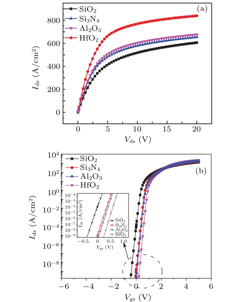
Fig.4. (a)Output curves and(b)transfer characteristic curves of the device with different gate oxide materials.
Figure 5 shows the output and transfer characteristic curves with different epilayer concentrations(Ndrift). The output current density increases, and the threshold voltage decreases with the increase of epitaxial layer concentration.With the increase of epitaxial layer concentration,the hole concentration in the depletion region of the device channel becomes smaller and easier to be turned on under the same gate metal condition so that the threshold voltage will shift to the left.The results indicate that the epitaxial layer concentration should not exceed 5×1016cm-3.
Figure 6(a) shows the transfer characteristic curve of channel height(Lg)at different channel heights. It can be seen from the curves that the output current density decreases,and the threshold voltage increases with the increase of channel height. The resistance in the channel region increases with the increase ofLg,leading to the current decreasing and the threshold voltages shift to the right,as shown in Fig.6(b). With the increase of channel height, the increase of threshold voltage decreases gradually, and the output current decreases significantly, suggesting that the channel height should be smaller than 1.5µm.
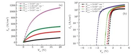
Fig.5. (a)Output curves and(b)transfer characteristic curves of the device with different epilayer concentrations.
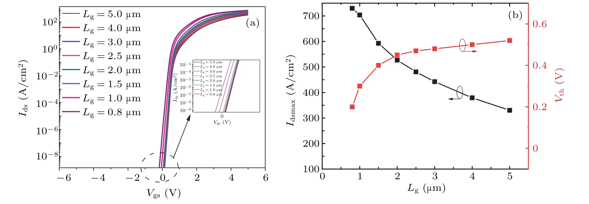
Fig.6. (a)Transfer curves and(b)characteristics comparison at different channel heights.
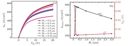
Fig.7. (a)Transfer curves and(b)characteristics comparison at different source heights.
Figure 7(a)shows the output curves with different heights of the source region (Hs). It can be seen from Fig. 7(b) that with the increase of the source height,the output current density increases firstly and then decreases. Threshold voltage firstly decreases and then increases. With the increase of the source height, the depletion of the channel undermines, and the current density increases. When the source thickness is more than 0.2 µm, theLgand the resistance become rising,and the current decreases. The device’s threshold voltage is mainly related to the concentration and width of gate metal and channel area. Therefore, the source area thickness of the device is set at 0.1µm-0.3µm is more suitable.
Figure 8 shows the output transfer characteristic curves with different oxide layer heights (HO). It can be seen from the curves that with the increase of oxide layer height,the output current density first decreases and then increases. Due to the work function difference between the gate metal and the semiconductor, the device’s channel is in the depletion state,and the device is turned off. When the thickness of the gate oxide layer is reduced,the gate voltage is easier to control the formation of holes,and the depletion region is easier to form,leading to an increase of the threshold voltage of the device.When the device is turned on,the output current increases with decreasing the oxide layer’s height. When the thickness of the oxide layer is beyond 0.13µm,the threshold voltage becomes negative. Therefore, the oxide thickness of the device should not exceed 0.08µm.
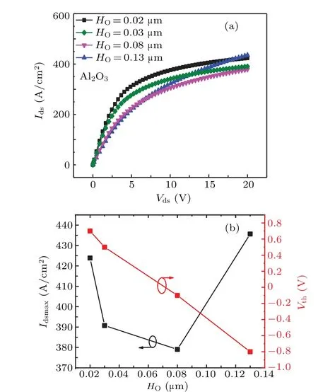
Fig.8. (a)Out curves and(b)characteristics comparison with different oxide layer heights.
Figure 9 shows the output and transfer characteristics of different channel widths(Wg). The output current density and the threshold voltage decrease with the increase of channel width. The cross-sectional area of current flow increases,and the resistance of channel area decreases with the increase of channel width at the same channel length so that the output current will increase with the increase of channel width.At the same gate voltage, the resistance in the channel region of the device becomes smaller and easier to turn on,and the threshold voltage will shift to the left.
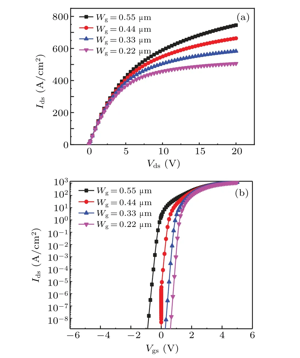
Fig. 9. (a) Output curves and (b) transfer characteristic curve of the device with different drift heights.
Through simulation above,it can be found that the width and height of source“fin”will have a significant impact on the performance of the device. Therefore,the high precision etching process is the key step to achieve this device. In addition,the covering ability of the gate electrode on the“fin”mesa also has influence on the gate control of the device.
4. Conclusion
Based in TCAD simulation and experimental data verification, we propose an improved Ga2O3model for Ga2O3MOSFET device simulations.Based on the established model,the static characteristics of vertical Ga2O3MOSFET are calculated by the TCAD simulation software. The simulation results are in good agreement with the experimental results giving rise to optimization simulation parameters of the device. Through the optimization of the gate metal work function, the channel length, the width, the gate oxide material,the thickness, the epitaxial layer concentration thickness, the source region thickness,the concentration are included in the simulation. We found that the gate metal material, the oxide layer thickness and material,the source region concentration,the epitaxial layer concentration, the source region thickness,and the source region concentration are the key factors. The channel region’s width and height greatly influence the output current,while the gate metal material,the thickness of the oxide layer,and the concentration of material and epitaxial layer greatly influence the threshold voltage. According to the simulation results,materials with a large gate metal work function and large oxide dielectric constant should be chosen for fabricating the E-mode MOSFET device. The epitaxial layer concentration should not exceed 5×1016cm-3, and the channel height of the device should be smaller than 1.5µm. The thickness of the source area is set at 0.1µm-0.3µm. The thickness of the oxide layer should be less than 0.08 µm. Our findings from the theoretical calculations are omportant guidelines in designing and manufacturing the Ga2O3MOSFET device.
Acknowledgements
Project supported by the National Natural Science Foundation of China (Grant Nos. 61974119, 51602241, and 61834005), the Natural Science Foundation of Shannxi Province, China (Grant No. 2020JM-532), and the Science Foundation of Xi’an University of Science and Technology(Grant No.2018QDJ036).
杂志排行

Chinese Physics B的其它文章
- Superconductivity in octagraphene
- Soliton molecules and asymmetric solitons of the extended Lax equation via velocity resonance
- Theoretical study of(e,2e)triple differential cross sections of pyrimidine and tetrahydrofurfuryl alcohol molecules using multi-center distorted-wave method
- Protection of entanglement between two V-atoms in a multi-cavity coupling system
- Semi-quantum private comparison protocol of size relation with d-dimensional GHZ states
- Probing the magnetization switching with in-plane magnetic anisotropy through field-modified magnetoresistance measurement