Light focusing in linear arranged symmetric nanoparticle trimer on metal film system
2022-01-23YuxiaTang唐裕霞ShuxiaWang王蜀霞YingzhouHuang黄映洲andYuruiFang方蔚瑞
Yuxia Tang(唐裕霞) Shuxia Wang(王蜀霞) Yingzhou Huang(黄映洲) and Yurui Fang(方蔚瑞)
1State Key Laboratory of Coal Mine Disaster Dynamics and Control and Chongqing Key Laboratory of Soft Condensed Matter Physics and Smart Materials,College of Physics,Chongqing University,Chongqing 400044,China
2Applied Physics,School of Computer Science and Information Engineering,Chongqing Technology and Business University,Chongqing 400067,China
3Key Laboratory of Materials Modification by Laser,Electron,and Ion Beams(Ministry of Education),School of Physics,Dalian University of Technology,Dalian 116024,China
Keywords: electric field enhancement, light focusing, nanoparticle trimer on metal film system, plasmonic hybridization
1. Introduction
Over the past decades, metal nanostructures have attracted researchers’ tremendous interest because of their amazing ability to confine light in subwavelength regions.This ability is induced by the collective oscillation of free electrons on metal nanostructure surface called surface plasmon.[1-3]When the light excited oscillation reaches resonance at suitable frequency, the extremely enhanced electromagnetic field could be generated on metal surface, which is called localized surface plasmon resonance (LSPR). LSPR has tremendous applications in various research fields, such as surface-enhanced Raman scattering (SERS),[4-7]nonlinear optics,[8,9]sensing,[10,11]surface catalysis,[12,13]solar cells,[14,15]plasmon waveguide,[16,17]and so forth.
The electromagnetic enhancement in metal nanostructures is strongly influenced by their size,shape,arrangement,composition, and ambient environment. Lots of structures have been investigated to explore the interesting applications in the past.[1,11,17]In these structures, metal nanoparticles(NPs)on metal film system exhibits unique surface-enhanced phenomenon, in which electromagnetic field would be redistributed and light is confined not only between NPs and NPs but also between NPs and metal films. One or more hot spots will be generated in such a system.This is apparently different from the metal nanoparticle alone or the NPs on the dielectric film system.[18-22]Furthermore, our latest work pointed out the heterodimer on metal film could induce energy focusing at the bottom of small nanoparticle(NP)on film, and the energy between small NP and the film can be more than 5 times stronger than that between the larger NP and film in this structure.[19]Such a structure has potential applications in SERS,ultra-sensing,surface catalysis. In these reports,the results show that electromagnetic field redistribution comes from the strong coupling between particle surface charges and induced image charges on metal film. Therefore, both the wavelength of incident light and the particles size or arrangement of NPs play important roles in this novel phenomenon.
In this work, optical properties of linear arranged symmetric Ag NPs trimer on Au film (trimer-film) system are investigated with finite element method (FEM). The electric field and surface charge distributions are firstly investigated under 633-nm light illumination in the systems with various particle sizes. It is not difficult to find that the light energy on film is mainly confined at bottoms of side NPs not the middle one in the system. This conclusion has no relationship to the size ratio of NPs in trimer-film system,which is quite different from the dimer on metal film system that the light energy is always confined at the bottom of smaller NP.[19]And then,the influence of wavelength and particle size on light confinement in this system is also investigated.
2. Simulation methods
All systems in this work were numerically investigated in three-dimensional(3D)space using the finite element method(COMSOL4.3a commercial package).Our trimer-film system is consisted of three Ag nanospheres located in 1 nm above the gold film with 100-nm thickness. The three Ag NPs with different diameters are arranged linearly which are similar to our latest work.[19]The diameters of middle Ag NP in different systems would be changed in this work. The diameters of two side Ag NPs are always the same. The trimer is surrounded by air. The gaps between each two adjacent particles in the trimer are 1 nm. When the intervals between the nanoparticles and nanoparticles,and between the nanoparticles and the metal film are 1 nm, the near-field interaction between NPs and NPs and NPs and film becomes very strong.[23-26]In the main text analysis, the gap size is chosen as 1 nm because it is a very typical thickness for monolayer of molecules adsorbing on particles. The main purpose of the work is to provide reference theoretical results to experiments that the molecules adsorbing on particles for sensing. The trimer-film system was excited with light at polarization along linear trimer axis,coming from the trimer side normal to the Au film. The electric field amplitude of incident light is set as 1 V/m. The simulation domain is a cylinder with a 2000-nm diameter. The upper part of the simulation cylinder is air domain with 1000-nm height. The trimer is in this domain. The bottom of the air domain is Au film with 100-nm thickness. The Au film is a cylinder slab on glass substrate and extended to the perfect matched layer(PML).Non-uniform meshes were used to format the object. In particular, the mesh of nanoparticles is super fine. The smallest size of the surface and the body of Ag particles are set respectively as 0.52 nm and 1 nm. The mesh of Au film is extra fine and the smallest size is 1 nm.The largest mesh was set to less thanλ/6(λis the wavelength of incident light). Scattering boundary condition and PMLs(300 nm)are used to reduce the boundary scattering. The relative permittivity of Au/Ag is extracted from the experimental data of Johnson and Christy.[27]
3. Results and discussion
3.1. Electric field enhancement distribution of trimer–film system
Firstly, the electric field distribution of three different trimer-film systems under 633-nm light illumination is investigated and the results are shown in Fig. 1. The diameters of the middle NP in three systems are 40 nm,80 nm,and 120 nm,respectively. The diameters of side NPs remain 80 nm. For convenience,the three systems are labeled respectively as 80-40-80, 80-80-80, and 80-120-80 in the following discussion.Just as one expected, we could find the electric field in the side NP-film gaps(L)are hugely enhanced in Figs.1(a)-1(c),and which are even larger than that in NP-NP gaps(P).The result is accordance with previous work on dimer system.[18,21]However, it is interesting that the electric field enhancement in middle NP-film gap(M)is very small compared with that in the gaps L and P in all the three systems. This means the light energy is highly focused on the gaps between the sides NPs and the metal film. Figures 1(d)-1(f)display the electromagnetic energy density distributions in the three systems,resulting in more energy confined in the side NP-film gaps. The results are quite different from the heterodimer on metal film system that the light is focused on the smaller nanoparticle.[19]To obtain a further understanding about this phenomenon,the electric field enhancement in different gaps, which is defined as|E|/|E0|, illustrated as inset histograms in Figs.1(a)-1(c),
where|E| is the maximum value of the electric field in localized electric fields in Figs. 1(a)-1(c) and|E0| is the incident field value. For the homogenous 80-80-80 system, the enhancements in the gaps L and P for 633 nm are about 540 and 219,respectively. The ration of the electric field enhancement of the two gaps is more than 2.46. The difference would bring about 36.6 times larger in SERS enhancement in the gap between NPs and metal film compared to the gap between NPs and NPs, which is similar to the dimer on film system.[21]However, electric field enhancement in the gap M (less than 14) is the almost one thirty-eighth of the enhancement in the gap L. In the gap L, the light power and the SERS enhancement factor respectively are about 1444 times and 2.2×10⁶times larger than that in the gap M, which displays a much great light focus on film and means the light signal for the middle NP can be neglected in the trimer. At meanwhile,from the data in Fig. 1, one could clearly see that light focusing ability on film gets stronger with the diameter of middle NP increasing. When the diameter of the middle NP is 120 nm the ratio of electric field enhancement in the gap L(668)to P(183)could achieve more than 3.65. Furthermore,there is an obvious increase for the electric field enhancement in the gap L and a decrease for that in the gap P as shown in Fig. 1(c),which demonstrates the stronger light focus ability obtained in the 80-120-80 system.
For better understanding the formation of the interesting light focusing phenomenon, the distributions of surface charges on the NPs and induced image charges on the film surface are illustrated in Figs. 1(g)-1(f). Taking the case of the 80-80-80 system in Fig.1(g)as an example,a large amount of surface charges gathered near the gaps between NPs and NPs.Every NP is equivalent to a dipole,which is illustrated by the red solid arrows in Fig. 1(g). The coupling between dipoles and dipoles would result in a strong near-field enhancement.The trimer could be considered as a large dipole because of the coupling between NPs and NPs.At the same time,because of the result of electrostatic effect,the induced image charges in metal film formed three dipoles,as indicated by black solid arrows,which also could be equivalent to an imaging-induced opposite dipole on the film. From the dipoles’ orientations,when the dipoles corresponding to NPs coupled with dipoles in the film, the effect is equivalent to the case that effective dipoles coupled in the direction normal to the surface, which is illustrated by the black dashed arrows. One should find that the two side dipoles are tilted in a large angle. There exists the strongest electric field enhancement in the gap L.The middle dipole is too small which results in an extremely weak nearfield enhancement in the gap M.It is obvious that the similar situation of the dipole coupling can be observed between NPs and NPs and between NPs and metal film in the other two systems,as shown in Figs.1(h)-1(l). This result confirms our previous conclusion that the light is confined in the interval between side nanoparticle and Au film no matter what diameter of the middle nanoparticle is.

Fig.1. Electric field and surface charge distributions of three trimer-film systems. (a)-(c)The electric field distributions of three different Ag trimers on a 100-nm thick Au film with a 1-nm gap at 633 nm. The diameter of the side Ag nanoparticles(NPs)both are 80 nm in the trimers. The diameter of the middle one(marked as d)is(a)d=80 nm, (b)d=40 nm, and(c)d=120 nm. The insets are the values of electric enhancement at the gaps indicated as L,M,and P.The red and black arrows respectively represent the directions of the incident wave vector k and the polarization in panel(a).(d)-(f)Simulated energy density distributions of the three structures corresponding to panels(a)-(c). Logarithmic scale is used for a good contrast. The red arrows show the power flow direction. (g)-(l)Simulated surface charges distributions in the three systems corresponding to panels(a)-(c). The red arrows in panel (g) show the induced dipoles in the particles. The black arrows show the induced image dipoles in the metal film. The black dashed arrows indicate the effective dipoles.
3.2. Focusing effect of trimer–film system
Since the surface plasmon is great influenced by the wavelength of the incident light,light focusing in trimer-film depending on exciting light wavelength is investigated here.Figure 2(a) shows the electric field distribution of the trimer on 100-nm-thick Au film with 1-nm gap,in which the particle diameters are 80 nm,40 nm,and 80 nm,respectively. The excitation light wavelengths are 532 nm, 555 nm, 633 nm, and 705 nm,respectively. Among these wavelengths,532 nm and 633 nm are the two most common excitation wavelengths in SERS experiments, and 555 nm and 705 nm are two oscillation wavelengths. From the electric field distribution,it is obvious that the light focusing phenomenon is greatly influenced by the wavelength of the incident light. When the system is excited by 532-nm light,the energy is mainly confined in the gap P(between two nanoparticles). While the energy confined in the gap L (between NPs and metal film) is more than that in the gap P for 633-nm light. For 555-nm light and 705-nm light, the electric field energies focused on the gap P and the gap L are both strong.
To obtain more information,the absorption spectra of the 80-40-80 system in the visible and near-infrared region are shown in Fig.2(b). The red solid curve represents the absorption of the system in which the thickness of Au film (labeled as“h”)is 100 nm. The green dot curve represents the absorption of 80-40-80 trimer on a glass substrate with 1-nm gap(Au film thicknessh=0 nm). Apparently,the existence of Au film would induce obvious different spectrum shapes. When the Au film thicknessh=100 nm, two resonance peaks appeared at 555 nm (labeled asl′=2) and 705 nm (labeled asl′=1). Compared with no Au film,there is an additional resonant peak (705 nm) at longer wavelength in the trimer-film system, which is the results of effective coupling of surface charges on nanoparticles and induced image charges on metal film surface. The 420-nm absorption peak mostly comes from the contribution of Au film. Figure 2(c) exhibits the electric field enhancement as a function of wavelength in the gaps between NPs and NPs(the blue line for the gap P)and between NPs and metal film (the red line for the gap L and the green line for the gap M). The electric field enhancements reach maximal value nearby the two resonance peaks,which is consistent with the common sense that the light energy is confined greatly at the resonance frequency. The blue, red, and green dot lines in Fig. 2(c) represent respectively the enhancement in the gaps P, L, and M in the case of the trimer on a glass substrate (Au film thicknessh=0 nm). Obviously, without the gold film,the electric field enhancement in gaps L and M is very small compared with that in the presence of gold film.However, for gap P, there is small difference in the electric field enhancement in the absence or presence of Au film for 555 nm, but there is a weak enhancement effect at resonant wavelength 705 nm without Au film.
Furthermore,there are still some interesting results found here. It is easy to find out there is an interesting energy region(595 nm~705 nm) where the enhancement in the gap P is smaller than that in the gap L.When the diameter of the middle nanoparticle increases, the phenomenon becomes more obvious. For the 80-80-80 system, at resonance peak withl′=1 the near-field enhancement in the gap P is stronger than that in the gap L, but the case is just contrary at resonance peak withl′=2(see Figs.S1(a)and S1(b)in supporting information). In the range of 555 nm-740 nm, the enhancement in the gap P is smaller compared to that in the gap L. It covers a wider range of wavelength than the 80-40-40 system. For the 80-40-80 system (as shown in Fig. 2(c)), when the incident light wavelength exceeds a range of 595 nm-705 nm,the enhancement in the gap P is stronger than that in the gap L, especially in the short wavelength range. In above short wavelength range, the trimer-film system shows very weak coupling in the gap L.The near-field enhancement originates mainly from the coupling between NPs and NPs. For the electric field in the interval between NPs and metal film, the location of the enhancement hot spot is relatively stable. The enhancement in the gap L is always larger than that in the gap M. This means the dominant light energy on metal film surface is focused in the gap between the two-side nanoparticles and metal film, which reaches maximal value at 705 nm in the 80-40-80 system. The same phenomenon can be obtained in the 80-80-80 system(see Fig.S1(c)in supporting information). This result is quite different from our recent work about heterodimer on metal film where the light energy on film surface always focuses on the bottom of small nanoparticle.[19]When the diameters of the two-side nanoparticles are changed to 40 nm, the similar conclusion can also be obtained (see Fig.S2 in supporting information).
The above discussion indicates that the enhancement position may be changed alternately between NPs-NPs gap and NPs-metal film gap under different wavelengths, and it is always weak in the gap M,which is important to probe different kinds of molecules at different enhancement spots by adjusting the wavelength of incident light in SERS.To further investigating the light energy distribution,it is necessary to calculate the electromagnetic enhancement factor. According to Fig. 2(a)we can see that the electric enhancement regions are actually limited to a small area and rapidly change in each gap. In addition,in the enhancement applications,Raman signal over the probe volume is determined by the integration of the local field.So we investigated the average electromagnetic enhancement factor. Here,in the gap between NPs and metal film,we take a small cylinder with a radius of 8, 4, and 8 nm, respectively, for the particles with diameters of 80, 40, and 80 nm.In the gap between NPs and NPs, we also take a small cylinder with radius 8 nm,which axis is along the connecting line between adjacent two NPs. Each cylinder intersects with the corresponding NP and film or another NP. Here, the average electromagnetic enhancement factor(EF)is defined as

whereE0is the value of the incident electric field,Eavgis the average electric field in the region surrounded by the cylinder side surface,particle surface,and Au film surface,or surrounded by the cylinder side surface and the two adjacent particles’ surfaces, which is given by the following expression:

whereVis the volume of the above region. The spectra of the average enhancement factor in the gaps L,P,and M are plotted in Figs.2(d)-2(f). In the gap L(red solid line in Fig.2(d)),around two resonant peaks, the EF reached 5.02×10⁹(near peakl′=2)and 4.0×10¹⁰(near peakl′=1). Especially near peakl′=1,the EF is higher than the value in a binary“island”shaped arrays and in an Au particle in hemispherical honeycomb array reported in recent literature.[28,29]For the gap P,the EFs are respectively 4.81×10⁹and 5.14×10⁹near the two peaks,both of which are lower than that in the corresponding peak in the gap L.In the gap M,the EF near two peaks is only five orders of magnitude. In Figs.2(d)-2(f),the blue dot line describes the EF spectra of the trimer on the glass substrate(Au film thicknessh=0 nm). Obviously,the presence of the Au film greatly increases the EF,and the same is true even in the gap P.
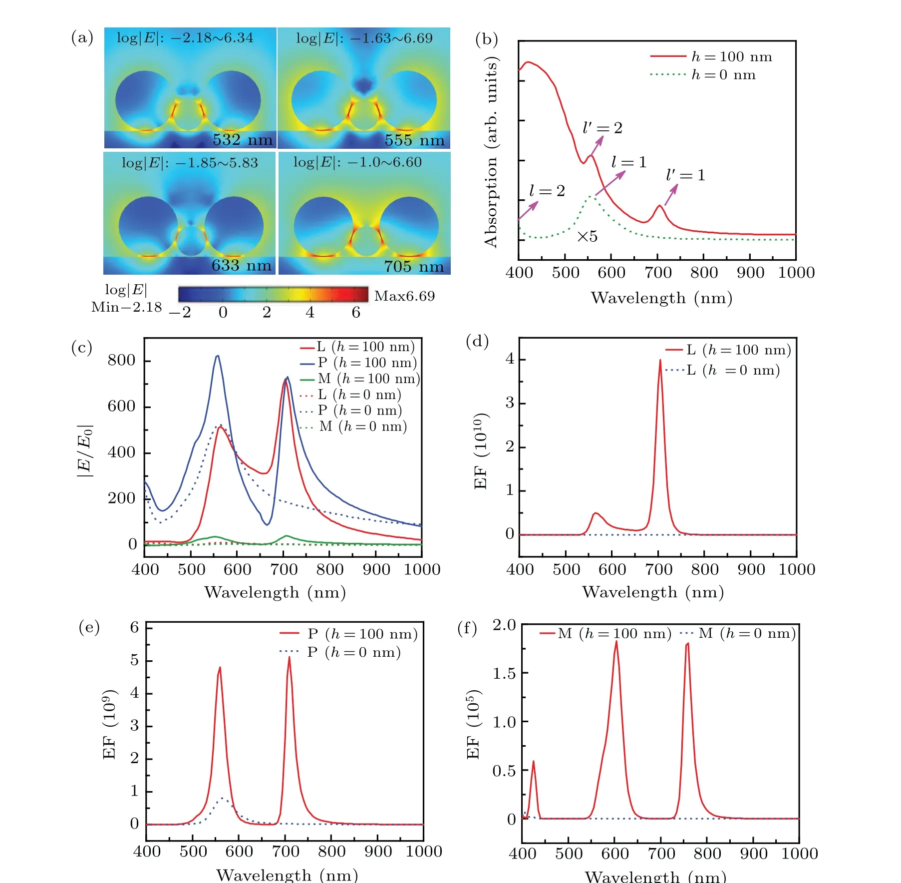
Fig.2. The focusing effect responsing to excitation wavelength in the 80-40-80 system. (a)Electric field distribution of Ag trimer-film system under the excitation wavelengths of 532 nm, 555 nm, 633 nm, and 705 nm, respectively. The diameter of sides’ nanoparticles is 80 nm and that of middle one is 40 nm in the system. (b)The absorption spectra of the trimer on Au film system(red solid line)and the trimer on glass substrate(green dot line,which is magnified 5 times for better contrast). The resonant modes for the trimer on Au film are labelled as l′=1 and l′=2,and for the trimer on glass substrate the peaks indicated by l=1 and l=2. (c)Electric field enhancement spectra in the gaps L,P,and M as indicated in Fig.1. The green,red,and blue solid lines represent the values of the gaps M,L,and P,respectively. The dot lines in different colors indicate the spectra in the corresponding gap in the case of Au film thickness h=0 nm. (d)-(f)The spectra of average enhancement factor in the gaps L,P,and M.The red dot line describes the EF spectra of the trimer on 100-nm thick Au film in different gaps. The blue dot line describes the EF spectra of the trimer on glass substrate(Au film thickness h=0 nm)in different gaps.
3.3. Nanoparticle size affecting on focusing effect
This light focusing is also affected by nanoparticle size.When the diameter of the middle NP changes, the electric field enhancement performance is investigated in the trimerfilm system. Figure 3(a)presents the absorption spectra of the trimer-film system with different diameters of the nanoparticles. In the trimer-film system,the diameters of the two-side NPs in the system is fixed to be 80 nm. The diameters of the middle NP would vary from 40 nm to 140 nm. For each of the above structures there are all two strong resonant plasmon modes. The two modes locate respectively in the longer wavelength region of 705 nm to 920 nm(labeled asl′=1)and in the shorter wavelength region of 705 nm to 920 nm (labeled asl′=2). Figures 3(b)-3(c)are the electric field enhancement spectra in the gaps L and P. The strong electromagnetic enhancement is shown at the corresponding peaks,especially at the peakl′=1. The same phenomenon for the enhancement in the gap M(see Fig.S3(a)in supporting information)is always weaker than that in the gaps L and P.In addition, when the particle diameters are 60 nm-140 nm,the EF in the gap L will reach 11 orders of magnitude at the peakl′=1 (see additional file, Figs. S3(b)-S3(d)). According to the hybridization theory of particles and films,[30]for such induced imaging charge coupling,the system is always a bonding mode,which leads to lower energy. If the coupling is stronger, the energy will be lower (red shift). It is obvious that both the plasmon modes have a redshift as increasing the diameter of the middle NP. The model′=1 shifts much greater and the model′=2 shifts smaller. We take the 80-80-80 system as an example to investigate the modes of the two resonant peaks with a hybridization point of view. The 80-80-80 trimer in air(neither on Au film nor on glass substrate)has two main resonant modes:l=1 at 636 nm andl=2 at 428 nm(see Fig.S1(b)in supporting information).The surface charge distribution in the NPs is corresponding to a large dipole mode. When the trimer couples with Au film the levelsl′=1 (796 nm) andl′=2(580 nm) appear which are attributed to the hybridization of levels 1 and 2 with the bonding and anti-bonding modes of the metal film. For model′=1, the trimer offers three bonding dipoles plasmon modes while the Au film offers one dipole.So this model′=1 contains four dipoles and can be considered as a pair of quadrupoles. The energy will decrease in the system. For the model′=2,the excitation polarization is almost vertical to the axis of the trimer, so the system behaves like each nanoparticle coupling with their induced dipoles in the Au film. The trimer and the Au film both offer three bonding dipoles plasmon modes,so model′=2 can be considered as the one containing three quadrupoles and be treated as a higher order plasmon mode with respect to model′=1. As a conclusion,model′=1 occurs at longer wavelength and model′=2 at shorter wavelength. For other trimer-film systems in which the diameters of the middle nanoparticles are different,the cases of hybridization are similar. But it is worthy of paying attention that the two hybridization bonding modes exhibit redshift as the diameter of the middle nanoparticle increases,which arises from the fact that the modesl=1 andl=2 in the trimer without film will redshift with the diameter increasing(see Fig.S4 in supporting information). The model′=2 as a higher order exhibits small redshift. However the model′=1 derives from coupling of the dipole mode with bonding mode,so the redshift is larger.
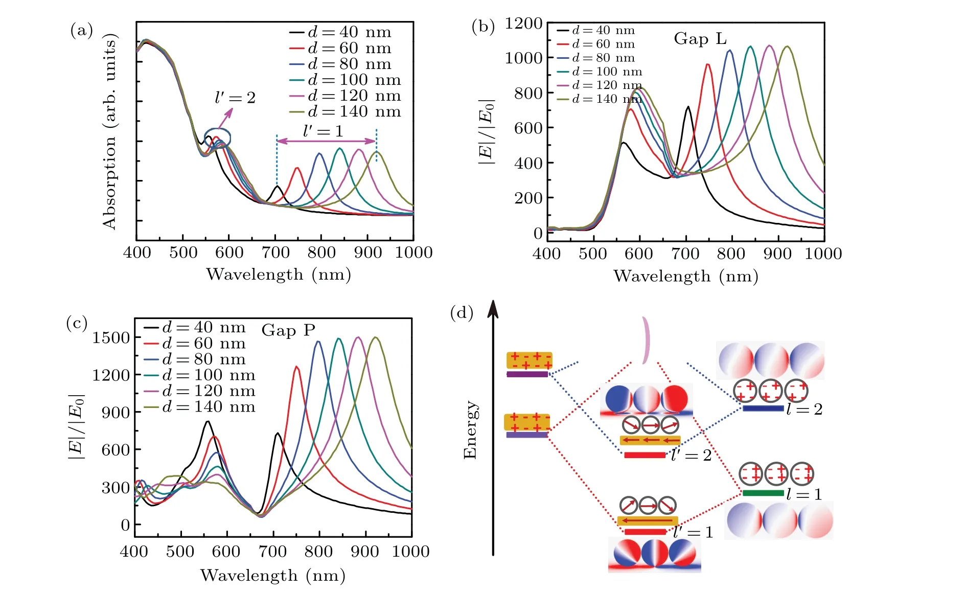
Fig.3. The light focusing dependence with nanoparticle size and hybrid analysis. (a)The absorption spectra of different trimer-film systems,in which the diameters of the sides’ particles are fixed to 80 nm and the middle particles diameter is varied from 40 nm to 140 nm, and the thickness of the Au film is 100 nm. (b)-(c)Simulated electric field enhancement in the gaps L and P in the trimer-film systems with different diameters of the middle nanoparticle. (d)Plasmonic hybridization of the 80-80-80 trimer-film system and the surface charge distributions corresponding to the plasmon modes l′=1,l′=2,l=1,and l=2.
4. Conclusions
In this work, the electric field redistribution and the energy focusing effect in linear trimer on metal film system with different excitation wavelengths and diameters of nanoparticles are investigated.The trimer-film system is designed in the present work,the ability of light energy focusing on the film is very obvious.The average enhancement factor can reach 9-10 orders of magnitude in the gaps L and P,which could yield a high plasmonic detection performance for SERS.At the same time, the SERS enhancement intensity at different gaps has huge difference in the trimer-film system in this work. The strongest enhancement spots would shift between gap L and gap P with the incident wavelength changing, which is good for selectively absorbing molecule at different positions under different wavelengths in SERS. We found the middle NP in the linear arranged trimer-film system has a very poor ability to confine light energy on the film no matter what the wavelength or diameter is,but which would impact on the position of the enhancement peak. The efficient excitation wavelength can be modulated in a wider range by changing the diameters of the middle NP. Our work on linear nanoparticle trimer on metal film has enhanced the research on surface plasmon of nanoparticle aggregation and is of great value in light energy focusing which could be applied to SERS,sensing,photocatalysis,solar cell,and other surface plasmon-related fields.
Acknowledgements
Project supported by the National Key Research and Development Program (Grant No. 2019YFC1906100), the National Natural Science Foundation of China (Grant Nos. 11974067 and 12074054), the Natural Science Foundation Project of CQ CSTC (cstc2019jcyj-msxmX0145,cstc2019jcyj-bshX0042, and cstc2019jcyj-msxmX0828), and the Sharing Fund of Chongqing University’s Large-scale Equipment.
杂志排行

Chinese Physics B的其它文章
- Superconductivity in octagraphene
- Soliton molecules and asymmetric solitons of the extended Lax equation via velocity resonance
- Theoretical study of(e,2e)triple differential cross sections of pyrimidine and tetrahydrofurfuryl alcohol molecules using multi-center distorted-wave method
- Protection of entanglement between two V-atoms in a multi-cavity coupling system
- Semi-quantum private comparison protocol of size relation with d-dimensional GHZ states
- Probing the magnetization switching with in-plane magnetic anisotropy through field-modified magnetoresistance measurement