Spin transport properties for B-doped zigzag silicene nanoribbons with different edge hydrogenations
2022-01-23JingFenZhao赵敬芬HuiWang王辉ZaiFaYang杨在发HuiGao高慧HongXiaBu歩红霞andXiaoJuanYuan袁晓娟
Jing-Fen Zhao(赵敬芬), Hui Wang(王辉), Zai-Fa Yang(杨在发), Hui Gao(高慧),Hong-Xia Bu(歩红霞), and Xiao-Juan Yuan(袁晓娟)
Keywords: silicene nanoribbons,spin filtering effect,negative differential resistance
1. Introduction
Silicene, as a hexagonal honeycomb monolayer nanomaterial, has been successfully synthesized on Ag(111),ZrB2(0001),and Ir(111)substrates.[1-3]Unlike graphene,silicene has a buckled structure rather than a planar one.[4]The altitude difference between two adjacent Si atoms is calculated to be about 0.5 ˚A (low-buckled geometry) due to mixed hybridization of sp2and sp3instead of the entire sp2hybridization in planar graphene.[5]In the face of low-buckled structure, silicene has not only the similar outstanding electronic characteristics to graphene but also some more superior features, for instance, a stronger spin-orbit coupling,[6]a better bandgap adjustability,[7]the quantum spin hall effect,[8]an easier valley polarization,[9]etc. Specifically, the successful synthesis of silicene nanoribbons (SiNRs) offers a new opportunity towards many potential applications, for example,field-effect transistors and spintronics devices.[10]In addition,silicene owns an distinct natural advantage over graphene,that is, its superior compatibility with today’s silicon-based semiconductors.[11]
Like graphene and graphene nanoribbons (GNRs), silicene and silicene nanoribbons(SiNRs)are also attracting increasing interest.[12-18]The silicene and SiNRs share a similar electronic structure to that of graphene and GNRs.[19-23]Therefore, two types of silicene nanoribbons can also be formed: armchair-edged silicene nanoribbons (ASiNRs) and zigzag-edged silicene nanoribbons (ZSiNRs). The two edge states of ZSiNRs are also anti-parallelly(AP)coupled,and the magnetic half-metal state can be achieved by breaking the inversion symmetry through applying a transverse electric field field. Moreover, the ZSiNRs are found to involve additional compelling properties, such as the electric-field-controlled gaps, symmetry-dependent transport properties, and highZTvalues of thermoelectric performance.[24-26]The most attractive signature of silicone and SiNRs is the potential gapless connection to the traditional silicone semiconductor based microelectronics and spintronics. To realize the magnetic modulation and spin polarized transport in ZSiNRs, extensive attention is paid to the edge modifications and substitutions in ZSiNRs.[27-33]If the silicon atoms on the edges are passivated in different methods,great changes occur in band structure,magnetic structure,edge states,and energy difference between the antiferromagnetic (AFM) and ferromagnetic (FM)states can be observed in the ZSiNRs.[27]Zhenget al.have presented a systematic study of the geometric, electronic and magnetic properties of N-or B-doped SiNRs,and their results showed that the substitution of N or B for Si is preferentially at the ribbon edge sites.[30]In this study,we theoretically design a set of boron (B)-doped ZSiNRs junctions as shown in Fig. 1 and concentrate on the influence of chemical doping combined with different edge hydrogenations. Our research shows that the electric current polarization in symmetric Bdoped ZSiNRs can reach 58%at a certain bias voltage. Additionally,the NDR behavior is achieved in asymmetric sp2-sp3edged ZSiNRs. However,the symmetric dihydrogenation exhibits spin degeneracy.These results lead to another method to control spin-polarized current and to design the silicene-based spintronic devices.
2. Theoretical models and calculation methods
The geometric structures of B-doped ZSiNRs with ribbon width that 5 silicon dimer lines cross from top and side view are shown in Fig.1. Generally,the bare edge of ZSiNRs is exceedingly reactive because of the hanging bonds of border Si atoms and undergoes rebuilding to reduce the total energy. Edge modification can enhance the property of ZSiNRs and thus enlarge ZSiNRs’ applications in the field of electronic devices.[34]In this study,H atoms are adopted to chemically decorate the edge state,and three different junctions are constructed,which are called H15ZSiNR-H1,H25ZSiNR-H1,and H25ZSiNR-H2, respectively. The H1and H2denote that the silicon atoms on the edges are terminated by one or two hydrogen atoms. Then=5 is the number of silicon dimer lines across the ribbon width. For the memorization purposes,these three junctions are separately denoted as M1, M2, and M3. The junctions can be divided into three blocks: the semiinfinite left electrode labeled by translucence pink shadow,the intermediate scattering section,and the semi-infinite right electrode labeled by translucence olivine shadow. Each electrode is denoted by two repeated unit cells along the transport direction, and the scattering section includes nine unit cells.Generally speaking,the magnetism of the two(left and right)electrodes can be adjusted to spin parallel (P) or antiparallel(AP) conditions via regulating the external magnetic field of electrodes.[35,36]Thus in this work we show a detailed research of the spin transport properties by boron-doped SiNR with different edge hydrogenations.
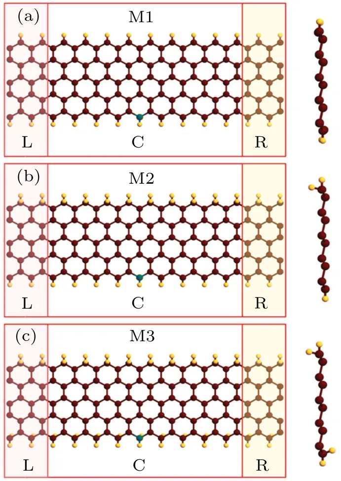
Fig.1. Structural models for 5-ZSiNR two-probe systems from top(left)and cross section view(right). Purple(yellow)circles denote Si(H)atoms, and green circles represent that Si atom is substituted by B atom.
The structural optimization and the spin transport properties are performed by theab initiocode package Atomistix ToolKit (ATK), which is on the basis of spin-dependent density functional theory (DFT) combined with nonequilibrium Green’s function (NEGF).[37-40]The mesh cutoff is set to be 110 Ry and thek-sampling is 1×1×100. The exchange and correlation potential adopts the Perdew-Zunger parametrization of the local spin density approximation (LSDA). A vacuum area of 10 ˚A is used for forbidding the interactions between periodic images. The structural optimization is implemented by using the quasi-Newton method till the absolute value of force acting on each atom is<0.02 eV/˚A. Under a certain bias (Vbias), the spin-related current through the junctions can be performed by the Landauer-B¨uttiker formula:[41]
wherehdenotes the Planck constant,eis the elementary charge,σrepresents the spin index which areσ=↑(spin-up)andσ=↓(spin-down).µL=EF+eV/2 andµR=EF-eV/2 are the electrochemical potentials respectively corresponding to the left and right electrodes. The chemical potential of left(right) electrode will shift down (up) byeV/2 when the positive bias voltage is applied to the left electrode. The energy range [µL,µR] devoting to the total integral current is named the bias window, andTσis the spin-dependent transmission,which can be calculated from
whereGRσandGAσrepresent the retarded and advanced Green function,ΓLσandΓRσdenote the spin-dependent coupling matrixes resulting from the coupling of the central scattering region to the left and right electrodes.
3. Calculation results and discussion
To further study, we calculate the spin-resolved currentvoltage(I-V)of M1-M3 in a bias range from-2.0 V to 2.0 V as given in Figs. 2(a)-2(c). We mainly consider the current quality under the P magnetism condition, that is to say, the two electrodes with identical spin orientation (the left electrode is spin polarized upward and the right one is also upward). As can be seen from Fig. 2(a), the tunneling current passes through the device is spin-polarized. This phenomenon is desired for spin filter or spin valve. The spin-down current (I↓) is greater than spin-up one (I↑) within a bias scope from-0.8 V to 0.8 V.We can see clearly that theI↓increases rapidly with the increase ofVbias,whereas theI↑maintains extremely small even on the verge of zero over a wide range of bias voltage. This result clearly indicates that the suggested junction under the P magnetism can display a spin filter effect in a low bias range. To analyze this phenomenon as shown in Fig. 3, the relevant spin filtering efficiency (SFE) is obtained from the equation SFE=[(I↓-I↑)/(I↓+I↑)]×100%.For zero bias, the SFE is calculated through this formula:SFE=[(T↓(EF)-T↑(EF)]/[(T↓(EF)+T↑(EF)]×100%, whereT↑(EF)andT↓(EF)denote the transmission coefficients of different spin states at the Fermi level(EF),respectively. We can find that the SFE at zero bias voltage can reach 32%and a high spin filter status can be maintained in the scope of positive and negative bias which is on the verge of 40%. Particularly, the SFE can be up to 58.3%atVbias=-0.5 V.But the SFE shows a downward trend when the bias is beyond this region. Yet for the M3 system as illustrated in Fig. 2(c), the currents (I↓andI↑) are both basically prohibited in low bias range from-1.0 V to 1.0 V.While it is allowed to pass through in the high bias range for both up current and down current. These results show that the spin-polarization at M3 is suppressed and therefore exhibits nonmagnetic phenomenon. In the case of M2(in Fig.2(b)),the current in spin-up state grows rapidly in the low bias region and then it falls down with the bias increasing.This phenomenon indicates the appearance of negative differential resistance(NDR)effect which has very important applications in the field of electronic technology.
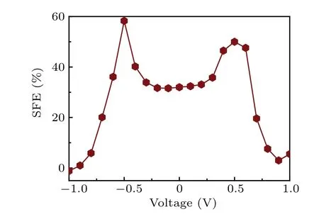
Fig. 2. Spin-dependent current for models M1-M3 under P spin configuration at various biases,with I↑referring to blue block and I↓representing red block.
To explain the spin filter phenomenon,the band structure and the transmission spectra for junction M1 atVbias=0.2 V are calculated and presented in Fig.4,which is a most intuitive understanding of electronic structures and quantum transport behaviors for an electronic device. As can be seen from the band structure diagram of M1 (Fig. 4), the bands of spin-up state and spin-down state atEFare split. Further study shows that when a positive bias of 0.2 V is applied,the chemical potentials move downward along the left electrode and upward along the right electrode, within the bias window, theπ*(π)subband of left electrode overlaps with theπ*(π)subband of right electrode for spin-up(spin-down)state. From previously published study, it is well recognized that the transport characteristics of ZGNRs are strongly dependent on symmetry and the presence of a mirror planeσis of great concern.[42]TheI-Vproperties of ZGNRs are quite different between the cases with and without theσmirror plane.That is to say,if the width is even,the ribbon exists a symmetrical midplaneσ,whereas if width contains the odd number of silicon dimer lines, such a midplane is absent. Unlike the ZGNRs,the ZSiNRs have no definite parity relative to theσplane due to the wrinkled structure,but hasC2symmetry relative to a twofold axis when the width contains the even number of silicon dimer lines. Thus the pristine ZSiNR also shows a symmetry-dependent transport property although it has a buckled structure, where oddand even-width zigzag ribbons are found to have completely differentI-Vcharacteristics despite the similarity of their band structures. For example, bipolar spin-filter behavior is observed in even-width devices, while in the odd ones a linearI-Vcurve characteristic limits their applications in spintronic devices.[25]In this case, since the width is odd (5-ZSiNRs)thus there is noC2symmetry relative to the center axis. Thus itsπband andπ*band have no definite parity under theC2operation. Without the limitation of parity, the electronsno matter whether their spins are up or down should both traverse from the left electrode to the right electrode, finally generate a strong transmission coefficients. Paradoxically, we can see from the middle row of Fig.4 that there exists a wide transmission coefficient for spin- down electrons in the bias window.However, for the spin-up ones, as only a small transmission peak exists above theEFin the bias window,the transmission coefficient is relatively small. Consequently, the large spindown current appears.

Fig. 4. Band structures and transmission spectra for junction M1 at Vbias =0.2 V, with area between two black dotted lines denoting bias window, and blue line and red lines representing spin-up and spin-down transmission spectra,respectively.
In order to better analyze the above spin-resolved transport property, we show the spatial-resolved local density of states(LDOS)atEFand the transmission eigenstates of junction M1 under 0.2 V (Figs. 5 and 6). To our surprise, the magnetic properties of the device can be modulated by using B dopant, especially for up-spin electron state. As can be seen from Fig.5,the LDOS of spin-down electrons is well delocalized. This means that the spin-down electrons can pass through the intermediate scattering section and reach the right electrode,while the spin-up electrons are mainly distributed at the edges of the nanoribbon and are heavily localized. This phenomenon will lead the transmission channel to forbidden,corresponding to the small transmission coefficent in the middle row of Fig.4. To further study, the spin filtering effect is also reflected in the spin-dependent transmission eigenstates underEFas shown in Figs.6(a)-6(d). The transmission eigenstates of bothπandπ*for the spin-up electrons are highly localized. This results in a blockade of electronic transmission.Conversely, the eigenstate ofπfor the spin-down (Fig. 6(c))electron is continuously distributed along the nanoribbon. It is obviously seen that the LDOS and the transmission eigenstates of spin-down electrons are more delocalized than the spin-up ones. This indicates that the spin-down electrons dominate over the spin-up electrons, resulting in the perfect spin filtering effect.
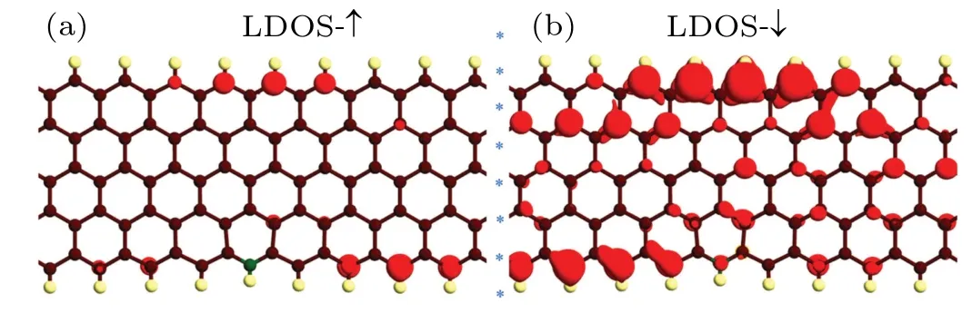
Fig.5. Spin-resolved LDOS at EF of junction M1 at Vbias =0.2 V,and isovalue 0.02 a.u.
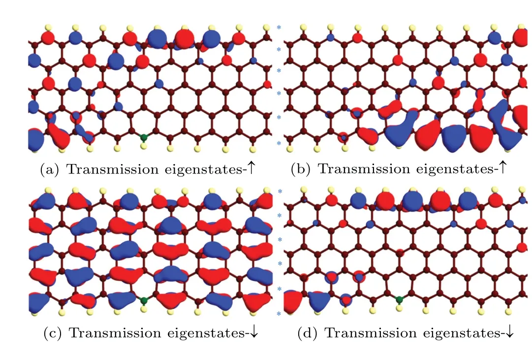
Fig. 6. Spin-dependent transmission eigenstates at EF of M1 under Vbias =0.2 V and isovalue 0.05 a.u.
For further exploration, since the edge effect is a significant influence factor for nanoribbons, the effects of different edge hydrogenations on the transport properties are also considered by M2 and M3, and the conductivity of edgedoped junction M3 and the corresponding LDOS are discussed. When the edge silicon atom is hydrogenated with two H atoms,the band structure(Vbias=1.5 V)is obviously different from the counterpart of the M1 system as shown in Fig.7.The results show that the spin-up and spin-down bands are completely degenerate and theπandπ*bands nearEFappear slightly dispersive in contrast to the scenario in M1 case. And a 0.51-eV band gap is opened, which shows up a semiconducting character. From theI-Vcurve (Fig. 2(c)) it follows that the currents(I↓andI↑)are almost zero in the low bias region, however they are allowed to pass through the high bias range. Like the case of M1, when the positive bias of 1.5 V is applied, the chemical potentials move downward along the left electrode and upward along the right electrode,and in the bias window, theπandπ*bands for both spin-up electrons and spin-down electrons of the two electrodes overlap. Similarly, due to then=5 is also odd, thus itsπandπ*bands have no definite parity under theC2operation. Without the limitation of parity,the electrons no matter whether their spins are up or down should both traverse from the left electrode to the right one, generating strong transmission coefficients.As presented in the transmission spectrum (Fig. 7), there exist indeed more transmission coefficients entering into the bias window. For the subsequent analysis,we present in Fig.8 the spin-correlated LDOS of device M3 atEFunder 1.5 V.We can see that the LDOS of both spin-up and spin-down electrons are delocalized. This indicates that the electrons can pass through the intermidiate scattering region and reach the right electrode.This is consistent with the calculated transmission spectrum as shown in Fig.7.
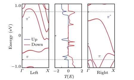
Fig. 7. Band structures and transmission spectra for junction M3 at Vbias =1.5 V,with region between two black dotted lines denoting bias window,and blue line and red line representing spin-up and spin-down transmission spectra,respectively.
Finally,we focus on the NDR phenomenon appearing in the spin-up state of device M2 as shown in Fig.9. On the basis of Landauer-B¨uttiker equation(1),the spin-dependent current across the intermediate scattering section is determined by the transmission coefficient in the bias window. Thus the current and voltage transport characteristics can be analyzed through the transmission spectra.[43,44]Figure 9 shows the spin-up transmission spectra under three different biases. AtVbias=0.7 V(Fig.9(a)),it is found that the transmission coefficients in the bias window are relatively large. When the bias increases up to 1.0 V(Fig.9(b)),the transmission peak under the integral area becomes small. This means that the current decreases with the bias voltage increasing. As the bias reaches to 1.3 V(Fig.9(c)), more transmission coefficients enter into the bias window,and thus causing the current to increase. As a consequence,an NDR behavior appears in the spin-up state.

Fig.8. Spin-resolved LDOS at EF of junction M3 at Vbias =1.5 V and isovalue 0.02 a.u.
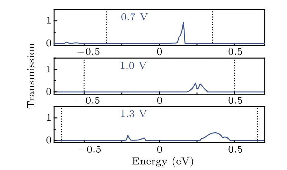
Fig.9. Transmission spectra for spin-up channels at various voltages of junction M2,with blue line denoting transmission spectrum and black dotted lines representing integral window.
4. Conclusions
In summary, we have investigated the spin-correlated transport properties of different edge hydrogenated zigzag silicene nanoribbons with edge-doped boron atoms by regulating the electrode magnetism in P configuration. The spin filter effect (with nearly 60% SFE) and NDR behavior can be obtained. We also find that the spin-polarization at device M3 is compressed. This is attributed mainly to the perturbation of B-doping localized at the edge. The physical mechanisms of these interesting properties are analyzed by the spin-resolved transmission spectra, the transmission eigenstates, the band structures, and the symmetry of ZSiNR electrodes. Based on the multiple spin-dependent transport properties, there are some potential applications in spintronics.
Acknowledgements
Project supported by the National Natural Science Foundations of China (Grant No. 11574118) and the Natural Science Foundation of Shandong Province, China (Grant No.ZR2019PEM006).
猜你喜欢
杂志排行

Chinese Physics B的其它文章
- Superconductivity in octagraphene
- Soliton molecules and asymmetric solitons of the extended Lax equation via velocity resonance
- Theoretical study of(e,2e)triple differential cross sections of pyrimidine and tetrahydrofurfuryl alcohol molecules using multi-center distorted-wave method
- Protection of entanglement between two V-atoms in a multi-cavity coupling system
- Semi-quantum private comparison protocol of size relation with d-dimensional GHZ states
- Probing the magnetization switching with in-plane magnetic anisotropy through field-modified magnetoresistance measurement