Dependence of short channel length on negative/positive bias temperature instability(NBTI/PBTI)for 3D FinFET devices
2022-01-23RenRenXu徐忍忍QingZhuZhang张青竹LongDaZhou周龙达HongYang杨红TianYangGai盖天洋HuaXiangYin殷华湘andWenWuWang王文武
Ren-Ren Xu(徐忍忍) Qing-Zhu Zhang(张青竹) Long-Da Zhou(周龙达) Hong Yang(杨红)Tian-Yang Gai(盖天洋) Hua-Xiang Yin(殷华湘) and Wen-Wu Wang(王文武)
1Integrated Circuit Advanced Process Center(ICAC),Institute of Microelectronics,Chinese Academy of Sciences,Beijing 100029,China
2Key Laboratory of Microelectronics Devices&Integrated Technology,Institute of Microelectronics,Chinese Academy of Sciences,Beijing 100029,China
3University of Chinese Academy of Sciences,Beijing 100049,China
Keywords: bias temperature instability(BTI),channel length,stress,FinFET
1. Introduction
The introduction of high-k/metal-gate (HKMG) technology is greatly helpful for the improvement of the performance in the scaled metal-oxide-semiconductor field-effect transistor(MOSFET).However, it takes more serious challenges to the device’s reliability[1-3]due to the scaling of channel geometry and the structure evolving of basic transistors. Among these reliability issues, both negative bias temperature instability(NBTI) and positive counterpart (PBTI) have become one of the most critical reliability challenges.[1,4,5]In the BTI study,the investigation and understanding of the channel length scaling are paid more attention.[6,7]Regarding the gate length dependence of the device, the strong gate length dependence of hot carrier injections(HCI)[8,9]and light-emitting diodes have been systematically reported.[10]However, the previous research on BTI shows weak channel length dependence of BTI in planar or SOI transistors.[11,12]Recently, one simple relationship between the channel length and the BTI on 3D Fin-FETs is demonstrated, but without any physical explanation presented.[13]Usually,the physical mechanism of BTI degradation is process-related,such as interface quality[14]or oxide defects,[15-17]diffusion of fluorine[15]and nitrogen.[3,18,19]It changes the device parameters such as threshold voltage,channel mobility,[20-22]trans-conductivity,and threshold slope and generally reduces the driving current of the field-effect transistor. Some studies attribute the correlations between BTI and the channel length to the electric field[11,16]and mechanical stress.[14,23,24]However, by now, there is no systematic study on channel length dependence of BTI for advanced Fin-FET devices. Therefore, in this work, the BTI characteristics of n-FinFET and p-FinFET with different short channel lengths(ranging from 30 nm to 100 nm)are extensively investigated. The experimental results demonstrate that both NBTI and PBTI of advanced FinFET devices are alleviated with a shorter channel length.A comprehensive physical explanation to the dependency based on traditional BTI mechanism and 3D channel stress simulation with Sentaurus tool is also presented for better understanding the critical characteristics in advanced FinFET process technologies.
2. Device and experiment
In this work,3D n-FinFET and p-FinFET devices with a high-k/metal gate process were fabricated on an 8-inch p-type Si bulk substrate with a crystal of orientation〈100〉and a resistivity of 8-12 Ω·cm. The fabrication process of the bulk silicon FinFET is shown in Fig. 1(a). Firstly, the 3D Si fin channel structure was constructed by the self-aligned spacer image transfer(SIT)method in the experiment. Then,the adjacent fins were isolated by deposited high aspect ratio process(HARP) shallow trench insulation (STI) oxides following by a chemical mechanical polishing (CMP) process and STI recess process. The punch-through stop (PTS) doping process was used to isolate the bottom Si substrate.[25]In the following steps,the dummy gate,spacer,source/drain(S/D)doping,and activation annealing were carried out in sequences.[25]The dummy gate was removed after the first inter-layer-dielectric(ILD0) deposition and planarization and then, a multi-layer HKMG process is performed. The gate films surround the silicon fin channel on three sides to form a multi-gate structure. During the process, the layers of TiAlC/TiN for NMOS and the layers of TiN/TaN/TiN for PMOS were deposited all by atomic layer deposition (ALD) methods. Finally, the S/D metal-contact and the metallization process were completed in next steps. The final structure of 3D bulk silicon FinFET is shown in Fig. 1, and the TEM images cross the channel directions of the n-FinFET and the p-FinFET are shown in Figs.1(b)and 1(c),respectively.
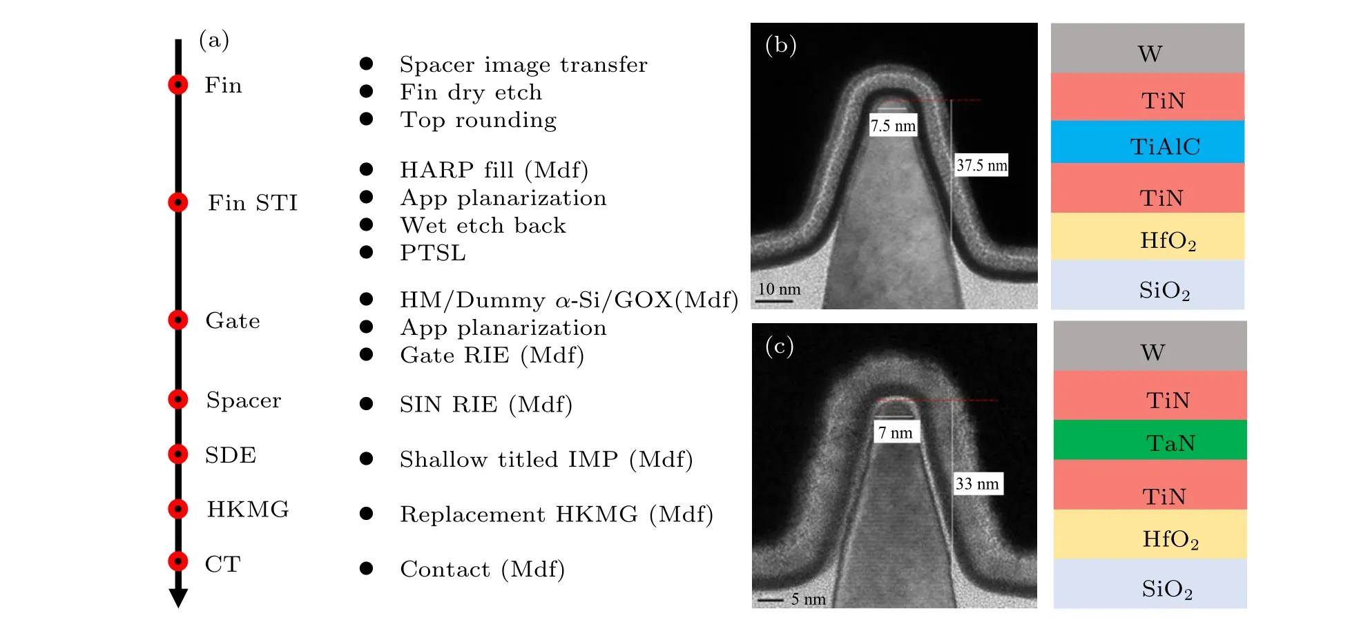
Fig.1. (a)Process flow of 3D bulk silicon FinFET.Cross-sectional TEM image and schematic diagram of the gate structure of(b)n-FinFET and(c)p-FinFET.
The NBTI of p-FinFETs and PBTI of n-FinFETs were measured at 125°C by using the conventional measure-stressmeasure (MSM) method.[26]Here, the samples were FinFET with 2 fins,and the designed channel lengths of devices were ranged from 30 nm to 100 nm. The threshold voltage(VT)was extracted by the constant current method with a targetIdlinof 200 nA×W/L,[26]whereWandLare channel width and channel length,respectively.
3. Results and discussion
3.1. Basic electrical characteristics
Figure 2 shows the typical electrical characteristics of n-FinFET and p-FinFET with short channel lengths(30 nm and 100 nm). TheId-Vgcurve shows good electrical characteristics, such as initialVT, subthreshold swing (SS), and large ratios ofIonandIoff(~106).
3.2. NBTI and PBTI characteristics of FinFETs
Figures 3 and 4 show theId-Vgcurves of p-FinFET and n-FinFET under-1/+1 V overdrive voltage (Vov) stress at 125°C with different channel lengths, such as (a) 30 nm,(b) 60 nm and (c) 100 nm, respectively. In Fig. 3, while the stress time increases from 1 s to 1000 s,theId-Vgcurve shifts to the left-direction. As shown in our previous work, both the positive interface trap and oxide trap are the sources of degradation due to NBTI in p-FinFET with a short channel length.[27]Similar to that in Fig. 3, theId-Vgcurves shifted to the right-direction with stress time increasing are shown in Fig. 4, and the negative oxide trap degradation almost dominates the source of the degradation for PBTI.[28,29]So,a negative oxide trap is critical for the analysis of the dependency of PBTI in n-FinFET.[3,30]
All extractedVTBTI kinetics of p-FinFETs and n-FinFETs with different channel lengths(30 nm,40 nm,60 nm,and 100 nm) under-1/+1 V overdrive voltage stress and 125°C are shown in Fig.5. It obviously demonstrates that the shorter the channel length, the better BTI degradation, which is totally similar to the previous report.[18]Here,the extracted data is the arithmetic average degradation of three samples for each BTI stress.
In order to make a relationship betweenVTshift and channel length,theVTshifts of p-FinFET and n-FinFET at 1000 s BTI stress are shown in Fig. 6. The results show that theVTshift of p-FinFET at 1000 s NBTI stress is obviously dependent on channel length, and the slope is almost 0.95 mV/nm.However, the dependence ofVTshift at 1000 s PBTI stress is less serious than those of NBTI,especially for that of 40 nm,60 nm,and 100 nm channel length.As we know,the trap in the oxide of p-FinFET is much greater than that of n-FinFET.[31]
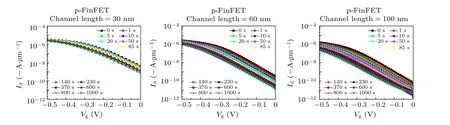
Fig.3. The Id-Vg curves of p-FinFET with different channel lengths of(a)30 nm,(b)60 nm,and(c)100 nm under-1 V overdrive NBTI stress at 125 °C.
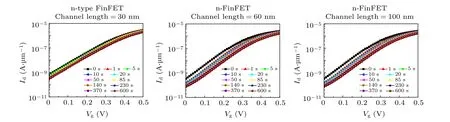
Fig.4. The Id-Vg curves of n-FinFET with different channel lengths of(a)30 nm,(b)60 nm,and(c)100 nm under 1 V overdrive PBTI stress at 125 °C.
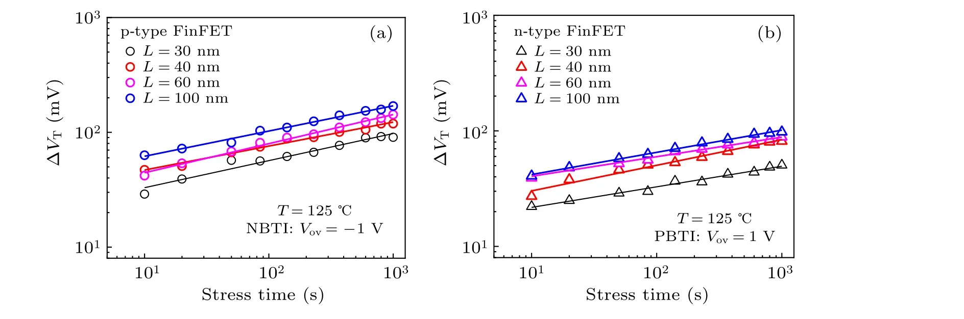
Fig.5. Extracted BTI kinetics of(a)p-FinFET,(b)n-FinFET with different short channel lengths under-1/+1 V overdrive voltage BTI at 125 °C.
When the gate voltage remains fixed and the gate length gradually decreases,the current and the amount of charge will increase. That is, the amount of charge trapped by the trap in p-FinFET is much more than that in n-FinFET, so the NBTI of the p-FinFET is much more serious than the PBTI caused by n-FinFET. Therefore, the possible reason why the channel length dependence on NBTI is more serious than that on PBTI is the more serious corner trap effect in NBTI than that in PBTI.

Fig.6.Relationships between Vth shift and channel length for p-FinFET and n-FinFET at 1000 s NBTI/PBTI stress.
3.3. Physical mechanism analysis
3.3.1. Physical mechanism analysis of channel length dependence in NBTI
As mentioned in Subsection 3.2,there are both effects of positive interface trap degradation and hole trapping in oxide on NBTI of p-FinFET with short channel lengths. At first,we discuss the influence of hole trapping in oxide on the dependency. Usually, fluorine can passivate oxygen vacancies with positive charges,[9]and the bonds formed by F and Si are much stronger than those with O.[10,11]Therefore,F-Si bonds are not easily dissipated during high-temperature processing and thus exert a certain influence on the NBTI effect of p-FinFET.In our previous work,[12]the fluorine diffusion from the metal gate(ALD W)may passivate the oxygen vacancies and alleviate the hole trapping in the HfO2high-klayer. As a result, a physical mechanism is proposed in Fig. 7. There is more fluorine diffusion in the gate corner, and thus there is less hole trapping in the oxide of p-FinFET with a shorter channel length (30 nm), which induces an NBTI degradation as channel length is reduced.Therefore,the channel length dependence of NBTI is partly due to the corner effect of fluorine passivation from the ALD W process.
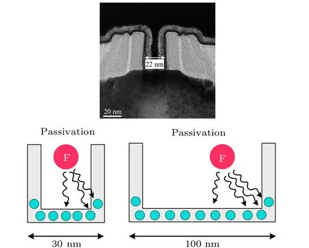
Fig.7.The passivation effect of fluorine diffusion in the corner of oxide is more serious in the p-FinFET device with shorter channel length(the circles are hole traps in oxide).
On the other hand, we discuss the influence of the interface trap degradation in the NBTI of p-FinFET, in which the NBTI on channel length dependency is often attributed to the effect of mechanical stress.[23,24]In this paper, the 3D stress TCAD simulation of p-FinFET with different channel lengths is performed and the results are shown in Fig.8. Figures 8(a)and 8(b)are 1-D and 3-D stress profiles along the ZZ channel direction of p-FinFET,respectively. The results show that the channel stress at a channel length of 30 nm is almost twice of that of a channel length of 100 nm. As we know, due to the shrinking of the channel length of the FinFET, the strain caused by mechanical stress becomes larger. The strain affects the structure of the energy band,increasing the effective mass,[23,24]which will decrease the mobility of carriers and the drive current of the device, and ultimately lead to a decrease in theVTof the device. Therefore,the smaller the channel length,the larger the mechanical stress,the smaller theVT,and the weaker NBTI degradation.
Hence, both the extra fluorine passivation in the corner of bulk oxide and the greater mechanical channel stress in the shorter channel induce less NBTI degradation of p-FinFET.
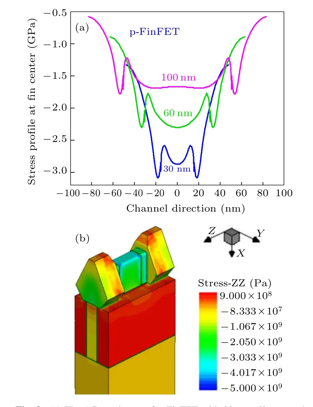
Fig. 8. (a) The 1-D strain cut of p-FinFET with 30 nm, 60 nm, and 100 nm channel length. Along with the channel direction, (b) strain TCAD simulation of 3D p-FinFET with 30 nm.
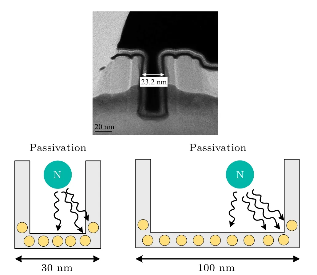
Fig. 9. The passivation effect of nitrogen diffusion from ALD TiN in the corner of oxide is more serious in the n-FinFET device with short channel length(the circles are electron traps in oxide).
3.3.2. Physical mechanism analysis of channel length dependence in PBTI
As mentioned in Subsection 3.2,the electron trapping in bulk oxide dominates the PBTI degradation of n-FinFET.Similar to the fluorine diffusion in NBTI for p-FinFET,the nitrogen diffusion from ALD TiN in metal gate due to precursor is attributed to the channel length dependence on PBTI. It is well known that nitrogen is a good passivation atom to negative oxygen vacancy in HfO2,[3,18,19,32]so for transistors with shorter channel lengths,more percentage of nitrogen passivation occurrs in the corner of bulk oxide and therefore, less PBTI degradation achieved. However, nitrogen is a composition element, so the dependence is not serious like that in NBTI.
4. Conclusion
The NBTI of p-FinFET and PBTI of n-FinFET with different short channel lengths are systemically investigated. The results show that with channel length shrinking from 100 nm to 30 nm, the device with a shorter gate length shows better BTI reliability. Moreover, the channel length dependence of NBTI is more serious than that of PBTI of n-FinFET under the same overdrive gate bias and stress time. Both the corner effect of fluorine diffusion from ALD W and the strong channel stress is the source of channel length dependence on NBTI of p-FinFET.On the other hand, the corner effect of nitrogen diffusion from ALD TiN is the main reason for the dependence of channel length on PBTI of n-FinFET.The proposed physical mechanism is well matching the experimental results and helps to guide the process optimizations in advanced FinFET fabrication technology with a short channel length for better reliability.
Acknowledgments
Project supported in part by the Science and Technology Program of Beijing Municipal Science and Technology Commission,China(Grant No.Z201100004220001),the National Major Project of Science and Technology of China (Grant No.2017ZX02315001),and the Opening Project of Key Laboratory of Microelectronic Devices&Integrated Technology,Institute of Microelectronics, Chinese Academy of Sciences(Grant Nos. Y9YS05X002 and E0YS01X001).
猜你喜欢
杂志排行

Chinese Physics B的其它文章
- Superconductivity in octagraphene
- Soliton molecules and asymmetric solitons of the extended Lax equation via velocity resonance
- Theoretical study of(e,2e)triple differential cross sections of pyrimidine and tetrahydrofurfuryl alcohol molecules using multi-center distorted-wave method
- Protection of entanglement between two V-atoms in a multi-cavity coupling system
- Semi-quantum private comparison protocol of size relation with d-dimensional GHZ states
- Probing the magnetization switching with in-plane magnetic anisotropy through field-modified magnetoresistance measurement